AMAZON multi-meters discounts AMAZON oscilloscope discounts
Passive filters are built solely from passive components such as resistors, capacitors and inductors.
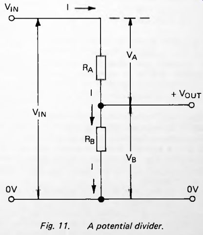
Fig. 11. A potential divider.
Before explaining how passive filters work, let us look at a very commonly used sub-circuit, the potential divider (p.d.) (Fig. 11). A current I flows from the positive input terminal, through resistor A, then through resistor B and to the negative line. We are assuming for the moment that there is no other circuit connected to the output terminals, so that all the current flowing through A also flows through B.
Since the current is the same throughout, the p.d. across each resistor is proportional to their resistances, as is the p.d. V_in across the two resistors in series. The output p.d. of this sub-circuit (or network, as it is more often called) is V_B which we will from now on refer to as V_out. Since p.d.s are proportional to resistances, we can write:

--------
…which gives the result:
This equation holds true provided that no current or only a small current is being drawn from the output side. If a larger current is drawn, this has the same effect as putting another resistor in parallel with R%. This reduces the effective resistance of the lower section of the network and thus reduces Pout The potential divider has been discussed as if Vin is a steady (= d.c.) potential). However, the relationship between current, resistance and voltage is instantaneous so that Vin could equally well be an alternating signal. In this event Pout is an alternating signal of the same form as the input signal but with its amplitude reduced in the ratio R_B/ (Ra + Rb)
In Figure 12(a) we have substituted a capacitor for R_B. The reactance of the capacitor takes the place of R B of Figure 11, but since reactance has some of the properties of resistance, we still have a potential divider network. But there is one important difference. The reactance of the capacitor depends upon the frequency of the input signal Vin, and so does the output of the network.
Fig. 12. Two ways of drawing a low-pass filter.
The p.d.s in this network can be equated to the p.d.s of Figure 7. V_IN corresponds to V_T and V_out corresponds to V_c. Figures 8 to 10 explain how this type of potential divider behaves with signals of different frequencies. If the frequency of the signal and the value of the capacitor are such that Xc = R, we have the situation shown in Figure 8. In Figure 8, the amplitude of V_T is approximately 1.4 times Vc so, in Figure 12(a) the amplitude of V_out (i.e. V_c) is approximately 1/1.4 times that of V_in (i.e. V_T). Converting this to decimals we find that V_out is approximately 0.7 times V_in. In addition, it lags behind V_in by 45°. We say that phi = -45°. This is a situation that we shall return to again shortly.
Figure 9 shows the signals when the frequency is lower than that in Figure 8. Here V_out (= Vc) is about 0.84 times V_in (= Ft). The exact amount is not important in this discussion--the point is that FOUT is relatively larger at low frequency, though still less than Fm. The phase angle between V_in and V_out is now phi = -30°, a smaller lag.
In Figure 10, in which frequency is 5 times that in Figure 8, V_out is only about 0.2 times V_IN. There has been a marked reduction in amplitude. The phase angle Phi has increased to about -80°.
Summing up, the network of Figure 12(a) acts as a potential divider with a frequency dependent 'resistor'. Low-frequency signals pass through it with little reduction in amplitude; high-frequency signals are very much reduced.
This network is therefore a low-pass passive filter. Figure 12(b) shows the same network with the resistor drawn at a different angle, which is how we usually draw such a filter.
Filter Characteristics
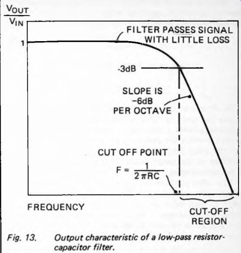
Figure 13
Figure 13 sums up how the ratio of V_out/V_in varies with frequency. At low frequency the reactance of the capacitor is very high, so that virtually the whole signal appears at the output. At slightly higher frequency the reactance increases to the extent that the output shows a significant drop. We reach the point illustrated in Figure 8 at which the resistance and the reactance are equal in value and V_out 0.7 times V_in. This is known as the cut-off point of the filter. There is a certain amount of reduction of signal strength at frequencies below this point, but this point is usually taken as the standard point when describing the characteristics of a filter. As shown on page 12, the frequency at the cut-off point is / = 1/ 2 pi RC.
Above the cut-off point the output begins to drop more sharply. It assumes a steady downward gradient. At even higher frequencies the reactance is so high that virtually nothing of the signal remains.
To understand this graph fully we have to know what is meant by the term decibel, symbol dB. The decibel is a way of expressing the ratio between two quantities. Here we use it to express the ratio of V_out to V_in. The ratio is calculated like this:
n--20 x logic (V_out/V_in)
We use ' n ' as the subject of this equation to indicate that since we begin the calculation with a ratio, the result is a pure number. Decibels are not quantities such as volts, amps and ohms--they represent a ratio calculated in a particular way.
In Figure 8, the ratio V_out/V_in is 0.7.
Expressed in decibels, this becomes:
n = 20 x log100.7 = 20 x -0.1549 = -3dB .
The cut-off point is sometimes referred to as the 'minus 3 decibel' point.
The steady downward fall in response above the cut-off point can also be described in terms of decibels. In Figure 13 the slope is marked as 6dB per octave'. The equation on page 21, in reverse, specifies what a fall of -6dB means. If the ratio between input and output is a, then:
-6 = 20 log10a
log10a = -20/6 = -0.3
a = anti-log 10 -0.3 = 0.5
In other words, the signal amplitude is halved. This halving occurs for every increase in frequency of one octave. An octave represents a doubling of frequency just as on a piano keyboard where the frequency of the musical note A is 440Hz and the frequency of A', an octave above it, is 880Hz. A doubling of frequency results in a halving of the amplitude of the filter output.
The other characteristic of a filter that changes with frequency is the phase angle. We have already shown that this is -45° at what we now refer to as the cut-off point or -3dB point. The phase angle is less at lower frequencies and increases to a maximum of -90° at the highest frequency, but always V_out lags behind.
High-pass Filter
If the resistor and capacitor of Figure 12(a) are exchanged, we obtain a potential-divider network (Fig. 14) in which the output signal appears across the resistor. In terms of Figure 8, V_in is equivalent to V_T (the same as in the low-pass filter) but V_out now equivalent to V_R. As might be expected, the action of this network is the opposite of the low-pass filter. At the frequency when the R and Xc are equal, the V_out is 0.7 times V_in (remember that in Figure 8, V_R = V_C). In other words, this is the -3dB cut-off point. It occurs at the same frequency for both low-pass and high-pass filters.
Figure 15 shows that above the cut-off point the output increases a little until there is virtually no loss. The low-frequency section of the curve rises at +6dB per octave.
Two ways of drawing a high-pass filter. Fig. 14.
The effect of a high-pass filter on phase angle is the opposite to that of a low-pass filter. In such a filter the output is V_R. At the cut-off point, V_out leads V_in by +45° as before.
At lower frequencies the lead increases to a maximum of +90°. At higher frequencies it is less than +45°.
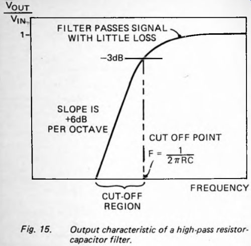
Fig. 15.
Orders
The two filters described above each consist of a single stage. We refer to these as first-order filters. Sometimes we wish to build a filter with a sharper cut-off, to obtain a characteristic curve with a slope greater than -6dB or +6dB per octave. One way of doing this is to use the output of one filter as the input of a second filter. This produces a two-stage filter, usually known as a second-order filter. Figures 16 and 17 respectively show second-order low-pass and high-pass filters. If both stages have the same cut-off points, their response characteristics are identical. In a first-order low-pass filter, the slope of the curve is -6dB per octave in the cut-off region. A second low-pass filter placed after this increases the slope of the curve by a further -6dB, giving a total reduction of -12dB per octave. This corresponds to reducing the input amplitude by a quarter per octave.
Adding a second stage to a filter also increases the phase angle. For example with two identical stages, each with 0 = -50°, the second-order filter has a total phase lag of 100°. Since the maximum lag of a single stage is almost 90°, the maximum lag of a second-order filter is 180°. In this case the input and output signals are of completely opposite phase.
This has an important bearing on filters used in certain types of oscillator circuits.

Fig. 16. A second-order low-pass filter.
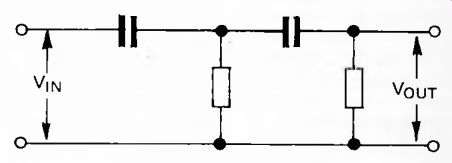
Fig. 17. A second-order high-pass filter.
Filters need not end at the second order. It is permissible to add even more stages, with a corresponding increase in the sharpness of cut-off. However when we add stages to a filter, even just adding the second stage of a second-order filter, we have to take into account the effect each succeeding stage has on the operation of the previous stages. As mentioned on page 18, the equations describing the action of a potential divider rely on there being no loss of current at the output.
Although loss of current can be minimized, it can not be prevented altogether. For this reason the cascading of stages does not necessarily produce a filter that behaves exactly as the 'sum' of its parts. Although cascading many stages may give a very steep slope to the curve in the cut-off region it has little effect in sharpening the 'knee' of the curve around the cut-off point. If requirements are relatively uncritical a second order filter constructed solely of resistors and capacitors may be acceptable. For filters of higher order a much better response is obtained by using inductors as well. As explained on page 14 these lead to other problems and the best solution is to turn to active filters, employing operational amplifiers. Filters of this type are described in the next few sections.
Another View of Filters As long as the input voltage to a low-pass filter (Fig. 12) is greater than the voltage already present across the capacitor, a current flows through the resistor, gradually increasing V_out (Fig. 18). Given that V_in is significantly greater than V_out, the rate of increase of V_OUT is approximately steady.
In this way V_out depends upon F0 the value it had to begin with, and how long V_in has held its present value. The circuit is performing the mathematical function of integration. The greater the value of V_IN and the longer the time, the greater the value of V_OUT. Similar reasoning applies if V_IN is varying.
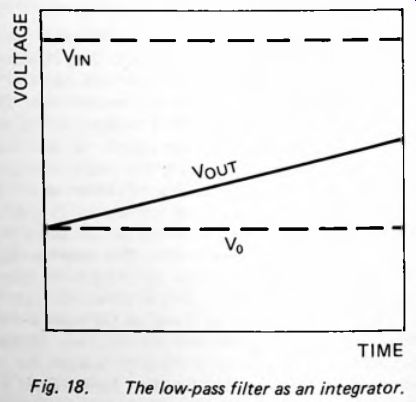
Fig. 18
For short consecutive periods of time, the filter integrates the input voltage during these periods. The low-pass filter can be thought of as an integrating circuit. Although the V_IN may be fluctuating widely, V_out shows only long-term changes.
Returning to the concept of filtering, the circuit is passing only the low-frequency components of the input signal. The circuit of Project 1 at the end of this section is an example that makes this function clear.
The converse applies to high-pass filters. In Figure 14, a sudden (i.e. high-frequency) increase of V_in results in a more-or-less equal increase in the voltage on the other plate of the capacitor. Before the next such pulse arrives, there is time for the excess charge to leak away through the resistor. Rout shows a short spike, as in Figure 19. The height of the spike depends on the rate at which Vin increases. In other words, V_out depends upon the rate of change of Vin. The filter is performing the mathematical operation of differentiation.
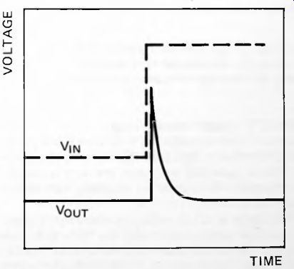
Fig. 19. Effect of input increase on a high-pass filter.
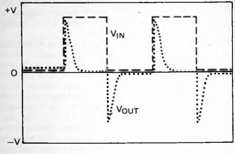
Fig. 20. Relationship between Vin and Vout when a high-pass filter receives
a square-wave input.
Figure 20 shows the effect of a high-pass filter when the input is a square wave. There is an upward spike coinciding with the beginning of each pulse and a downward spike at the end of each pulse (i.e. as V_in changes in a negative direction).
Returning to the original concept of filtering, the circuit is removing the low-frequency components of the signal and passing only the high-frequency components.
Level 1 or 3
PROJECT 1--Light-operated lamp
This circuit automatically turns on a lamp in a porch or room when the ambient light level falls below a given level. When the ambient light level rises again the lamp is turned off. The circuit can also be adapted for switching other devices such as buzzers, or motors.
If the lamp is of low voltage, powered by a battery or from a low-voltage mains adaptor, this is a fairly easy project for a beginner. BUT UNLESS YOU ALREADY HAVE KNOWLEDGE AND EXPERIENCE WITH WORKING WITH MAINS WIRING AND VOLTAGES, YOU SHOULD NOT ATTEMPT TO USE THIS CIRCUIT FOR SWITCHING MAINS-POWERED LAMPS OR OTHER DEVICES.
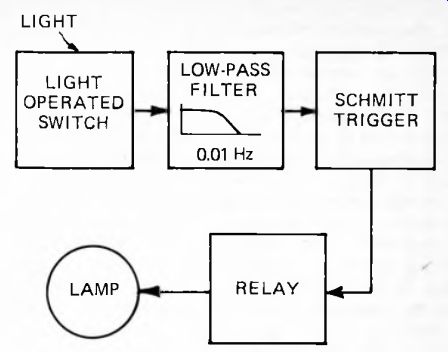
Fig. 21. System diagram of light-operated lamp.
How It Works
This is an example of the use of a filter to prevent unwanted signals from triggering the system. The system diagram (Fig. 21) shows that a light-operated switch circuit is used to detect the level of ambient light. The sensor is placed where it will be affected by daylight but unaffected by the lamp when it is on. The output voltage of the switch circuit rises with increasing light intensity. When the voltage exceeds a given level, the Schmitt trigger circuit operates the relay which turns the lamp on.
One of the problems with a circuit which depends upon light level is that of differentiating between the slow changes of level occurring at dusk and dawn, or by occasional excessive cloud, and the more rapid changes caused by other means.
Rapid changes may occur when small clouds pass across the sun. If the area is partly shaded by trees, the moving shadows of leaves being blown by the wind may bring about very rapid changes in the amount of light reaching the sensor. The shadows of persons or vehicles passing by, particularly when the sun is near the horizon, may also affect the sensor. At night, the headlights of passing vehicles may continually lead to changes in light level. This is the reason for the low-pass filter placed between the light-operated switch and the Schmitt trigger. It filters out rapid changes in the signal due to the effects described above. Conversely, it passes slow changes such as those occurring at dawn and dusk, or when the sky becomes clouded for significant periods of time.
A more detailed examination of the circuit (Fig. 22) shows that the light sensor is a light-dependent resistor (R1). There is no need for a fast-acting light sensor such as a photodiode in this application. The resistance of the LDR decreases with increasing light level. Together with VR1 it forms a potential divider. In the light, the resistance of R1 is low and the voltage at the junction of R1 and VR1 is high enough to provide a base current to TR1. This is turned on, causing the voltage at its collector to fall almost to 0V. The low voltage causes current to flow through the LED which lights. This serves to indicate the state of the light-operated switch. In the dark the resistance of R1 is high, the potential at the R1/VR1 junction falls and TR1 is turned off. The potential at its collector rises almost to +6V and the LED goes out. The exact light level at which the changeover between light' and 'dark' states occurs is set by adjusting VR1.
The effect of alternate light and dark periods is to produce an alternating signal at the collector of TR1. The low-pass filter consists of R5, R6, C1 and C2. The -3dB point for this filter is 0.01 Hz, equivalent to a period of oscillation of 100 seconds. The output of the filter rises or falls appreciably only when the input signal is high or low for periods of several seconds. This eliminates short-lived effects such as those mentioned earlier.
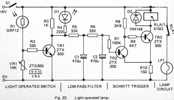
Fig. 22
The final part of the circuit, the Schmitt trigger, is intended to produce a sharp switching action. If the light level is low for long enough, the filter output rises very slowly. As it rises past a given level, a little over 3V, the trigger circuit changes state suddenly, de-energizing the relay coil. The relay contacts are wired so that they make contact, turning on the lamp.
Then if the light level is high for long enough, the filter output falls slowly. Owing to the nature of the trigger circuit, it does not change back to its former state until the voltage has fallen some way below 3V. The relay coil is energized and the contacts break, turning off the lamp.
Construction
If the circuit is to be powered by a battery, choose a case large enough to hold a high-capacity 6V battery, or a battery-holder for four 'D' cells. The circuit requires 20mA in the light, of which 10mA is taken by the LED. It is possible to economies in current by omitting D1 and R4 from the circuit, or by wiring a switch between D1 and the +6V line so that D1 can be switched out of the circuit when it is not being used for setting VR1 to the correct position. If the circuit is powered by a mains adaptor (6V d.c., 300mA) the case can be smaller and switch S1 is not required. The LDR can be mounted on the front of the case provided that it does not receive light direct from the lamp. If preferred, it can be mounted externally and connected to the rest of the circuit by a twisted pair of wires. VR1 can be a miniature preset potentiometer but it is likely that the triggering level may need to be adjusted from time to time to take account of seasons, in which case a panel-mounting carbon potentiometer ('volume control') is preferable.
Assemble the light-operated switch, including D1, and test its action. When VR1 is correctly adjusted, Dl is normally on but goes out when you shade the LDR. Add the filter circuit. Monitor the output at the junction of R6/C2, using a voltmeter. When power is switched on, the voltage is low and remains low. When the LDR is shaded the voltage increases very slowly. It is clear that the current passing through R3, R5 and R6 is slowly increasing the charge on the capacitors.
This is a very clear illustration of the way in which a low-pass filter also acts as an integrator. Here we are integrating the output of the light-operated switch over a prolonged period of time.
Complete the wiring. Figure 22 shows the lamp LP1 and the relay contacts RLA1 wired to the +6 and 0V rails. This is for controlling a 6V filament lamp. Alternatively, they may be wired to a completely separate power source, for example a 12V lead-acid rechargeable battery. The mains can be used as a power source, provided that the relay contacts are rated to withstand mains voltages and currents. If the mains is used great care must be taken that there is no possibility of any connection between the relay contact circuit and the other parts of the circuit. You should attempt this only if you have had previous experience with wiring such circuits.
The correct setting for VR1 is established at a time when the ambient light is at the level at which switching is to occur.
Turn VR1 so that the LED is glowing at approximately half its maximum brightness.
Special Components
Resistors:
ORP12 or similar light-dependent resistor (= cadmium sulphide cell)
R1
Semiconductors:
light emitting diode 1N4148 silicon signal diode TR1-TR3 ZTX300 npn transistor (3 off)
D1
D2
Miscellaneous:
RLA/1 for low-voltage operation, this can be a miniature or sub-miniature pcb mounting relay; for mains operation a larger type is required with contacts suitably rated. In either case the coil is rated at 6V and it has single change-over contacts.