AMAZON multi-meters discounts AMAZON oscilloscope discounts
The idea of a notch filter, or frequency rejection circuit was first mentioned in connection with one type of band-pass filter. In essence, the notch filter is the converse of a band-pass filter for it passes all frequencies except for those in a relatively limited band. One common application of the notch filter is to remove interference at mains frequency (50Hz) from audio circuits and from circuits used in medicine for monitoring low-frequency signals from the human body.

Fig. 55. Twin-T notch filter.
Figure 55 shows a passive notch filter, the twin-T filter, which has already been seen as part of the circuit of Figure 46.
The center frequency of this circuit is f0 = 1/ pi RC. This is the frequency at which the signals passing along the two networks become 180° out of phase with each other and therefore cancel out.
Because of the cancelling-out effect, the response curve of a passive notch filter shows a distinct and narrow dip at, and close to, the center frequency. At frequencies on either side of the centre, the slope the curve flattens out rapidly. In other words, bandwidth is relatively wide. There is also the problem that the performance of the filter depends very much on the precision of the values of the three resistors and three capacitors. Finally, it is not easy to build a tunable notch filter of this type owing to the difficulty of obtaining a triple-ganged variable resistor with the right combination of resistances.
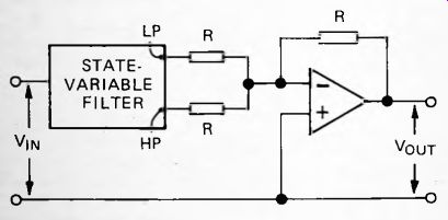
Active notch filters have better responses than passive filters and can be built from state-variable filters of the type shown in Figure 48. If we take the low-pass output from a state-variable filter and add it to the high-pass output, the resulting response has its lowest point at the cut-off point.
This is at the frequency at which the signal from the low-pass and high-pass outputs are exactly 180° out of phase (page 82). Figure 56 shows the state-variable filter with its high-pass and low-pass outputs being summed by an op amp, wired as a summer (compare Figure 49). Figure 57 shows a typical notch response obtained from this kind of filter.

Fig. 56. An active notch filter, based on a state variable filter and an op
amp.

Fig. 57. Response of an active notch filter.
To make a tunable notch filter we base it on a tunable state-variable filter. We begin with a design such as Figure 51, replacing the variable or switchable components with fixed-value components for those parameters which we do not wish to vary. With an appropriate pair of capacitors permanently wired in, the frequency can be swept over a 10:1 range by simply using the dual-ganged variable resistor (VR2/VR3). Dual-ganged variable resistors are relatively easy to obtain.
The filter just described is manually tunable, but there are many applications in which the filter must be electronically tunable. For this purpose we require an electronically tunable state-variable filter. Below we examine a filter of this type, which is used to build the notch filter for Project 7 at the end of this section. Another type of electronically tunable filter is described in Section 9.
Switched-capacitor Filters

Fig. 58. The principle of the switched-capacitor filter.
This is a different type of active filter, based on the principle illustrated in Figure 58. Two capacitors and two switches are connected as shown. The switches are under the control of a clock circuit that operates at high frequency, usually several kilohertz. The clock opens and closes the switches alternately.
When S1 is open, S2 is closed, and the other way around.
Obviously the switches used in this filter can not possibly be ordinary mechanical switches. They are transistor switches, usually field-effect transistors of the type referred to as analog switches. They are controlled by receiving a logical low or logical high input from the clock. When the input is high the switch is 'on' and, in effect, becomes a low-value resistor. Its resistance is in the order of 100 ohm, offering minimal resistance to the flow of current. When the switch receives a low input it is 'off' and its impedance is very high, virtually preventing the flow of current.
The way the circuit works is as follows. Suppose that, at a given instant, the value of the alternating signal is Vx. S1 is 'on' and S2 is 'off'. Current flows through S1 and charges C1 until the voltage on C1 is Vx. We are assuming that C1 has capacitance Cx small enough to allow it to charge fully to Vx during the short time that SI is 'on'. Now S1 is turned 'off' and S2 is turned 'on'. What happens next depends on what charge is already present on C2. Suppose that the voltage across C2 is V2 and that V2 is less than V1. Current flows from C1 to C2 until both capacitors are charged to the same voltage, intermediate between Vx and V2. Similarly, if V2 is greater than Vx the capacitors share their charge, and come to the same voltage, though in this circumstance the current flows from C2 to C1.
The charge on C1 starts as Cx Vx (charge = capacitance x voltage) and the charge on C2 starts as C2 V2. When S2 is closed the total charge is shared between the capacitors, and they finish up with equal voltages across them:
C, V, + C2V2 total charge
Final voltage =total capacitance C1+C2
This final voltage passes to the op-amp, wired as a voltage follower, so this is the value now taken by V_out--The important point about this sequence of events is that there is a leveling effect. If is rising, each sample of V_in (taken when S1 is on) is averaged out against the effects of preceding smaller samples (V2). This tends to flatten out the rise in V_in and so V_OUT voltage are converted to slower changes of output voltage.
Slower changes of voltage are less affected. In other words, the circuit acts as a low-pass filter, in which low-frequency signals are passed more readily than high-frequency signals.
The action of this circuit is affected by the rate at which the switches are turned on and off, i.e. by the clock frequency.
If the clock runs fast, there may not be sufficient time for the capacitors to charge fully. This is equivalent to putting extra resistance into the circuit. The frequency response of the low-pass filter thus depends on the clock rate. It is a frequency-controlled filter. This is a very useful property for, in its turn, the clock rate can be controlled by an external voltage. Together the clock and filter become a voltage-controlled filter, or VCF.
Switched-capacitor filters have the advantage that they are easy to build. Integrated circuits are available that have all the major components for two second-order state-variable filters, including the capacitors, on a single chip. The popular MF10 filter IC has the three essential building blocks, the summer and two integrators, in switched-capacitor form. It contains two sets of these blocks so two separate second-order filters can be built. The two filters can be cascaded to produce a fourth-order filter using a single IC. All that the user needs to provide is the clock circuit or circuits to set the cut-off frequency of each filter. Also required are a few resistors to set the gain and Q of the filter. By suitably joining the various parts of the integrated circuit it is possible to build low-pass, high-pass, band-pass and other types of filter. The filter can be shows a slower rise. Conversely if V_in is falling, V_OUT falls too, but at a slower rate. Rapid changes of input tailored to give all the well-known responses, including Butterworth, Bessel and Chebyshev.
One point to note is that, since the filter works by a switching action, its output is not exactly the same as that which is obtained from a more conventional resistor-capacitor passive or active filter. The output varies step-wise, not smoothly. In effect the switching action adds a high-frequency component to the signal. Provided that the clock frequency is much higher than the frequencies present in the original signal, this is of no consequence. But switched-capacitor filters are unsuited for use with high-frequency signals.
Transmission-zero Filter
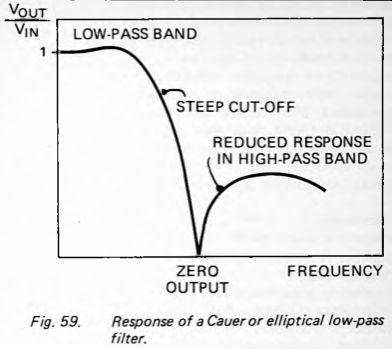
This is a variation on the notch filter. In Figure 56 the signals from the low-pass and high-pass outputs are mixed in equal amounts to produce the notched response. We can also mix them in unequal amounts to obtain other responses. In the notch filter the signals flow to the op amp through two identical resistors but, if the resistors have different values, the signals are weighted so that one or the other of the signals predominates in the output from the op amp. All kinds of mixes of the HP and LP signals are possible but one that is of special interest is obtained when we leave the LP signal unchanged and reduce the proportion of the HP signal. This is done by increasing the value of the resistor between the HP output and the op amp.
Taking the extreme case, if there is infinite resistance between the HP output and the op amp, the signal from the op amp is simply the LP signal. Beyond the pass-band the signal level slopes down gently at -12dB per octave (as in a first-order filter). If we mix in a relatively small amount of the HP signal, the effect is to steepen the roll-off curve beyond the LP pass-band (Fig. 59). This type of filter, also known as a Cauer or elliptical filter, could be called a 'lop-sided' notch filter. It has a notch but, on the high-frequency side of the notch, the signal level is 10 or more decibels lower than on the low-frequency side. On the other hand, if we ignore the high-frequency response, we can look at this as a low-pass curve that falls off much more steeply than -12dB octave. The rate of fall can be adjusted by mixing in a suitable proportion of the high-frequency signal. In this way we can produce a low-pass filter with very steep cut-off. The only reservation is that the higher frequencies are present, even though at a relatively low level so, if this raises difficulties, this type of filter can not be used.
A high-pass Cauer filter is made by selecting the resistors so that the high-pass signal dominates the mixture.

Fig. 59
PROJECT 7--Phaser
Level 2--A phaser is a device used to modify the sound coming from an electronic musical instrument such as an electric guitar.
The result is hard to describe in words but is easily recognizable when heard, and is a popular musical effect. There are a number of ways to produce the effect and in this circuit we make use of a pair of notch filters built around the MF10 switched capacitor filter IC.
The basis of the action of the phaser is the 180° phase change that occurs in a state-variable filter, causing the signal to be notched out at a given frequency when the low-pass and high-pass outputs are mixed (see above). A phaser circuit varies the notch frequency regularly, sweeping up and down over the audio spectrum, so producing the characteristic phaser sound. The effect is made more striking by having several notch filters, with their center frequencies spaced a little way apart, all being swept simultaneously. This project has two notch, filters, but it would be easy to extend the circuit to four filters by adding another MF10 IC.
How It Works
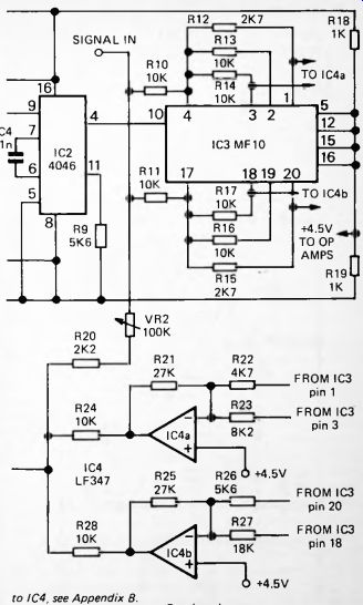
The circuit consists of four main sections: sweep generator (Fig. 60, IC1), voltage-controlled oscillator (IC2), filters (IC3) and mixers (IC4).
The sweep generator is based on the same IC as the audio signal generator (Project 5). In fact it is easy to modify Project 5 to this end. The main change is to increase the value of the timing capacitor from 200nF to 10 uF so that it operates as a low-frequency oscillator. It is also an improvement to alter the values of VR1 and its associated fixed resistor so that the frequency of the oscillator may be varied from about 0.2Hz to 10Hz. This controls the rate at which the phasing effect is swept across the audio spectrum, the sweep frequency. The square-wave output of IC1 is not required in this application.
IC2 is a phase-locked loop IC, although we use only the VCO part of it in this circuit. The VCO generates the square-wave clock signal that determines the center frequency of the filters. The frequency of the VCO, the clock frequency, f_cLK, depends upon the voltage that IC2 is receiving from IC 1.
With a triangle wave output, the voltage ramps up and down between 3V and 6V at the sweep frequency. When the voltage is 3V, f_clk is about 30kHz. When the voltage is 6V it is about 140kHz. When switched to the sine wave output the sweep frequency ranges between 50kHz and 120kHz. It is possible to lower the sweep range by altering the capacitance of C4 to 2.2nF, should the constructor prefer the effect produced by a lower range.
The resistors connected to IC3 have been chosen so as to give a relatively low gain, to minimize distortion and a low Q to minimize resonance.
Both filters have the same set of resistor values so their outputs are identical. It is the mixing of the LP and HP outputs which produces the two different notch effects.
These depend on the relative values of the resistors feeding the two op amps, IC4a and IC4b. For IC4a, the notch frequency is:

--------
When the clock is swept from 30kHz to 140kHz, the notch frequency is swept from about 400Hz to 1800Hz. This is for triangular waves. The range is less when using the sine-wave output of IC1. For IC4b, the notch frequency is swept from 540Hz to 2500Hz. Between them, the notches sweep across the most-used parts of the musical scale, including the lower harmonics.


Fig. 60. Project 7: Phaser. For optional connections to IC4, see Appendix
B.
Continued

Fig. 61.

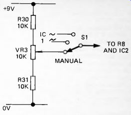
Fig. 62. Optional manual sweep control.
The third mixer, IC4c mixes the two notched signals in equal proportions and permits the addition of the original unfiltered signal. By adjusting VR2 the proportion of the original signal can be increased so as to more-or-less swamp the phaser effect, or decreased so that only the phaser signal is heard. The output from IC4c is fed to a high-power audio amplifier. Use a ready-made unit or build one from the many kits available. Figure 61 gives a circuit for a simple audio power amplifier which can be used with this project as well as with other audio projects later in the guide.
The controls for this project are summarized as follows:
Sweep-rate (VR1): from 0.2Hz to 10Hz
Depth (VR2): from no phasing effect to maximum effect
Waveform (SW1): triangular (the most distinctive effect) or sine wave (softer, with less wide sweeping).
An optional extra control is manual sweep. This consists of a variable resistor, connected as in Figure 62 with a third position on switch SI to select either automatic or manual action.
Construction
The circuit requires about 25mA (excluding power to drive the audio amplifier), which can be provided by a 9V PP3 battery or a mains adapter. Because of the conditions under which the project is likely to be used, the circuit should be housed in a stout metal enclosure. If the case is connected to the OV line this will reduce the pick-up of hum from nearby electrical equipment. For use with certain instruments it is preferable for the sweep-rate to be controllable by foot. A foot-pedal which incorporates a 100 k-O variable resistor is ideal for this purpose, to replace VR1. An alternative, or possibly additional foot control is a switch inserted into the line between R11 and VR2. This allows the switching in or out of the phaser effect. This could have either a latching or non-latching action, as preferred, The foot-switch or switches are mounted on top of the enclosure, or a freestanding foots-well pedal may be used for VR1.
The enclosure requires two jack sockets, one for input and one for output. Usually the input socket is wired so that pushing in the jack plug turns on the power supply to the circuit.
When constructing the unit there is scope for using different resistance values to vary the effect. The resistors shown in Figure 60 produced the best effect in the opinion of the author, but this is a field in which personal taste plays a large part. The resistors which could be experimented with are R12, R13 and R14, particularly R12. The corresponding resistors on the other filter can be altered to match the chosen values or be given a different set of values. These resistors all affect the quality of the filtered sound, particularly in emphasizing either the treble or bass response. R22, R23, R26 and R27 are concerned with the mixing of LP and HP signals. In general R23 should be larger than R22 and R27 should be larger than R26.
Special Components
Resistors
Carbon resistors, 0.25W with 5% tolerance are suitable. VR1 is shown with a logarithmic track for preference, though a linear track is also suitable. VR2 has a linear track.
Capacitors
Polyester or polystyrene capacitor
C4
Integrated Circuits
8038 function generator
4046 CMOS phase-locked loop
MF10 dual switched-capacitor filter
LF347 quad JFET op amp
IC1
IC2
IC3
IC4
The Audio Amplifier
Resistors are 0.25W, except for R6, which is a 2.5W wire-wound resistor. The input lead should be screened, with the screening connected to the 0V line. A compact layout helps avoid interference, except that the input and output sides should not be close together. C4 and C5 are mounted with their terminal wires soldered as close as possible to pins 3 and 5 of the IC. The IC requires a small bolt-on heatsink, rated at about 20°C/W. The loudspeaker must be rated at a minimum of 10W. A multiple speaker unit can be used.