The ICM7555 and ICM7556 Timers
One of the easiest ways to create an oscillator circuit is with an ICM7555 timer IC. This chip is so useful for oscillator design that it is worth taking a little time to understand its internal structure and operation in detail. A thorough grasp of this will allow the enthusiast to create endless ingenious oscillator circuits using a minimum of additional external parts.
The prefix "7" indicates that this is the CMOS "micropower" version of the device, which offers some significant advantages over its older bipolar stable-mate. To begin with it draws much less current from the power supply and can operate from lower voltages. Supplies from as low as three volts up to a maximum of fifteen volts can be used with a typical drain of around a hundred microamps, making this the ideal choice for battery powered circuits. When lightly loaded the output voltage swings practically all the way to both supply rails, a feature which can greatly improve frequency stability in many oscillator designs. Input impedances are much higher than those of the bipolar version, allowing the use of small capacitors together with high resistance values in low-frequency circuits. Finally, it doesn't need the local "decoupling" capacitors for the supply and "control" connections required by the bipolar type, although as always there should be some decoupling included in the circuit. One word of warning; being CMOS, the ICM7555 is rather prone to damage by static, so experimenters are advised to take suitable precautions such as the use of an earthed wrist strap when handling this chip.
A simplified version of the ICM7555 internal construction is shown in Figure 1.1. It has two inputs, "trigger" and "thresh old", which go to a pair of internal comparators. The other two comparator inputs are provided with reference voltages of one third and two-thirds of the supply voltage from an internal chain of three identical resistors, and their outputs go to the "set" and "reset" inputs of a flip-flop which drives the output.
The flip-flop also drives a "discharge" transistor with an open collector, intended for discharging the capacitor used in timing circuits. In these CMOS versions of the device this is, of course, the drain of an FET. The "control" input is a direct connection to the upper reference voltage and can be used to force this higher or lower. This affects both reference voltages of course, but it alters the higher one by twice as much as the lower so it can be used for frequency adjustment. There is also a "reset" input, not shown in Fig.1.1, which forces the flip-flop into the "reset" state if taken low. In most oscillator circuits this is not needed so it is disabled by direct connection to the positive supply.
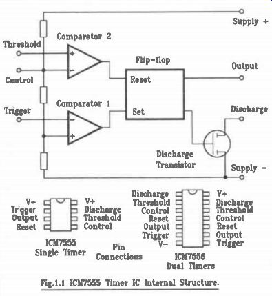
Fig. 1
The IC operates as follows. If the voltage at the "trigger" input falls below a third of the supply voltage, the output of comparator I goes high, "setting" the flip-flop. This causes the output to go high (positive) and the discharge transistor to be turned off. If the "threshold" input voltage now rises above two thirds of the supply the flip-flop is reset, with the output going low (negative) and the discharge resistor being turned on. In oscillator applications, the two inputs are often connected together and used as a single input so that the circuit becomes a "Schmitt" device with accurate thresholds. It should be noted that this "inverts" the input voltage, with the output going high for an input below the lower reference and low as it rises above the upper one.
The ICM7555 is available in the common 8-pin DIL package and there is also a dual version, the ICM7556, with two timers contained in a single14-pin Dri, package. Pin connections for both are shown in the drawing. They can operate at frequencies up to about 500kHz and with their high input impedance and reasonable output drive capability it can be seen that these cheap and readily available ICs can be used in an unlimited variety of oscillator designs. In the next few pages some of these will be described.
The Basic ICM7555 Oscillator Circuit
Figure 1.2. shows the standard "astable" oscillator circuit for the ICM7555 timer. This is the basic circuit that is shown in most component catalogues and other sources of 555 IC information. In operation, capacitor C1 is charged and discharged repeatedly between the internal reference voltages of one third and two-thirds of the supply voltage. During the charging part of the cycle current flows into the capacitor from the positive supply through R1 and R2. The output, from pin 3, is high (positive) and the discharge transistor's drain, pin 7, is "off". This state continues until the voltage across C I reaches two thirds of the supply, when the internal flip-flop changes state, the output goes low (negative) and the discharge transistor is turned on. The drain of this transistor now pulls pin 7 down almost to the negative supply potential. The current from R1 is now diverted into pin 7 and C1- begins discharging into it through R2. Discharge continues until the voltage across C 1 has fallen to one third of the supply voltage when the flip-flop state is again changed, turning off the discharge transistor and driving the output high, and the whole cycle repeats.
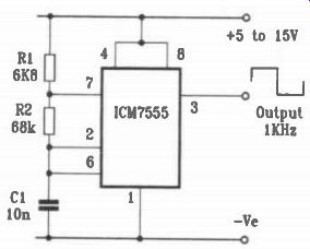
Fig.1.2 Basic 1CM7555 Oscillator Circuit.
The charging and discharging of the capacitor is exponential in nature, but for a change of one third of the supply voltage with an effective starting voltage of two-thirds of the supply, the time, or period, of each half cycle is very nearly 0.7 x R x C. Of course, "R" for charging is RI+R2 whilst "R" for discharging is just R2, so the total period per cycle can be calculated from:
t = 0.7 x (R1+(2 x R2)) x C1 seconds.
and the frequency, which is always lit, is therefore:
f = 1
0.7 x (R1+(2 x R2)) x C1 Hz.
The values in these formula are, like all those given in this guide, expressed in ohms, farads, seconds and hertz so the necessary compensation should be made in calculations to allow for this. With the values shown in Figure 1.2 the output will be about 1-kHz but frequencies can be from many seconds per cycle up to 500kHz and perhaps more. At high frequencies the effects of stray capacitance and internal propagation delays usually result in a lower frequency than calculations might suggest so a little practical testing is advisable. The capacitor value can be from a few tens of picofarads to many microfarads and, as the device has the very high input impedance typical of CMOS, resistors can have values from around 4k7 up to 10 megohms or more. Although ICM7555 oscillator circuits are sometimes seen using electrolytic capacitors for "C" this is not really recommended. The wide manufacturing tolerance allowed in electrolytic capacitance values together with their unpredictable leakage currents makes them generally unsuitable for timing or frequency control. Where a low frequency is required it's better by far to use a CMOS divider, a technique which will be covered later in this guide. Ceramic capacitors are also best avoided where stability is important because their values often change significantly with temperature. Polyester, polystyrene and silver-mica types are best.
An advantage of this circuit is that the output is not part of the frequency generating network so loads connected to it have no effect on the frequency. With the old bipolar type of 555 small loudspeakers were often driven directly by the output. Whilst the CMOS version doesn't have the power for this it can drive piezo transducers very effectively, and a simple buffer circuit could be used for higher power. Because the switching points and the charge-discharge rates are proportional to the supply voltage, variations of supply voltage have virtually no effect on frequency.
There are some disadvantages with this circuit. It cannot generate a true "squarewave" output. Because of the different values of resistance present in the charge and discharge portions of the cycle the charging time will always be longer than the discharge time, so the output can never be symmetrical. If something approaching a squarewave is required R1 will have to be small in comparison with R2, which raises the current through R1 during the discharge cycle, increasing the overall consumption and the saturation voltage across the discharge transistor. This may adversely affect frequency calculations, already complex because of the two resistance values. There is another arrangement,. which for many applications may be better, as will be seen in the next circuit.
Components for Figure 1.2
Resistors (metal film, 0.6W) R 1 6k8 R2 68k Capacitor C1 10-nF polyester
Semiconductor
IC1 CM7555 CMOS timer.
Alternative ICM7555 Oscillator Circuit
A glance at the circuit of Figure1.3 will show how much simpler this is compared to the previous arrangement. Just one resistor and one capacitor are used with the ICM7555 to create a stable and reliable oscillator with an output that is a true squarewave. The operation is simpler to follow, too. Whilst the output of the IC is positive it charges the capacitor C1 through resistor R1. When the voltage across C 1 reaches two-thirds of the supply the IC output changes state, going low and discharging C 1 through R 1. When the capacitor voltage has dropped to a third of the supply, the IC output again changes state and the cycle repeats.
The calculations are easier too. Each half cycle is still calculated from 0.7 x R x C, but there is now only one value of R to consider, so the total period is given by: t=1.4xRxC
and the frequency, the inverse of this, is given by:
1/f - (1.4 xRxC).
This is much simpler than the formula for the previous circuit.
The component values shown result in a frequency of about 1050Hz, but like the previous circuit this arrangement can operate at frequencies up to around 500kHz.
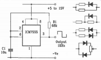
Fig.1.3 Alternative ICM7555 Oscillator Circuit.
This circuit doesn't work so well with the bipolar type of 555 IC but with the CMOS ICM7555 version performance is excel lent. The output has a near-perfect 50-50 duty cycle, the frequency is substantially stable right across the supply voltage range and the current consumption is smaller, making this a better choice for battery operation. Frequency trimming is simple too. A variable resistor can be used in series with the fixed one to give the required range of adjustment. If a non symmetrical output is needed this can be obtained by using one or more diodes to alter the effective resistor values for charging and discharging the capacitor. Any of the networks shown to the right of the circuit can be used in place of resistor R1 to achieve this. The top two examples both produce shorter positive output half-cycles, reversing the diode would shorten the negative ones. The third network gives independent control of each half-cycle, whilst the last provides duty cycle variation that is practically independent of operating frequency. A practical application for this might be in simple power control, such as a cavers' lamp with variable brilliance to conserve battery power.
This is a good point to pause and explain a disadvantage of frequency adjustment with a variable resistor in this type of circuit. It is actually the oscillator period that is directly proportional to the resistance value, not the frequency. The frequency, as shown in the above formulae, is inversely proportional to the period. In practice this means that frequency controls spanning ratios greater than about five to one will have most of their control range hopelessly compressed into one end of the scale.
One way around this problem is to use a multi-way switch with suitable fixed resistor values for each frequency step, but if a smooth linear control is needed over a large range, the circuit of Figure 1.7 will show how this can be achieved.
The advantages of this circuit are its simplicity, ease of use, better output symmetry and lower power consumption. When using it though, the limitations of the ICM7555 output should be kept in mind. It will only swing all the way to the positive and negative supply rails if the loading on it is kept light. Also, its drive capability is not symmetrical, it can sink a lot more current to negative than it can source as a positive output so overloading is likely to cause loss of output symmetry. The value of resistor RI should therefore be kept reasonably high, not less than 10k. To obtain an output without loading it there are several options. The circuit being driven may have a high enough impedance input in any case. CMOS gates can be driven without problems, in fact one could be used as a buffer.
The "discharge" connection at pin 7 is not used by this circuit, which creates some interesting possibilities. To avoid output loading the signal can be taken from this instead, using a "pull up" resistor to the positive supply. This could provide a TTL compatible output with the pull-up resistor connected to the TTL's 5-volt positive supply. A variable DC voltage might be applied to the pull-up resistor, resulting in an output with the frequency of the oscillator but having an amplitude directly proportional to the applied voltage. This could doubtless find some really interesting applications. Finally, an ICM7556 dual timer might be used, with the inputs of the second timer connected to the output of the first to create a buffer.
Components for Figure 1.3
Resistor R1 68k metal film, 0.6W
Capacitor
C1 10nF polyester
Semiconductors
Diodes
Any small silicon signal type, 1N4148 etc.
ICI ICM7555 CMOS timer.
Voltage Controlled Oscillator
Now that the basic ICM7555 oscillator circuits have been covered, some more interesting circuits can be described.
Voltage controlled oscillators are frequently needed by circuit designers, and are often designed around 555 timer ICs. The method generally used is to charge the timing capacitor with a voltage-controlled constant current, often from a transistor, and discharge it with the internal transistor in the timer. The output from this type of circuit is a stream of pulses of constant width, with the time between them being voltage controlled. This arrangement has a couple of disadvantages. The charging current must come from the positive supply so the control voltage must be relative to this and become increasingly negative for an increase in frequency. Control signals are usually relative to negative supply however, and positive-going, so a "current mirror" circuit is needed. The other problem is that the output pulses from this version of the circuit are negative, but many designs work better with positive pulses. A circuit having neither of these drawbacks is shown in Figure 1.4.
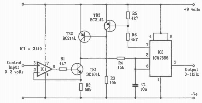
Fig.1.4 Voltage-controlled Oscillator Circuit.
This circuit is the reverse of the version described above. The discharge of capacitor C1 is voltage controlled, with short charging pulses controlled by the discharge transistor of IC2.
To follow the operation, assume that the output from pin 3 of timer IC2 is low and the discharge transistor pin 7 is on, drawing current through R6 to turn on transistor TR3. This transistor holds the base of TR2 at the positive supply potential, ensuring that it is off. The capacitor C1 can therefore discharge through R4 at a rate determined by the collector current of TR1.
As the voltage across it falls to a third of the supply voltage, the timer output goes high. At the same time the discharge transistor and TR3 turn off, so current from R3 now turns on TR2, which charges CI through R4. When the voltage across C1 reaches two-thirds of the supply voltage, IC2 again changes state and the cycle recommences.
A characteristic of transistors is that nearly all the current flowing into the emitter flows out again from the collector. A minute part flows out through the base, but this is usually so small it can be ignored. Since the emitter voltage follows the voltage applied to the base, less the "base-emitter drop" of about 0.6 volts, this can be used to control the voltage across the emitter resistor, R2 in this circuit. The base voltage there fore controls the current from the collector, creating a voltage controlled current source. The control voltage can be applied directly to the base of TR1 to control the frequency in this circuit, but if an op-amp is used with the transistor as shown the voltage across R2 will correspond almost exactly to the input voltage, with the op-amp automatically compensating for the emitter-base voltage drop and variations of this with tempera ture. The resulting output frequency control range will then start from zero instead of 0.6 volts.
Design calculations for this circuit are a little more complex than those for the simple fixed-frequency circuits and a few design rules have to be observed. R4 should be fairly low in comparison with R2. There must always be enough voltage across TR1 for it to operate, so the input should never exceed a value of about a volt below a third of the supply. This circuit is sensitive to supply voltage changes, so the supply may have to be regulated. Once it has been decided what the maximum control voltage is going to be, the period for the discharge part of each cycle can be calculated from: CxRxE t = V Where C is the value of the timing capacitor C1, R is the value of emitter resistor R2, E is a third of the supply voltage and V is the voltage across R2. To this should be added the time for the charging part of the cycle:
t=0.7xC1xR4
These two together give the total period per cycle so, as always, their inverse gives the corresponding frequency. With the component values shown and a supply of 9 volts the circuit generates a frequency output from zero to about 1 kHz for an input of 0 to 2 volts. The output consists of positive pulses of about 1001 is width, ideal for making lots of noise with a small loudspeaker with the simplest of output buffers, perhaps a single transistor. With a in capacitor for C 1 it produces just over 9 kHz for the same input voltage range, with correspondingly shorter output pulses. Note that if an op-amp is used as shown it must be of a type with inputs and output capable of operating down to the negative supply potential. The CA3140 shown is suitable, other possible are the CA3130, or one of the amps in a CA3240, an LM358 or an LM324. Other transistors can be used in place of the types shown, so long as they are of correct polarity.
The usefulness of this circuit is limited mainly to audio work, but is cheap, simple and fairly stable.
Components for Figure 1.4
Resistors (all metal film, 0.6W)
R1 4k7 R2 56k R3 10k R4 15k R5 4k7 R6 4k7
Capacitor
C1
Semiconductors
IC I IC2 TR 1 TR2 TR3 10n polyester
CA3140 op-amp ICM7555 CMOS timer BC184L BC214L BC214L
Voltage Controlled Oscillator
Using ICM7556 In the last circuit, transistors were used for generating a constant current and for inverting the discharge output from a timer IC in the design of a voltage controlled oscillator circuit. To demonstrate the possibilities, here's a completely different approach to VCO design with an op-amp integrator replacing the timing capacitor and current source and an ICM7556 dual timer providing the inversion.
An op-amp integrator has two inputs, a non-inverting one which is usually connected to a reference voltage, and an inverting one to which an input voltage is connected through a resistor with negative feedback from the output applied through a capacitor. Within the constraints of supply voltage, the op amp uses the feedback to keep the voltage at the inverting input equal to that at the non-inverting one. This means that if a steady voltage is applied to the input resistor the potential across it will be the difference between this and the reference voltage so a constant current flows into the input as a result.
The feedback capacitor is charged by this current, so to keep the inverting input voltage constant the op-amp output voltage changes at a constant rate. This can be used to design an oscillator, switching the input voltage polarity as the output passes the input thresholds of a timer IC. One minor difficulty is that the integrator output is inverted, falling for a positive input and rising with negative. To make a workable oscillator with the inverting ICM7555 there must be a polarity reversal at some point. One way to do this is with a dual op-amp, with the second inverting the output of the first. This requires at least two more resistors however, and can limit the frequency of the circuit. A better approach is to use a dual timer, with the second acting as an inverter for the output of the first.
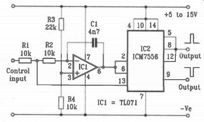
Figure 1.5
Figure 1.5 shows a circuit that operates in this way. IC1 is the integrator, with a reference of about a third of the supply voltage applied to its non-inverting input, pin 3, by resistors R3 and R4. Whilst the discharge transistor of the second timer, pin 13, is off, a voltage greater than the reference applied to resistor R1 will cause the output of IC1 to decrease at a rate determined by the input voltage and the values of R1, R2 and capacitor C1.
When it reaches a third of the supply voltage, the first timer changes state with its output, pin 5, going high. This is connected to the inputs of the second timer, pins 8 and 12, so the output of this now goes low and its discharge transistor, pin 13, turns on. The integrator now has an effective negative input of about a third of the supply connected to R2, so its output starts to rise. When it reaches two thirds of the supply voltage the two timers change state again and the cycle repeats.
The time for the first part of the cycle is given by:
CxRxV t = E Where C is C1, R is R1 + R2, V is a third of the supply voltage and E is the applied input voltage.
The time for the second part of the cycle can be determined by a similar formula, but in this case R is R2 alone and V and E are approximately equal in value, so the time is given simply by: t=C1 xR2.
As with the previous circuit, these two can be added together to obtain the total period for each complete cycle, and the inverse of this gives the frequency. The values shown produce 50ms pulses with a frequency of 10kHz for an input equal to the supply voltage.
This is an easier circuit for experimenters to work with than the previous one. The input voltage may be equal to or even higher than the positive supply. Higher frequencies can be reliably achieved, so long as a suitably short output pulse width is set with R2 and C1. The fact that the control voltage must be higher than a third of the reference might be a disadvantage but this can be offset elsewhere, perhaps by a resistor between the input and the positive rail. The output point shown, from pin 5, consists of positive pulses but negative ones are also available from pin 9 and the discharge transistor of the first timer, which is off during output pulses, is also available at pin 1. The op amp does not have to be a type able to operate with inputs and output at negative supply potential like that of the previous circuit, the TL071 shown was found to work particularly well in this arrangement. The main disadvantage is perhaps the extra cost of the dual timer, but the circuit uses fewer components and is simpler to construct than the transistor version.
Components for Figure 1.5
Resistors (all metal film, 0.6W )
R1 10k
R2 10k
R3 22k
R4 10k
Capacitor
C1 4n7 polyester
Semiconductors
ICI TL071 op-amp, FET input.
IC2 ICM7556 dual CMOS timer
Simple Triangle Wave Generator
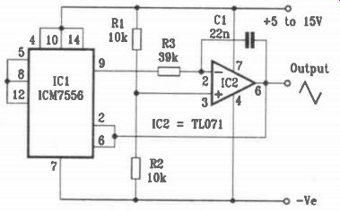
Figure 1.6
Now that the use of an integrator and dual timer as an oscillator has been described, it is worth looking at a few more circuit configurations using these A very simple circuit can be constructed with a dual timer and an op-amp integrator to produce a signal with a triangular waveform. The circuit for this is shown in Figure 1.6. This again uses the ICM7556 dual timer IC to make a "non-inverting" timer for use with an inverting integrator. The difference is that here the input to the integrator is taken from the timer output and its reference voltage is set by R1 and R2 to half the supply voltage. Equal and opposite input voltages are therefore applied to the integrator input depending on the timer output state, so its output increases and decreases at the same rate in both directions. Note that this would not be the case with the older bipolar type of 556 timer, where the output does not switch all the way to both supply voltages like that of the CMOS micropower version. As the timer output changes state as the integrator output reaches one third and two thirds of the supply voltage, the triangle wave always has a peak-to-peak amplitude of one third of the supply.
The frequency of this circuit is determined entirely by the values of R3 and C1 and is virtually independent of the supply voltage. The period for half a cycle is given by 0.667 x R x C, so the overall period is twice this:
t=1.333xRxC
giving a frequency of:
f= 1.333 xRxC 1
As always, stray capacitance and propagation delays can cause performance to differ a little from calculated values especially at higher frequencies, so practical testing should be carried out before finalizing circuit design. With the values shown the circuit produces an output of about 1-kHz, but it has been tested with the op-amp shown at frequencies well in excess of 100kHz and there was very little visible distortion of the triangular waveform. The output, as it is taken from the output of the op-amp, has a relatively low impedance. Loads as low as 100 ohms can be driven easily.
In addition to the triangular waveform, squarewave outputs are available from pins 5 and 9 of IC1 although these should not be loaded too much. The two discharge outputs from pins 1 and 13 are also available if required.
This circuit shows just how simple it can be to construct a reliable oscillator with an ICM7556 and very few external parts. In the next circuit a version with linear frequency control will be shown.
Components for Figure 1.6
Resistors (all metal film, 0.6W)
R1 10k
R2 10k
R3 39k
Capacitors
C1
Semiconductors
IC1
IC2
22nF, polystyrene or polyester.
ICM7556 dual timer, CMOS version.
11071 JFET input op-amp.
Variable Frequency Triangle Wave Generator with Linear Control
During the description of Figure 1.2, it was explained that the "period" of a simple 555 oscillator circuit was linearly related to the resistor and that if this was made variable with the object of providing frequency adjustment, the scale of the resulting control would have most of its range compressed into one end.
For applications requiring a linear frequency control the circuit of Figure 1.7 can be used instead.
The operation of this circuit is similar to that of Figure 1.6, using an ICM7556 dual timer connected as a "non-inverting" timer for use with an inverting integrator configured from IC2b.
However, instead of being connected directly to the output of the timer as before, the input to the integrator, to resistor R4, is first attenuated by the variable resistor VR1. This controls the proportion of the timer output voltage applied, which alters the rate at which the output voltage of the integrator increases and decreases, and this has the effect of altering the output frequency. A little mathematical formula-tweaking can be used to show that the frequency is directly proportional to the integrator input voltage so in turn it is almost directly proportional to the position of the control VR1, there being only a slight error due to loading of VR1 by R4. A low-impedance point at half the supply voltage is required for the low end of the variable resistor and this is provided by the voltage dividing resistors RI and R2 and a unity-gain buffer made from IC2a, the second op-amp in the package. The two op-amps are contained in a TL072, which is a dual version of the TL071 supplied in a single 8-pin DIL package.
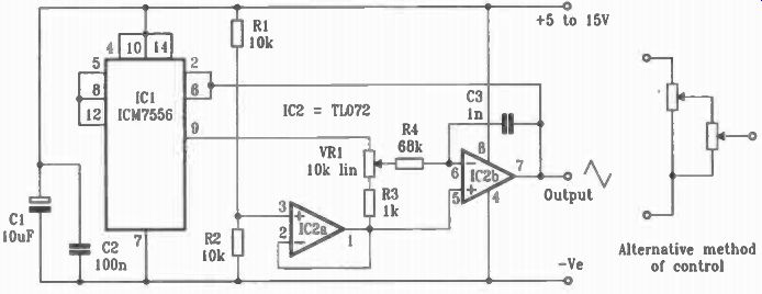
Fig.1.7 Variable Frequency Triangle-Wave Generator. Alternative method of
control.
Period and frequency calculations for the maximum frequency of this circuit are similar to those of the circuit of Figure 1.6. R3 sets the minimum frequency, in this case a tenth of the maximum. If R3 is omitted, the frequency control range will extend right down to zero. The maximum frequency, with VR1 the wiper of VR1 at the IC1 output end, can be calculated from:
f - 1.333 x R4 x C3 1
With the values shown the range is approximately 1-kHz to 10kHz and the output scale, using a "linear" component for VR1, is virtually linear.
Sometimes, some non-linearity of the control scale can be useful. The compression produced by linear control of period generally produces a scale which is far too cramped into one end to be of any practical use. Similarly, log-law variable resistors usually offer too much compression for most applications.
In any case, a feature of "log" variable resistors is that they don't usually have a smooth log law at all! Mostly they provide a slow change of resistance over the first part of their range followed by a much more rapid one over the rest. If this response is plotted as a graph it will often be found that it consists of just two straight lines with a sharp "knee" in the middle, showing that the track has been manufactured from just two types of resistive material. This is fine for volume control, but not very useful for accurate control of oscillator frequency.
Other types of variable resistor are made, inverse square law for example, but these are not often readily available to home constructors.
A scale compression technique that is sometimes useful is to replace VR1 with a dual-ganged linear type connected as shown to the right of the circuit in Figure 1.7. The wiper of the first section is connected to the top of the second, resulting in a control scale following something similar to a square law.
There are a couple of shortcomings with this; the "square law" isn't precise because the second pot represents loading to the first and the load on the voltage source to which they are connected also varies with their position, but provided these limitations are catered for this arrangement can provide a useful degree of scale compression. It can certainly be used with the oscillator of Figure 1.7. to provide finer adjustment at the low frequency end of the scale, while leaving the high end still reasonable controllable.
So far no "decoupling" capacitors have been shown in these circuits, as the majority have been so simple that they are likely to be used as part of other circuits- which will probably already have some decoupling . However, it is possible that some experimenters may wish to build this circuit as a useful signal source for the workbench, so suitable capacitors, C1 and C2, are shown. This is a very useful oscillator that has been employed by the author in a number of designs needing a reliable and easily controlled frequency source. It can operate from sub-audio to moderately high frequencies, well above 100kHz if required. The outputs available are the triangle wave from IC2b, square waves from IC1 pins 5 and 9, and as with the previous circuit the discharge transistor collectors are both avail able at IC1 pins 1 and 13.
Components for Figure 1.7
Resistors (all metal film, 0.6W)
R1 10k
R2 10k
R3 1k
R4 68k
VR1 10k linear pot, carbon
Capacitors
C1 10µF/25V electrolytic
C2 100nF ceramic
C3 1nF polyester or polystyrene
Semiconductors
IC1
IC2
ICM7556 dual timer, CMOS
TL072 dual JFET input op-amp.
Fig.1.7 Variable Frequency Triangle-Wave Generator.
Spot Frequency Function Generator
Figure 1.6 showed a circuit using an integrator with an ICM7556. The effect of the integrator, when supplied with a squarewave input from the timer, was to convert it into a tri angle wave. If the triangle-wave signal is applied to another integrator it will be modified further, this time into a sinewave.
This process can be used to generate a fairly pure sinewave of fixed frequency with a relatively simple circuit. The version shown here generates all three basic waveforms, square, tri angle and sine, at approximately equal peak-to-peak voltage amplitudes. With a nine-volt supply the amplitude of the sinewave, three volts peak-to-peak, is roughly equivalent to 1 volt RMS, a useful value for audio testing.
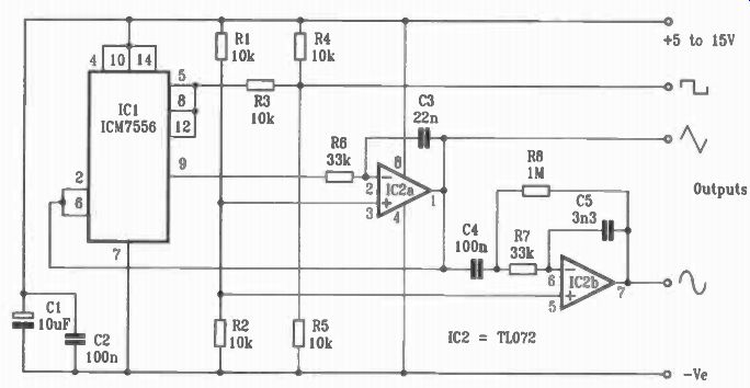
Figure 1.8
The circuit is shown in Figure 1.8. The dual timer IC1 and the integrator IC2a generate the square and triangle waves in the same manner as the earlier circuit, but with one small difference. An aim of this design was to generate all three outputs with roughly the same output voltage for use in rapid testing of the response of other circuits to the different waveforms. The triangle wave sets the initial value, with its peak-to-peak voltage of one-third of the supply. The squarewave initially has a value of the supply voltage as it swings from rail to rail, but it is then attenuated by the two resistors R4 and R5 to approximately the desired value. If it is not required these two resistors can be omitted.
The triangle wave is connected to the input of IC2b, a second integrator. Without some form of DC feedback the output of an integrator will eventually drift as far as it can towards one of the supply rails due to input offset voltages and currents, etc., so IC2b is AC coupled to the input signal through C4 and the high value feedback resistor, R8, maintains the correct DC output level. The values of these two component are high enough to avoid distortion of the signal at the operating frequency. The output amplitude is set by the values of R7 and C5 to the required level of about a third of the supply peak-to-peak. The frequency is calculated, as with the earlier circuit, from:
f = 1.333 x R6 x C5 1
A surprisingly good sinewave can be generated in this way, the only drawback being that the frequency cannot easily be adjusted. Any alteration of the input frequency to the second integrator will require adjustment of the values of R7 and C5 to maintain the correct sinewave output amplitude, and there is no simple way of doing this. Would that there were such a way! Most circuits capable of producing variable frequency sinewave outputs are fairly complex, but they will be covered later in this guide. Meanwhile there are many applications for which a fixed frequency sinewave signal source is useful, and this simple circuit should be sufficient for most of them.
Components for Figure 1.8
Resistors (all metal film, 0.6W)
R1 10k
R2 10k
R3 10k
R4 10k
R5 10k
R6 33k
R7 33k
R8 1M
Capacitors
C 1 C2 C3 C4 C5
Semiconductors
IC1
IC2
10pF/25V electrolytic
100nF ceramic
22nF polyester or polystyrene
100nF polyester or polystyrene
3n3 polyester or polystyrene
ICM7556 dual timer, CMOS
TI,072 dual JFET input op-amp.
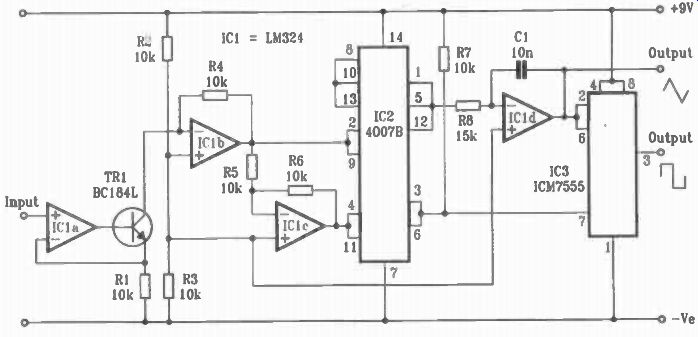
Fig.1.9 Voltage-controlled Oscillator with Equal Duty Cycle.
Voltage Controlled Oscillator With 50:50 Duty Cycle This, the last circuit of this section, is the most complex of the voltage-controlled oscillators to be shown in this section, incorporating some techniques that may prove useful to circuit designers in other applications. Unlike the circuits shown in Figures 1.4 and 1.5 which had pulse outputs, it provides both squarewave and triangle-wave outputs with 50:50 duty cycles.
This can be useful in many applications, especially in audio.
The frequency is controlled by a voltage which is referenced to the negative supply voltage.
The circuit is shown in Figure 1.9. The first two op-amps, IC1a and IC1b, act as a voltage level-shifter for converting an input that is referenced to the negative supply into one that is referenced to half the supply voltage. It works as follows. IC 1a biases the transistor TR 1 so that the control voltage, Vin, appears across the resistor R1. Nearly all the resulting current through this resistor reappears at the collector of TRI, so this part of the circuit is a voltage-controlled current sink. Negative feedback through R4 would normally cause IC2b to match the reference of half the supply from R2 and R3 at its inverting input, but it must also compensate for the current drawn from this point by TR1 so there is a corresponding voltage rise at its output. If R1 and R4 are equal in value this rise above half the supply will be equal to the value of the input voltage above the negative supply. If a control signal is already available referenced to half the supply this part of the circuit can be omitted, but often the control signal will be supplied with respect to negative and shifting the level can be something of a headache.
This arrangement does the job most efficiently.
The next op-amp, IC1c, is a straightforward unity-gain inverter. If the output of IC lb is, say, a volt above half-supply, the output of IC1c will be a volt below it. The outputs from these two op-amps are taken to IC2, a CMOS 4007B connected to form a 2-way electronic switch with poles at pins 2,9 and 4,11 and the common at pins 1, 5 and 12. Output from this point goes to the integrator formed with IC1d. Depending on the switch position, which is controlled by the level at pins 3 and 6, the integrator receives an input with polarity that is positive or negative of half supply, with a value dependant on the control ling input voltage but equal in both directions. The integrator output rate of change is therefore the same in both directions.
This goes to the input of the timer IC3, and the output of this controls the switch IC2, changeovers taking place as the input reaches one-third or two-thirds of the supply. In this circuit the "discharge" output has been used with the pull-up resistor R7 to control the switch so that the output of 1C3 remains free, but the output could be used instead, omitting this resistor.
The frequency of this circuit can be calculated from:
f - 2 xVxRxC E
Where E is the input voltage, V is a third of the supply voltage, and R and C are R8 and C1 in the integrator. With the values shown and a nine-volt supply the output is a little above 1 kHz per volt of control input. The output is linearly proportional to the control voltage, but of course will also change with supply voltage variations unless the input is a proportion of the supply.
The op-amps in the test circuit were the four contained in a single LM324 package. Using these, the circuit worked up to around 10kHz before distortion of the triangle-wave became pronounced. Replacing the integrator op-amp IC1d with a TL071 improved high frequency performance, and with a 100pF capacitor for C1 it then worked reasonably well to above 100kHz. At the other end of the range, it can run practically as slowly as the designer needs. Frequencies well below 1Hz are perfectly feasible. Op-amp IC1a must be a type that can operate with inputs and output at negative supply potential, and the input should not be more than about a quarter of the supply to allow sufficient working "headroom" for TRI. The squarewave output is available from pin 3 of IC3, and a triangle-wave output, with peak-to-peak amplitude of a third of the supply, can be taken from the output of IC id.
Components for Figure 1.9
Resistors (all metal film, 0.6W)
R1
R2
R3
R4
R5
R6
R7
R8
10k
10k
10k
10k
10k
10k
10k
15k
Capacitors
C 1
Semiconductors
IC1
IC2
IC3
TR 1
10n polyester or polystyrene
LM324 Quad op-amp.
CMOS, 4007B, dual complementary pair plus inverter.
ICM7555 timer, CMOS BC184L
Also see: