Basic CMOS R-C Oscillator
CMOS devices offer a lot of scope to designers of R-C oscillators. Circuits can be constructed both from basic gates and with ICs designed especially for use in oscillator circuits. With inputs that operate around half the supply voltage and outputs that can swing all the way to both positive and negative supply potentials, CMOS gates are ideally suited to stable oscillator design. Circuits using them are often simpler and more reliable than equivalent designs based on discrete devices such as transistors, and have largely replaced these in modern design. Their low power requirement and supply voltage range of 3 to 15 volts also makes them ideal for use in battery-powered circuits.
There are some pitfalls however, which should be understood and these will be fully explained in this section.
The basic requirement for most R-C oscillator circuits is a pair of inverters connected in series as shown in Figure 2.1.
Assuming that the input is to gate G1, both inverted and non inverted outputs are simultaneously available, from G1 and G2 respectively. The oscillator action is easy to follow. If it is assumed that the output from G1 is at the instant of going positive, the resulting positive input to G2 will cause the output of this to go negative and this negative signal will be passed through capacitor C1 and resistor RI back to the input of G1, accelerating the action until a complete change of state of both gates has taken place. The positive output from G1 will then commence charging C1, gradually raising the voltage at G1 input. When it reaches half the supply voltage G1's output will again begin to change state, this time to negative, and the whole cycle will repeat.
The time required for each half-cycle is 1.1 x R x C, so the frequency is given by:
f - 2.2 xRxC 1
where R is R2 and C is C1 in the circuit shown.
Suitable values for resistor R2 are from about 10k upwards, and for capacitor C1 from 100pF upwards. As the voltage polarity across C2 is reversed every half-cycle this component cannot be a polarised type such as an electrolytic, but most other types can be used. For good stability polystyrene and polyester capacitors are recommended.
Two outputs are available, one from each gate. Either or both can be used. They are opposite in phase, a feature which is often useful in circuit designs. As with the basic circuits of section 1 the frequency can be adjusted by using a variable resistor for R2, and the duty cycle can be altered by using combinations of diodes and resistors. Once again, it is the period that is controlled by this resistor, so the frequency control action will be non-linear.
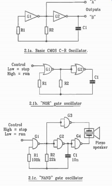
Fig. 2.1
Although it is simple and reliable, there are some potential pitfalls with this circuit which users should be aware of. Firstly, the output duty cycle is rarely quite even. For an exact 50:50 ratio or a very low frequency, see the next circuit in this section which uses a divider IC. Secondly, up to about 10kHz the output frequency generally conforms to the above formula but beyond this it becomes less predictable, usually being lower than calculations suggest. The frequency is also sensitive to supply voltage changes, generally increasing slightly as the voltage rises, and again this effect becomes more noticeable at high frequencies. CMOS gates are well-known for their low supply current requirements but this only applies when their inputs spend most of the time close to the supply rails. With intermediate input voltages their output stages can become partially conductive. Since the input to G1 changes relatively slowly, this gate draws current for part of each cycle. This is not usually a problem as with most gate types it involves only a few hundred microamps, but some of the high-current inverting buffers are not recommended for this type of circuit as they can draw sufficient current to overheat! Another effect of the slowly-rising input to G1 is instability and "glitches", or spikes, around the switching points. Often invisible unless viewed on a fast oscilloscope, this can produce unpredictable effects if the signal is used, for example, to drive a counter. This problem can often be cured simply by putting a 10k resistor in series with the drive to the counter. With the counter's input capacitance, this forms a low-pass filter which is usually sufficient to fix the problem. Another approach would be the use of "Schmitt" gates, such as those of the 4093B quad Schmitt NAND, but the hysteresis of these will affect the frequency calculations and also increase frequency shifts with variations in supply voltage.
The use of Schmitt gates does not cure the current consumption problem either.
These factors should not discourage designers from using this type of oscillator though, as it is simple, cheap and reliable and in most applications it operates without problems. So long as the potential pitfalls are understood, the cause of unexpected effects can usually be readily found and eliminated.
The purpose of resistor R1 is worth an explanation as it is not always understood. At the instant when the output of G2 starts to change state, let's say to positive, the side of capacitor C1 facing the input of G1 is at half the supply voltage. As G2's output switches, this side is raised initially to one and a half times the supply voltage. The same thing happens for negative output changes, only in the opposite direction with the input to G1 dropping to half the supply voltage below negative rail. Most B-series CMOS devices contain internal circuitry designed to protect their inputs from such voltages to prevent static discharge damage. This protection takes various forms depending on the manufacturer, but usually consists of diode networks arranged to conduct if voltages above or below the supplies are connected to them. In the R-C oscillator circuit this would result in rapid initial discharge of C1 whilst its voltage exceeded the supplies. This would adversely affect performance and stability so R1 restricts current flow into the protection, greatly reducing the effect. The value of this resistor should be reason ably high in comparison with R2, generally a ratio of four to one or greater is sufficient.
Although Figure 2.1a shows a circuit using two simple inverters, it can be built with NOR or NAND gates as shown in Figure 2.1b and 2.1c, which use gates from a 4001B and 4011B respectively. Surplus inputs can be connected together, or to positive supply, or they can be used as shown for controlling the oscillator. Where a four-gate IC is used the remaining gates can be used for a variety of purposes. Two oscillators could be built, one for audio frequency and the other operating at one or two hertz and gating the first to give a pulsed tone output. The spare gates could be used as buffers to prevent loading of the oscillator circuit. One useful suggestion is to use them for driving a piezo sounder device, using the two gates as buffers with opposite output polarities to create a "bridge" driver circuit. This is shown in Fig. 2.1c with G3 and G4 as the buffers.
Most of the inverting CMOS gates can be used in this type of oscillator. Some suitable types are shown in the following list:
4000B Dual 3-input NOR gate plus inverter
4001B Quad 2-input NOR gate
4002B Dual 4-input NOR gate
4011B Quad 2-input NAND gate
4012B Dual 4-input NAND gate
4023B Triple 3-input NAND gate
4025B Triple 3-input NOR gate
4093B Quad 2-input Schmitt NAND gate.
It is also possible to use the 4070B quad EX-OR and 4077B quad EX-NOR devices, since these 2-input gates can be used as inverters if one of the inputs is connected to the appropriate supply voltage. With the 4070B this is positive, for the 4077B it is negative. Again, this provides an option to control the oscillation with these inputs.
Components for Figure 2.1c
Resistors (metal film, 0.6W)
R1 100k
R2 22k
Capacitors
C1 10n polyester
Semiconductors
ICI 4011B CMOS quad NAND gate
Miscellaneous
Piezo sounder
CMOS 4060B 14-stage
Ripple Counter with Internal Oscillator
A useful version of the basic oscillator can be found in the 4060B oscillator and divider IC. This is essentially a 14-stage binary counter-divider, but unlike the other ripple counters, a pair of inverters already connected for use as an oscillator lurks behind pins 9, 10 and 11. This can be used in various ways, the most basic being as a C-R oscillator as shown at the top of Figure 2.2. All the previous information about this type of oscillator is relevant to this, including the operating frequency which is given by the formula
f = 1/(2.2 x R2 x C1).
R1 performs the same function as before and there are similar limitations on the maximum reliable frequency.
The input to the two gates, pin 11, is also internally connected to the "clock" input of the divider, giving some useful options. The output can be taken from any of the divider outputs. As they are multiples of complete oscillator cycles, all have perfect 50:50 duty cycles. They are buffered, so it is impossible to affect the oscillator frequency by loading them.
They can even be used for directly driving low-current LEDs, which is sometimes of value for constructing very cheap counting or timing circuits. The division process makes this IC especially suitable for the construction of very low frequency oscillators using sensible values of resistance and capacitance.
Sadly, the first three outputs are not available to the user. The first one externally available is output 4, at pin 7, which runs at 1/16th of the clock frequency. Even more of a disadvantage is the missing output 11, representing the clock divided by 2048.
This gap in the sequence of outputs is often a real nuisance as this IC would otherwise be ideal for very simple binary "address" generation.
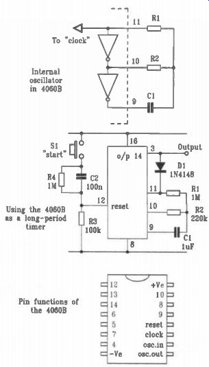
Fig. 2.2. 406013 Circuits -- Using the 4060B as a long-period timer Pin functions
of the 4060B
The "Reset" input, to pin 12, should be connected to negative supply for normal operation. If it is taken to the positive supply all the outputs will go low and remain there until the reset is returned to the low state and a clock input is applied. The oscillator outputs at pins 9 and 10 will also be low whilst the reset is active. This can be used to control the oscillator, or if the chip is being used to generate a binary output value, to reset this to zero and determine the starting time. Like all CMOS inputs, the reset pin should never be left unconnected as strange and unpredictable effects will result! Although not strictly an oscillator circuit, it's worth explaining how this IC can be used very effectively as a long-period timer, again with sensible values of resistance and capacitance.
For example, let's say a period of an hour is required. The timer circuit, made by modifying an oscillator with a single diode and a reset switch, is shown in the drawing. To initially set all the outputs to zero a positive pulse is needed at the reset input.
Connecting "reset" to ground through a resistor as shown allows it to be easily pulsed with positive by the push-button switch S1. C2 and R4 ensure that it gets only a single brief pulse when the button is pressed, so timing starts immediately even if it is not released promptly. The 14th output, from pin 3, is suitable for indicating completion of the required period.
Each complete cycle of this output takes 16,384 clock cycles.
However, it starts "low" and the time taken before it goes high represents half a cycle, or 8,192 clock cycles. This number of cycles per hour represents 2.28Hz, which from the formula requires a CxR product of 0.2 seconds. This is quite close to the 0.22 seconds that can be obtained from a 1pF capacitor with a 220k resistor, making these values a good starting point. I pF is readily available as a polyester component with a 5% tolerance, far more suitable for timing applications than the high value, wide-tolerance and leaky electrolytic that would be needed for a 555 timer providing this kind of interval. Whilst the output is low, diode D1 is reverse-biased. When it goes high, D1 conducts and "jams" the clock, stopping it until the reset is operated again. Whilst stopped in this way pin 10 will remain low, taking a current of a few microamps through R2 and R1 but this will be far less than even a CMOS 555's quiescent supply.
To check the circuit, output 4 from pin 7 can be viewed with a meter as it should be changing state roughly every 3.5 seconds. To set it up, output 8, from pin 14, can be used, as with the correct clock frequency this will change state every 56 seconds. Whilst such adjustments may be tedious, they represent a considerable improvement on circuits where the full hour has to be checked for each trial adjustment step.
The pin arrangement for the 4060B is also shown in Figure 2.2, where the numbers refer to the output stages.
Components for Figure 2.2
Resistors (metal film, 0.6W)
R1, 4 1M (2 off)
R2 220k
R3 100k
Capacitors
C1
C2
Semiconductors
D1
IC1
1uF polyester layer
100n polyester or ceramic
1N4148 silicon signal diode
4060B CMOS 14-stage counter with internal oscillator
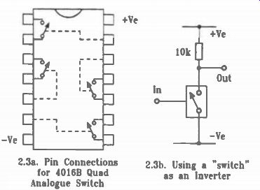
Fig. 2.3. 40168 Pin Connections and Use
CMOS 4016B Transmission Gate Oscillator
Another CMOS device that can be used to build a two-gate oscillator is the 4016B quad "analogue switch". This contains four electronic "switches", each of which can be "closed" by the application of a positive control voltage. If two of these are connected to form inverters, they can be used just like any other inverting gates to construct an oscillator. Figure 2.3a shows the pin connections for this IC. Note that, like other CMOS devices, unused inputs should be connected to either positive or negative supply, never left "floating". Figure 2.3b shows how a single switch can be arranged as an inverter. One side of the switch is connected to ground whilst the other is connected to the positive supply through a 10k resistor. Whilst the control input, labeled "in" in the drawing, is connected to a negative voltage the junction between the switch and resistor, labeled "out", is pulled up to positive by the resistor. When the input is supplied with a positive potential, the switch turns on and pulls the junction down to negative. Provided the resistor value is low enough in comparison with the load that the "gate" will be driving, the arrangement gives a performance similar to any other type of inverting gate.
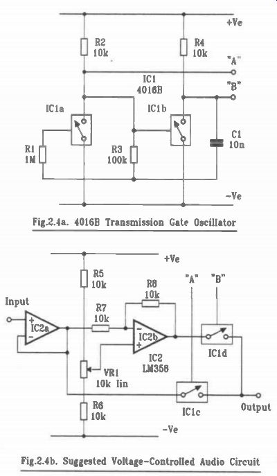
Fig.2.4a. 4016B Transmission Gate Oscillator
Fig.2.4b. Suggested Voltage-Controlled Audio Circuit
For use as an oscillator two of these "inverting gates" are built using two of the four switches of IC1, and the usual oscillator components are added as shown in Figure 2.4a. Two outputs are available, labeled "A" and "B". These, when viewed on an oscilloscope, are rather "messy", with glitches and instability around the switching points, and the frequency that can be achieved with this circuit is fairly low, though perfectly adequate for audio applications. A small disadvantage of the circuit is that one or other of the gates is always in the "on" state, so there will be a continuous drain on the supply current through the associated load resistor.
Like the others, the frequency of this circuit can be calculated from the formula f = 1/(2.2 x R x C). It departs from the calculated value more rapidly than most with increasing frequency, so calculation should be used only as a guide before practical testing when designing with it. To give some idea, the values shown should generate an output frequency of about 455Hz. In practice it ran at 430Hz, quite close to the calculated value. However, reducing the value of C1 to 100pF resulted in an output of only 24KHz, little more than half the calculated value. A 22pF capacitor connected across resistor R1 improved this to 39KHz so this may be worthwhile in some designs. The frequency of this circuit is fairly stable with changes in supply voltage and temperature and the duty-cycle of its output is reasonably close to a 50:50 ratio. As with most of the other two gate circuits, this can be altered by replacing R3 by diode and resistor networks.
This circuit is slow, requires two extra resistors and may draw more supply current. So why should anyone bother constructing an oscillator from the switches in this IC? Just one reason, but a good one. Like most of the of the other oscillators of this section it uses a single inexpensive IC, but this time the "gates left over" are two spare analogue switches, and with two opposite-phase outputs available for driving them these can be used in all sorts of ingenious ways, including as a two-way switch. When driven by the oscillator, they reject the glitches present around the changeover points to give clean operation, and in addition to digital levels they can control DC voltages and analogue signals. An sample application is shown in Figure 2.4b. Earlier circuits in this guide have shown ways of generating a signal with voltage-controlled amplitude by switching between the negative supply and a variable control voltage at the signal frequency. This is acceptable for many applications, but it results in an output which has an average DC value that changes with amplitude. In some circuits this causes problems.
One way to overcome it is to generate the inverse of the control voltage and switch between the two at the signal frequency.
This produces a signal which always has the same average DC level, no matter what the amplitude is. The circuit shown in Figure 2.4b uses a dual op-amp, with amplifier IC2a used as an input buffer to give the control signal a low source impedance, and the other amplifier, IC2b, operating as a unity-gain inverter to generate its complement. These two voltages are then connected to a "2-way switch" made with the remaining two 4016B switches IC1c and IC1d, so that an audio signal with varying amplitude but constant average DC value is available from its output. Most dual op-amps should be suitable for this simple circuit, although the one tested for this guide was the ubiquitous and cheap LM358.
Despite its simplicity this circuit has excellent performance and the uses are limited only by the designer's imagination. For starters, how about an output stage for detecting "null" in a DC bridge circuit? The pot VR1 shown in the circuit can be used to offset any quiescent voltage so that any change in the DC input, positive or negative, will be immediately audible. Since the ear has a logarithmic response a very large dynamic range will be covered, with excellent sensitivity at low levels.
Components for Figure 2.4
Resistors (all metal film, 0.6W)
R1 1M
R2, 4, 5, 6, 7, 8 10k (6 off)
R3 100k
VR1 10k linear pot, carbon.
Capacitors
C1 10n
Semiconductors
IC1 4016B CMOS quad analogue switch
IC2 LM358 dual op-amp.
CMOS 4047B Astable Oscillator
This is a little different to the preceding ICs in that it is purpose designed to be used as a versatile timer and oscillator. As such, it is capable of much better performance and higher frequencies. Whilst oscillators are often conjured up out of a few spare gates from ICs used in performing other circuit functions, when the designer wants to create an oscillator from scratch or needs improved performance this IC may be the best choice. Various pin connections allow it to be used in various configurations such as a monostable timer with positive or negative triggering, complementary outputs and reset, or as an astable oscillator with two output modes.
The pin functions for the 4047B are shown in Figure 2.5, with the basic connections for using it as an oscillator. This uses just one capacitor and one resistor to set the frequency, which as before is determined from the formula f = 1/(2.2 x R x C). R can have any value from 10k up to around 1M, whilst C should be greater than 100pF and must not be a polarised type.
Fig.2.5. 4047B Connections and Circuit -- Pin functions for the 4047B -- Astable
Oscillator Connections for the 4047B
Although the internal oscillator is still a two-gate circuit, the problem of the input protection diodes has been eliminated in this device so the usual series resistor to the input is unnecessary. This results in much better accuracy, especially at high frequencies.
When used as an oscillator three outputs are available. The first, "Osc out" is a buffered output operating at the basic oscillator frequency, available from pin 13. This is not guaranteed to have a perfect 50:50 duty cycle, but in practice it is generally much better than the simple two-gate circuits, especially at low frequencies. The other two outputs are "Q" and "Z1", from pins 10 and 11 respectively. These are provided from an internal single-stage divider circuit so they have perfect 50:50 duty cycles but run at half the primary oscillator frequency. They are buffered, and are complementary, so that whilst one is positive the other is negative. This has various uses, one of which could be driving a piezo sounder device placed across them to use them as a bridge output for greater volume. This works very well, producing quite a loud sound even from a 5-volt supply.
The connections for this are shown in Figure 2.5, for an output frequency of about 1.9kHz, a suitable frequency for most piezo sounders.
The oscillator frequency is given by:
f - 2.2 xRxC 1
but it should be remembered that only the output from pin 13 operates at this rate. The outputs from pins 10 and 11 run at half this frequency, so it can be calculated from:
f = 4.4 xRxC 1
The performance of this device is generally much better than either simple two-gate circuits or the internal oscillator of the 4060B. At high frequencies the output corresponds much more closely to the calculated value. A test circuit using 100pF and 22k, for an output of 206kHz, actually produced 173kHz with a supply of 10 volts, comparing very favorably with the 4060B which managed only 100kHz under the same conditions. Variation with supply voltage is less too, at 5 volts this circuit still managed to run at 155kHz. If a reasonably stable C R oscillator operating up to 100kHz is required, this IC is probably the best choice.
The "reset" input, pin 9, can be used to control the "Q" and "Q" outputs. Normally this input should be kept low, or negative. When connected to positive it forces "Q" low and "Q" high. It does not stop the oscillator however, this continues to operate and the signal from the "osc. out" pin 13 will still be present. If zero power consumption is required whilst the oscillator is not running, this is not the way to stop this one! Another way to stop it is to take pin 5, "astable", low. This does stop the oscillator, with "osc" and "Q" low and " - 0" high. This prevents the device from drawing any supply current at all, which may be necessary in some designs.
Components for Figure 2.5
Resistors
R1
Capacitors
C1
Semiconductors
IC1
Miscellaneous
Piezo sounder.
12k
10n
4047B CMOS, timer/oscillator.
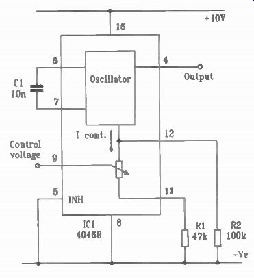
Fig. 2.6. 4046B Voltage-Controlled Oscillator
CMOS 4046B Voltage-Controlled Oscillator
A completely different type of oscillator circuit is to be found within the 4046B "phase-locked loop" IC. This versatile device has, amongst other things, a voltage-controlled oscillator that is exceptionally easy to use. Unfortunately descriptions of this are frequently difficult to follow, especially as it has two separate external frequency control connections. It is actually quite simple to work with, as this section will explain. However, there are some inherent problems with this !device that may exclude it from many designs and these will also be described in detail.
The basic connections for the oscillator are shown in Figure 2.6, which includes a greatly simplified version of its internal structure. The frequency is set by an external capacitor C1 connected between pins 6 and 7 and is controlled by a current, the value of which is set externally by the connections to pins 9, 11 and 12. The capacitor can have any value from 50pF upwards, but must not be a polarised type as the internal circuit operates by alternately grounding each end whilst charging the other to half the supply voltage. The component values shown are for an output frequency of about 2 to 61cHz.
There are two separate paths through which the circuit designer can set the oscillator control current, and it is not necessary to use them both. Usually the main one is through pin 11.
Control current flows from the oscillator to this pin through an internal voltage controlled resistor, whose value is set by an external control voltage applied to pin 9. Pin 11 is usually connected to ground through a resistor, shown in the drawing as R1. The control voltage can range from zero to the full supply potential. When it is zero, the value of the internal resistor is infinity so no current flows to pin 11, and if there is no connection to pin 12 the oscillator will stop. As the control voltage rises the internal resistor becomes more conductive, more current flows and the oscillator frequency rises. When the control voltage reaches positive supply the current from pin 11 is limited mainly by RI so this is usually referred to as the maximum frequency setting resistor. Current can also flow through a resistor from pin 12 to ground, shown as R2. This current is constant, regardless of the control voltage, and this resistor is often referred to as the minimum frequency setting resistor. However, as it produces a constant frequency increase right across the control range, it is easier to think of it as a positive frequency "offset". For instance, if the circuit was arranged to operate over the range 0 to 20kHz with R1 and C1, adding a resistor from pin 12 for a minimum of 51cHz will alter the range to 5 to 25kHz.
Once the current-operated nature of this oscillator is under stood, along with the two separate control current paths, it becomes simple to use. It provides a very simple way to control frequency with a voltage and the range covered can easily be 1000:1 or more, or it can be reduced to a tiny fraction by a suit able value of R2. The voltage control input has a very high impedance, so it can be used with high impedance signal sources without the need for buffering. The output has an excellent 50:50 duty cycle, and the maximum frequency can be set easily from sub-audio to 2 or 3MHz. The output frequency is reasonably linear with the control voltage, although there is some deviation below about 20% of the supply. It can also be stopped and started simply by pin 5, the "inhibit" input. This should normally be connected to negative but making it positive will stop the oscillator.
Unfortunately there is a downside with this IC as it has some significant problems relating to stability and variation between devices. These unfortunately exclude it from many applications for which it might at first sight appear ideal. By far the greatest problem is lack of stability with changes in supply voltage. For example, a trial circuit configured to run at 10kHz with a supply of 15 volts dropped to 6.8kHz at 10 volts and just 2.1kHz at 5 volts. This indicates that in practical use this IC will nearly always need a regulated supply voltage and performance is much reduced at 5 volts, limiting its usefulness in battery circuits. One possibility would be to regulate to 5 volts and then use an ICM7660 voltage doubler to give a stable 10 volt sup ply, but this would wipe out the benefits of simplicity and low cost. A random selection of six 4046B's tried in the same circuit yielded frequencies from 9.9kHz to 12.7kHz, suggesting that many applications would need pre-set or "select-on-test" adjustment for correct operation. There is also a slight sensitivity to temperature change, a burst of freezer spray causes a typical variation of around 2%. The wide variation of frequency with voltage makes it difficult to offer a formula for choosing R and C, but with a supply of 10 volts a reasonable starting point would be: 2 C x R followed by some practical testing to determine the exact values needed. This formula applies to both pins 11 and 12, in the case of pin 11 it assumes full positive supply voltage at pin 9. For half the supply voltage the frequency will be about half this value. The resistors from pins 11 and 12 to negative should be in the range of 10k to 1M. Although it is usual to operate this IC with a resistor from pin 11 as the main frequency-setting component, it is quite possible to leave this pin unconnected and use only a resistor from pin 12 to set a fixed frequency. It is then possible to use a much higher value resistor from pin 11 to ground to provide a very small voltage controlled range of adjustment. This is not always obvious in descriptions of this IC, but it is worth knowing because it could find some useful applications.
Components for Figure 2.6
Resistors (all metal film, 0.6W)
R1 47k
R2 100k
Capacitors
C1 10n polyester or polystyrene.
Semiconductors
IC 1 4046B CMOS "phase-locked loop".
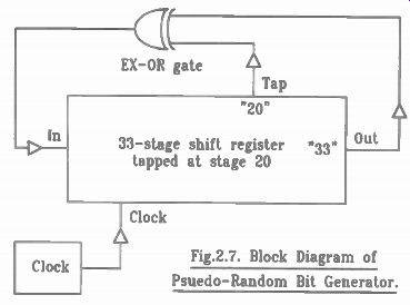
Fig.2.7. Block Diagram of Psuedo-Random Bit Generator.
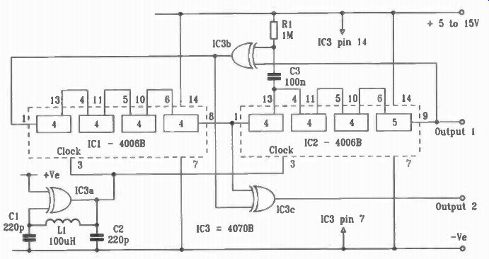
Fig.2.8. Pseudo-Random Noise Generator Circuit.
White Noise Generator
Considering that noise is a major problem in many areas of electronics, it comes as something of a surprise to discover that when some is needed, it is quite difficult to find a good source.
Zener diodes are widely regarded as being "noisy", but in practice most generate only microvolts. The base-emitter junction of a transistor, if reverse-biased into breakdown, will some times produce quite a lot of noise but the effect is unpredictable and therefore not suitable for use in reliable circuit designs.
Special "noise diodes" were once available, but the manufacture of these seems to have been discontinued for some time now. So, if a designer needs a good noise signal for testing or the creation of sound effects, how can it be generated?
One reliable source is the "Pseudo-Random Bit sequence" (PRBS) generator. This produces an apparently random stream of digital "1"s and "0"s, which simple filters can easily convert into an analogue noise source. Figure 2.7 shows a simplified block diagram of a PRBS circuit. It consists of a 33-stage shift register with a tap at stage 20. The signal from the tap is combined with the output in an EX-OR gate and returned to the input. The register is "clocked" by an oscillator at a fairly high frequency. Although the output is actually a repeating sequence, it is a very long one so the repetition is usually not a drawback. There are various combinations of register stage numbers and tap positions that give maximum sequence lengths, and for the length and tap shown the sequence is actually more than eight and a half thousand million bits long! Even with a 1.4MHz clock, it runs for almost two hours before repetition.
The full circuit of the noise generator is shown in Figure 2.8.
Two 4006B CMOS shift registers are used. These each contain four shift register "blocks", two with fixed lengths of four stages and two which can be either four or five stages long depending on the connections made by the user. These are connected in series to give the 33-stage overall length with a tap at stage 20 that is needed for this circuit. IC3b is one of the four EX-OR gates in a 4070B quad EX-OR IC. It is possible for a PRBS circuit to become "stuck" in a condition where the register stages contain nothing but "0"s, and since two "0"s on the inputs of IC3b will cause it to give an output of "0" the circuit will remain in this state until something happens to "kick-start" it. Unfortunately this often happens on start-up, so resistor R1 and capacitor C3 have been added to prevent it. If there is no positive output to C3 for a few milliseconds it charges through R1 to give a positive input to IC3b to set the sequence in motion.
The "clock" for the circuit is provided by another of the EX OR gates, IC3a, which is connected as an inverter for use with L1, C1 and C2 as an LC oscillator running at around 1.4MHz.
This type of oscillator will be covered in detail in a later section of this guide. Where a frequency above 100kHz is needed this is a more reliable source than an R-C circuit, and also requires only one gate. It will work with just about any inductor of the right value, the one used in the test circuit was a tiny wire-ended 100µH choke. These are physically very similar to resistors and are just as easy to use. The output of IC3a drives the clock inputs of both shift register ICs.
The output is taken from stage 33 of the register, pin 9 of IC2.
With some filtering, white noise is very useful for the creation of sound effects such as wind, surf, rushing water and so on, and in many instances these effects will be required in stereo.
The second output for this can be tapped if necessary with a third EX-OR gate, IC3c, which combines outputs taken from two other points in the circuit. Although the two outputs are obviously related, in practice they don't sound as if though they are and they can be used to create excellent stereo effects.
This circuit works well with supplies from 5 to 15 volts and draws very little supply current, so it is ideal for use with battery operated projects. The output amplitude depends, of course, directly on the supply voltage. If no other use is found for it, the inputs to the fourth EX-OR gate should be tied to positive or negative supply, not left floating. For most applications some filtering of the output of this circuit will be needed, so this will be covered next.
Components for Figure 2.8
Resistors
R1 1M (metal film, 0.6W)
Capacitors
C1, 2 220pF ceramic or polystyrene (2 off)
C3 100nF ceramic or polystyrene Inductor
L1 100µH miniature wire-ended choke.
Semiconductors
IC1, 2 4006B CMOS 18-stage serial-in, serial-out shift register (2 off)
IC3 4070B CMOS quad EX-OR
Filtering and "Pink Noise" Most applications for the PRBS white noise generator will need some filtering of its output. Figure 2.9 shows two filters that can be used. The simplest is a low-pass filter consisting of just a resistor and capacitor, as shown in Figure 2.9a, which will usually be sufficient. This attenuates the higher frequencies present in the signal above a "breakpoint" where the capacitive reactance is equal to the resistance. With the component values shown this is about 20kHz. It reduces the output level slightly, with a 10 volt supply the measured output is about 0.7V RMS. Larger values of capacitance can be used to give a "deeper" sound, like surf for instance. If the output level becomes too low it can be boosted with the op-amp circuit shown in Figure 2.9c, perhaps with some adjustment of the value of R2 to alter the gain. The voltage gain is given by:
G, = (R2 + R1)
R1
Some test applications need a source of "pink noise", and it has to be said that this also sounds quite pleasant. "Pink" noise requires slightly more complex filtering than the simple type shown in figure 2.9a as it has to attenuate the higher frequencies by only 3dB per octave instead of the 6dB per octave of the simpler circuit. The arrangement shown in Figure 2.9b gives a reasonably close approximation to pink noise, using a series of four "breakpoints". The output from this filter is rather low at just 40mV RMS, and it should also not be unduly loaded as this could affect the filtering characteristic. The simple amplifier circuit of Figure 2.9c will boost it back up to 400mV RMS and also buffer it, so that it can be connected directly to most loads.
The op-amp shown is a TL071 but for stereo applications the dual version of this, the TL072, could be used instead.
Components for Figure 2.9a
Resistors
R1 22k (metal film, 0.6W)
C1 330pF ceramic or polystyrene.
Components - Figure 2.91)
Resistors (all metal film, 0.6W)
R1 22k
R2 10k R3 3k3 R4 1k
R5 330 ohm
Capacitors (all 5% polyester layer)
C1 330n
C2 100n
C3 33n
C4 10n
Components for Figure 2.9c
Resistors (all metal film, 0.6W)
R1 4k7
R2 47k
Capacitors
C1, 2 10µF/25V electrolytic (2 off)
Semiconductors
IC1 TL071 op-amp.
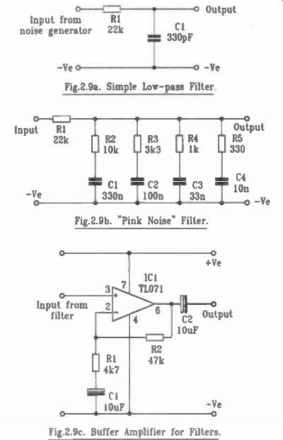
Fig.2.9a. Simple Low-pass Filter.
Fig.2.9b. "Pink Noise" Filter.
Fig.2.9c. Buffer Amplifier for Filters.
Fig. 2.9. Filtering for White Noise Generator.
Also see: