Audio Oscillator Construction
Following all the theoretical information, it seemed a good idea to end with a section on construction techniques using a practical example for readers to try out for themselves. Most of the circuits described can be constructed on 0.1" stripboard, which allows testing and experiments to be carried out with ease.
Stripboard is often used for prototype work because it permits immediate construction without the effort of designing and etching a printed circuit board, or the cost and delay of ordering and waiting for delivery should one be available ready-made. Results can be almost as neat and reliable as a PCB so many one-off designs never progress beyond stripboard construction. Many enthusiasts keep a permanent stock of the board ready for use whenever the need arises.
There are some disadvantages with stripboard construction.
With its breaks and links, and the care needed to ensure that components are correctly placed, it takes longer to construct than a printed circuit. The links, particularly on a board containing mostly logic ICs, can take up quite a lot of space as well as construction time. The paths taken by the circuit are often rather tortuous so, if a fault occurs, it can be troublesome to locate. This is compounded by the relative ease with which solder "bridges" can accidentally occur across tracks and tiny strips of copper can escape removal around the edges of "breaks". Compared with glass fiber PCB the material is rather fragile, so care is sometimes needed in handling and securing it. It is not suitable for 240 volt mains use, so any parts of the circuit using this or a similar high voltage will have to be constructed separately, and it is not always appreciated that there is quite a high capacitance between adjacent tracks, usually several picofarads, which may cause problems in high frequency circuits.
Some precautions need to be taken to avoid these potential problems, and the nature of the circuit to be built will have some bearing on these. Straightforward analogue circuits, where the signal follows a single linear path through the circuit, will normally cause no problems. More complex circuits may be easier to work with if constructed as a series of modules, or at least as separate areas on the board so that if a fault is pre sent, it will be simpler to locate. Digital circuits with multiple signal paths are perhaps better not constructed on stripboard.
They have a nasty habit of developing into "link farms" and can be very difficult indeed to trouble-shoot.
For all but the simplest circuits, it is advisable to draw up a layout on paper before commencing construction. A sheet of paper with a pattern of dots spaced at about 0.15" is very useful for drafting layouts, one of these can be made with a pen and then photocopied for future use. A fine-tipped (0.5mm) pencil and a pencil-style eraser then make drafting relatively easy. The sections of track actually forming the circuit can be indicated on this, making later trouble-shooting or modification easier. When drafting the layout, sensitive areas of track, those with high impedance, low signal levels or high frequencies, should be kept as short as possible to minimize the effects of leakage and stray capacitance. A useful trick with a very sensitive track is to connect those on each side of it to ground to form a simple "guard ring".
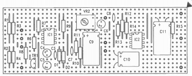
Fig.7.1. The Component Layout for the Wien Bridge Oscillator.
Finally, during construction, it is often a good idea to con struct the circuit a bit at a time if possible, testing each part as work progresses. The use of DEL sockets for ICs assists with this and allows the easy recovery of expensive components if the board is scrapped at some later time.
The Wien Bridge oscillator from Section 3 has been chosen as an example of layout and construction as it can be built as a relatively compact unit and will provide a useful test instrument for many constructors. The board should first be cut to size.
Although 16 strips of 44 holes are shown, constructors may wish to make it longer or wider to simplify fixing to a case or chassis. The underside with the breaks is shown in Figure 7.2.
Although breaks can be made by twiddling a twist drill between the fingers, a small inexpensive tool is available for the job and is well worth purchasing if regular use of stripboard is envisaged. As mentioned above, tiny strips of copper sometimes remain around the edges of breaks and can be difficult to see with the naked eye, so a check with a powerful magnifying glass is advisable before continuing.
The links should be fitted next. The position of these is shown with those of the other components in Figure 7.1. If appearance matters, and to many constructors it does, the links can make or break the job! Anyway, a neat board is more likely to be a reliable one. The way to make a really neat link with bare tinned copper wire is to take a piece of the wire and stretch it very slightly. This will make it absolutely straight, after which it can be cut into short pieces and the ends bent at right angles for insertion. The remaining components can then be fitted, generally in order of physical height to make life easy.
This means the resistors, followed by the small ceramic capacitors and the DIL sockets for the two ICs, the transistor TR1, the preset VR2 and finally the electrolytic capacitors. The three largest of these are placed horizontally so a spot of glue before insertion will help to secure them in position.
To simplify external connections to stripboard special pins are available. These are far more convenient than soldering wires directly to the board. They allow connections to be made from the component side, reduce stress on the copper strips themselves, and wires connected in this way are less likely to break off. The pins have to be pressed very firmly into place before soldering and, once again, an inexpensive hand tool is available to simplify the job.
Once the components have been inserted and soldered, it's worth checking the soldering with a magnifying glass because it's far easier to accidentally bridge a couple of stripboard tracks than it is with those of a PCB, and it's also harder to spot such bridges. Temporary connections should be made to the external components as shown in Figure 7.3 for testing, though it isn't necessary to wire all the capacitors to the switch, a single pair of them can be connected on their own. The two 15n components are recommended for this.
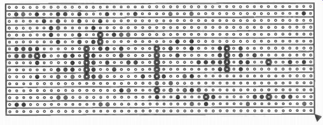
Fig.7.2. The Underside of the Wien Bridge Board.
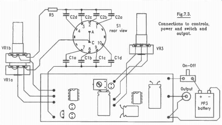
Fig.7.3.
Connections to controls, power and switch and output.
As the first stage of testing, the author usually recommends powering the board without the ICs, but with some means of checking the current drawn by the circuit. This will indicate any drastic problems such as short circuits without destroying expensive ICs and usually, if the current drawn by a published circuit is about the same as that taken by the prototype, there is a good chance the construction is OK. If this circuit is supplied with 9 volts, following a surge as the electrolytic capacitors charge, the current taken should be about 1.5mA. The next step is to fit IC1 and power the circuit again. This should raise the supply current to about 9rnA, and with VR1 at about half-travel it should be possible to measure the AC output from IC1a (pin 1) with a meter and set it to around 350mV RMS. If the circuit is OK the DC level measured at pins 1 and 7 of IC1 should both be at about half the supply voltage. If an oscilloscope is available, this can be used instead of a meter for checking and setting up the circuit.
Once the oscillator is working IC2 can be fitted and connections made to the level control VR3, which will raise the supply current to about 10.6mA. It's unlikely there will be any problems with this simple part of the circuit, so the final task is simply to set the maximum output level to 1 volt RMS, using the preset VR2 for this adjustment with VR3 set to maximum.
The project is completed by wiring the capacitors to the switch Si as shown in Figure 7.3, using the four unused tags on the switch as supports if necessary, and connecting this and the other controls to the board. Ribbon cable can be used to give a neat final appearance. None of the connections should need screening providing they are kept fairly short. A good method of construction is to secure everything to a metal panel which can then be "grounded" to the negative supply. This will minimize the effects of stray capacitance. As described in section 3, the power supply can be anything from 6 to 30 volts, so a 9 volt battery can be used, or a simple mains supply, perhaps with a 78L012 regulator to minimize hum.
Components for Figure 7.1
As given for Figures 3.4 and 3.5, plus:
2 x 8-pin DIL sockets
Case, knobs, socket, on-off switch, battery connector.
Squarewave Output for the Wien Bridge Project
An oscillator circuits of this type is often provided with a squarewave output in addition to the sinewave. Rich in harmonics, this can be used for a variety of tests, or it might be employed to synchronize another piece of equipment such as an oscilloscope to the test signal, often necessary when using the main signal at small amplitudes. "Squaring" of the signal is usually done by applying gain to the main signal until the amplifying device output is driven into saturation in both directions.
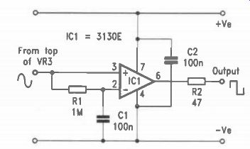
Fig. 7.4
The 3130E op-amp is particularly suitable for this as its output can swing all the way to both supply rails and its "slew rate", the speed with which its output voltage can change, is faster than many other types. Figure 7.4 shows a circuit using one of these devices. The input signal is taken from the top of the amplitude control VR3. It is connected directly to the non inverting input of IC1, and through the low-pass filter R1 and C1 to the inverting input. The filter ensures that only the average DC voltage of the input is applied to this input, not the signal itself. IC1 acts as a comparator, so when the direct input is above the average level its output is high, when it is below it the output is low. No frequency compensation is used with the op-amp in this circuit. Since it is not expected to behave in a linear fashion compensation is unnecessary and in fact would only slow down the output. The resistor R2 protects the output and ensures stability with capacitive loads. The local de coupling capacitor C2 is advisable to prevent spikes being introduced into the power supply.
This simple circuit provides a squarewave output with a good waveform all the way up to 100kHz and is more than adequate for use with the Wien Bridge project. It can be constructed as an add-on for the main board, or perhaps built on a small extension of it.
One small precaution that should be observed with this circuit is to keep the supply below 15 volts, as this is the maximum permitted for the 3130E device.
Components for Figure 7.4
Resistors (all metal film, 0.6W)
R1 1M R2 47
Capacitors
C1, 2
Semiconductors
IC1 100n ceramic (2 off)
3130E CMOS op-amp.
Also see: