Figure 11 Square wave output Q
| Home | Audio mag. | Stereo Review mag. | High Fidelity mag. | AE/AA mag. |
Circuit One
INVERTER or NOT GATE
This circuit (see Figure 5) is the simplest possible and uses only one gate of a 7400. Pins 1 and 2 are connected together and the circuit functions as an inverter, i.e. the output is the opposite of the input.
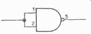
Figure 5.
If the input is 0, out is 1. If the input is 1 , output is 0.
As the circuit function is a negating one the gate is sometimes called a "NOT" gate. This expression is a better one. The term "inverter" is also used to mean a circuit using transistors or S.C.R.s to convert d.c. to a.c.
Circuit Two
AND GATE
As a NAND gate can be considered to be a "NOT AND" gate, if a "NOT" gate is placed after a NAND gate, the circuit becomes a "NOT-NOT-AND" gate. Two negatives make a positive (a principle common to mathematics and English grammar). The circuit is now an "AND" gate(see Figure 6).
To test a 7400 1.C., connect power supply to pins 14 and 7.
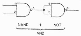
Figure 6.
Circuit Three OR GATE Placing a NOT gate in front of each input to a NAND gate produces an OR gate, see Figure 7. This is a 2 -input OR gate.
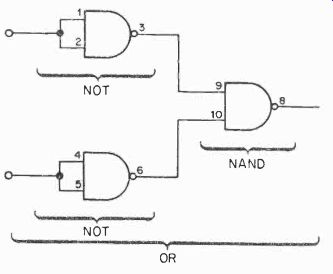
Figure 7
++++++++++++
Circuit Four
NOR GATE
In circuit (3) an OR gate was formed, a NOR gate is a NOT OR gate, by adding an additional NOT gate after an OR gate an NOR gate is formed (the above is for written use only!) (see Figure 8).
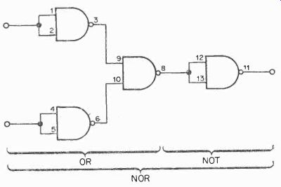
Figure 8.
++++++++
Circuit Five
LOGIC LEVEL INDICATOR
This circuit is based on the use of a 7400 NAND gate as an inverter or NOT gate to indicate logic levels. Two red LEDs (light emitting diodes) are used to indicate logic levels -
LED 1 and LED 2.
The longer lead of the LED is the cathode in most cases.
If the input is at logic level 1, LED 1 will glow. The output at pin 3 is the inverse of the input, i.e. 0 so LED 2 does not glow.
If the input is at logic level 0, LED 1 does not glow. The input to the inverter is 0, hence the output at pin 3 is 1 and LED 2 will glow.
The circuit function is input level 1, LED 1 glows; input level 0, LED 2 glows.
LED 1 should be marked 1. LED 2 should be marked 0.
The circuit can be powered from the logic circuit being tested (see Figure 9).
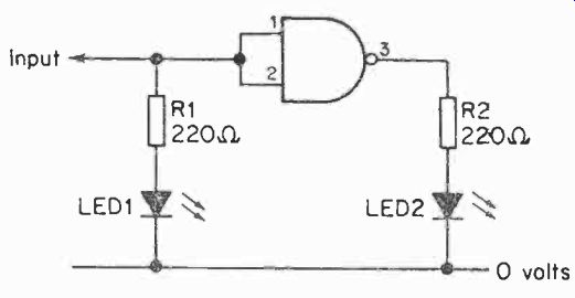
Figure 9
++++++++
Circuit Six
BISTABLE LATCH (S.R. FLIP-FLOP)
This circuit uses two NAND gates cross coupled to form a bistable latch circuit. The outputs are labeled Q and 0.
The bar over the Q indicates NOT. The two outputs Q and 0 are the complement of one another, i.e. if Q is at logic level 1,Q is 0; if Q is 0, Q is 1.
The circuit can be triggered into either of two stable states by a suitable input pulse. In effect this gives the circuit a "memory" and makes it a simple 1 bit (one binary digit) store. The two inputs are labeled S and R, Set and Reset, hence this circuit is also called a S.R.F.F. (Set Reset Flip - Flop).
This circuit is very useful and is employed in several circuits following (see Figure 10).
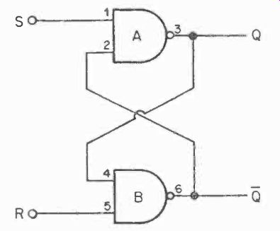
Figure 10
+++++++++++++
Circuit Seven
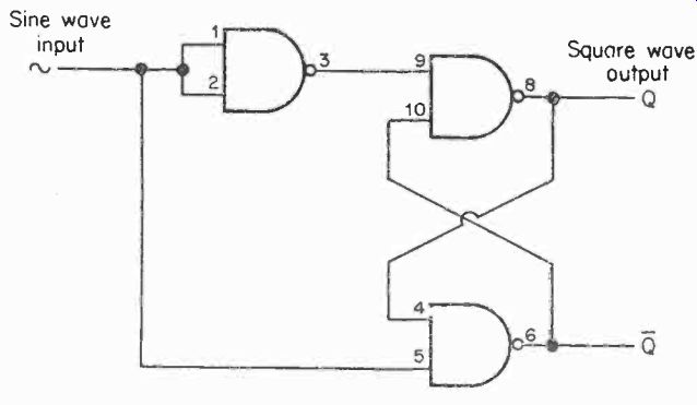
THE S-R FLIP-FLOP RECTANGULAR WAVE GENERATOR
The SR Flip -Flop circuit can be used as a generator of square waves. If the F.F. is triggered by a sine wave (which could be derived from the mains) of at least 2 volts P.P. the output is a square wave.
The square wave is very square due to the very fast rise and fall times of the circuit (examine output on an oscilloscope).
The inverter or NOT gate fed to the R input results in the inputs to the R and S inputs being complementary (see Figure 11).
Sine wave input ...
Figure 11 Square wave output Q
++++++++++
Circuit Eight
SWITCH CONTACT BOUNCE ELIMINATOR
This circuit uses a S-R FLIP-FLOP in a contact bounce eliminator. When switch contacts close the initial closure is followed by the contacts jumping rapidly several times between the closed and open position. This phenomenon can generate spurious pulses and cause erratic circuit operation.
In the circuit the first closure of the contacts latches the circuit, contact bounce does not affect the flip-flop. The switch shown is a single pole double throw type (S.P.D.T) (see Figure 12).
Figure 12
++++++++
Circuit Nine
MANUAL CLOCK
This is a variation on circuit eight. For experimenting with half adder and other logic circuits it is useful to be able to examine the circuit as it functions one pulse at a time. This can be accomplished by the use of a manual clock. Each time the switch is operated a single pulse will appear at the output. The circuit can be used with a binary counter each time the switch is operated one pulse (one only due to the anti -bounce effect of the circuit) will be generated and the count will advance by one (see Figure 13).
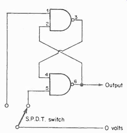
Figure 13
+++++++++++++
Circuit Ten
S-R FLIP-FLOP MEMORY
This circuit is developed from the simple S-R Flip -Flop.
The output depends on the previous input. D is the DATA input. An enabling pulse is required to trigger gates B and C. Q is the same logic level as D, i.e. it takes the value of D and remains in this state (see Figure 14).
The lead numbers are not shown to simplify the Figure, all five gates are 2 input NAND, two 7400s are required.
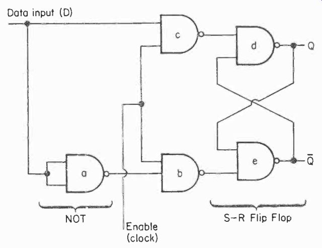
Figure 14 is a logic circuit only, but is readily translated into a circuit Figure. This simplifies Figures which have large numbers of logic gates involved. The enable signal can be a pulse from circuit nine.
The circuit operates in the presence of a "CLOCK" signal, a fundamental principle in computer operation.
Circuits nine and ten can be constructed from two 7400 I.C s and connected together.
+++++++++
Circuit Eleven
CLOCK CONTROLLED FLIP-FLOP
Circuit eleven is a variation on circuit ten. The date input is controlled by a clock signal, the output from the S-R Flip -
Flop is also controlled by the clock.
This Flip -Flop can be used in a storage register. The clock is a master controller of the flow of pulses in and out (see Figure 15).
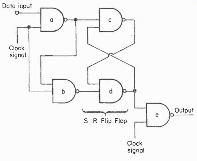
Figure 15
+++++++++++++++++
Circuit Twelve
HIGH SPEED PULSE INDICATOR AND DETECTOR
This circuit is developed from the S-R Flip-Flop and is used to detect and indicate a single pulse in a logic circuit.
A single pulse latches the circuit, the output is fed to the inverter and the red LED glows. The circuit will remain in this state until it is cleared by operating the S.P.S.T. reset switch. Test with circuit nine (see Figure 16).
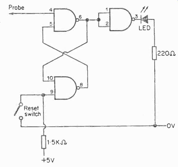
Figure 16
+++++++++++
Circuit Thirteen
"SNAP!" INDICATOR
This circuit is another use of the S-R Flip -Flop and uses two flip-flops. Seven gates are required. The basic principle in this circuit is the use of S-R flip-flops and INHIBIT lines.
S1 and ohm are switches which control the flip-flops. Once a flip-flop has latched the associated LED glows and the other flip-flop is inhibited from latching. If the switches are push button types - releasing the switch resets the circuit. The diodes used are 0A91 or any general purpose germanium diode (see Figure 17).
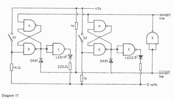
Figure 17
Gates A, B, C are the circuit for S1 and LED 1.
Gates D, E, F are the circuits for ohm and LED 2.
Gate G ensures that the INHIBIT and INHIBIT lines are complementary.
Many of the early transistor computers are now being broken up and the logic boards sold at low prices. Many of them used logic gates constructed from germanium diodes, these diodes are ideal for use instead of the 0A91.
+++++++++
Circuit Fourteen
LOW FREQUENCY AUDIO OSCILLATOR
The circuit uses two NAND gates connected as inverters and cross coupled to form an astable multivibrator. The frequency can be altered by increasing the value of CI and C2 (lower frequency) or decreasing the value of C1 and C2 (higher frequency). As electrolytic capacitors are used observe the polarity as shown in the Figure 18.
Figure 18.
Circuits fifteen, sixteen and seventeen are also examples of low frequency oscillators developed from circuit fourteen, but in these the output is used to make LEDs flash. Note the close similarity of the circuits.
If LEDs are connected up in this circuit they will flash but the flashing rate is so high that the eye cannot distinguish the individual flashes. This principle is used in pocket calculators.
++++++++++
Circuit Fifteen
TWIN LED FLASHER
This circuit uses two NAND gates to form a very low frequency oscillator, this drives two red LEDs and causes them to flash alternately. The circuit uses two NAND gates, the other two gates in a 7400 can also be used in a similar circuit but with different value capacitors to produce a different flashing rate.
If higher value electrolytic capacitors are used the LEDs will flash at a slower rate. Two suggested "novelty" projects using this circuit, are as follows.
If subminiature Tantalum electrolytics are used, the circuit can be very small. If three 7400s are used (12 LEDs) these together with a subminiature mains transformer and associated power supply can be encapsulated inside a cube of transparent plastic. The plastic encapsulation kits or "CLEAR CASTING" kits are available from most large toy and hobby stores.
The inner surfaces of the cube produce multiple images of the LEDs, if 12 red or orange LEDs are used and the cube is placed in a dark room the effect is of a cube of cold fire or flickering and pulsing light energy.
Another project suitable for a medical exhibit would be to build a hundred of the circuits (400 LEDs) and place the circuit in the interior of a model of the brain made from grey plastic. The LEDs should be fixed in the surface convolutions of the "brain". This example apart from electronics could be titled "THOUGHT".
Another idea is to place the circuit behind a painting or picture of a war scene, battle at sea, aircraft or tank battle.
Place the red or orange LEDs in the guns to simulate firing (see Figure 19).
Figure 19.
+++++++++
Circuit Six teen
FUSE TESTER
A simple development from circuit fifteen is a fuse tester working from a 7 1/2-volt or 9 -volt battery. LEDI indicates that the circuit is working. A green LED is best for this (and it also reduces the voltage applied to the I.C.).
LEDI indicates the circuit is operational when the TEST button is pressed. If LED2, a red LED, flashes this shows that the fuse is intact, if the fuse has blown, i.e. open circuit, the LED2 does not flash. This is a useful circuit because many fuses (e.g. the 1" types used on mains plugs) are made from a ceramic tube and it is not possible to see the use wire inside (see Figure 20).
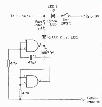
Figure 20.
+++++++
Circuit Seventeen
STROBOSCOPE
This circuit is developed from circuit fifteen and is a low power stroboscope. The circuit is really a high speed LED flasher. The red LED flashes but the eye is unable to resolve the individual flashes (persistence of vision).
The output is not very great so the stroboscope should be used in a darkened room. The gagged variable resistors alter the frequency of the flash so that the stroboscope can be used to give a stationary display. The resistors are described as 10 IC ohm + 10 MI gauged variable LIN (i.e. LINEAR TAPER), or 10 K ohm + 10 Ks2 stereo pot..- LIN (see Figure 21).
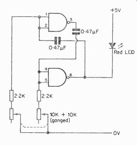
Figure 21.
The stroboscope can be used at a much higher frequency by changing the value of the timing capacitor. The LED is a light emitting diode and being a diode will work at a very high frequency. I suggest that it might be possible to take very high speed photographs using a LED strobe.
If anyone does wish to attempt this note that high speed infra -red sensitive film could be used with an infra -red emitting diode.
++++++++
Circuit Eighteen
LOW HYSTERESIS SCHMITT TRIGGER
Two NAND gates function as a Schmitt trigger in this circuit.
The diode is a high speed silicon type 1N4148 or 1N914.
For these who wish to experiment with the circuit, the hysteresis is determined by RI (see Figure 22).
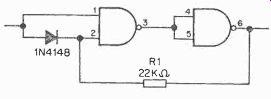
Figure 22.
+++++++++++++++++++++
Circuit Nineteen
FUNDAMENTAL FREQUENCY CRYSTAL OSCILLATOR
This is a crystal controlled oscillator. Two gates are connected as inverters, the resistors bias the gates into the correct operating point. The third gate is connected as a "buffer" to avoid loading the oscillator.
Note that when a crystal is used in this circuit, it will oscillate at its fundamental frequency, i.e. NOT at a harmonic or overtone frequency. If the circuit works at a frequency much lower than expected, this means that the crystal frequency marked is an overtone, i.e.
a multiple of the fundamental frequency (see Figure 23).
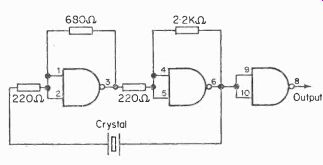
Figure 23.
++++++++++++
Circuit Twenty
TWO BIT DECODER
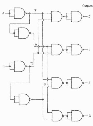
Figure 24.
This is a simple two bit decoder. The inputs are along lines A and B, outputs are along lines 0, 1, 2, 3.
A can be 0 or 1.
B can be 0 or 1.
If A and B are at 1, this is a binary count of 11 equal to denary 3 and the output along line 3 is "high". Similarly, A, 0 B, 0 output line 0. Maximum count depends on the number of inputs, maximum counter with two inputs is 22 - 1 = 3. The circuit can be expanded, e.g. if four inputs are used A, B, C and D, maximum count is 24 - 1 = 15 and the outputs are from 0 to 15.
Note on the circuit the use of NOT gates. Some lines are B, some B (not B), note the inversion of B to B and later inversion of B back to B on some lines.
This is a simple circuit but it requires 3 x 7400 I.C.s (12 gates) and the interconnections are becoming complicated.
The transistor and I.C. produced revolutions in electronics, but it may not be appreciated that a development of almost equal importance was the printed circuit. The inter connections on a printed circuit may be very difficult to work out for the "Master" board design, but once this has been tested and proved the circuit board. containing all the connections, can be reproduced photographically thousands or millions of times (see Figure 24).
+++++++++++++++
Circuit Twenty-One
TWO BIT DECODER (SIMPLIFIED) The two bit decoder of circuit twenty required 12 gates, three 7400 I.C.s. It can be seen that the circuit simplifies to four NOT gates and four AND gates. A simpler version can be used by employing the special purpose inverter and, AND gate I.C.s.
The 7404 contains six NOT gates or inverters and the 7408 contains four 2 -input AND gates. By using a 7404 and 7408 only two I.C.s are required and two gates of the 7404 are spare.
On the 7404 and 7408 pins 7 are 0 volt and pins 14 + 5V (as with the 7400) (see Figure 25).
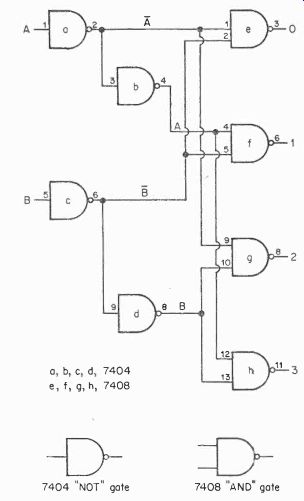
Figure 25
++++++++++++
Circuit Twenty -Two
PHOTO SENSITIVE LATCHING CIRCUIT
This is a simple photoelectric circuit using two NAND gates to form a circuit with latching action. The transistor used is a general purpose audio NPN silicon type such as the BC108, the lead connections are shown on Figure 26. The photo sensitive element is a Cds (Cadmium Sulphide) photo conductive cell. The CdS cell is in effect a resistor whose resistance varies in accordance with the light shining on it.
In complete darkness the resistance may be 10 M ohm (10 million Ohms) and in comparison directly under a bright electric light the resistance may drop to 100ohm.
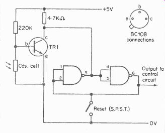
Figure 26.
The circuit operation is as follows. The Cds cell is normally illuminated by a small torch bulb, and the resistance of the cell will be very low, grounding the base of TR1. As the base is grounded Tr1 does not conduct hence there is no voltage drop across the 4.7 ohm resistor in the collector circuit, so that the voltage at the collector is high. If the light is blocked off the resistance of the Cds cell rises (not instantaneously - there is a slight delay in the resistance change of a Cds cell - not important in this circuit). Tr1 conducts, there is a voltage drop across the 4.7 Kohm resistor and the voltage at the collector falls. This fall in voltage triggers the latch. The latch has to be reset by momentarily depressing the switch.
++++++++++++++
Circuit Twenty Three
TWIN TONE AUDIO OSCILLATOR
This is a two tone oscillator using four NAND gates. The circuit consists of two oscillators, a high frequency oscillator (0.22 µF capacitors) and a low frequency oscillator .(47 uF capacitors). The oscillators are connected together in such a way that the high frequency is modulated by the low frequency. The circuit gives a warbling output which is much pleasanter than the single tone produced by a 2 -gate oscillator (see Figure 27).
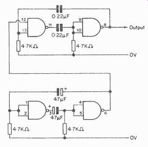
Figure 27.
++++++++++++++
Circuit Twenty -Four
CRYSTAL CLOCK OSCILLATOR
This is a crystal oscillator for use with a L.S.I. I.C. clock "chip" and provides a 50 Hz reference when used with an I.C. frequency divider chain.
The output is at 500 kHz and should be connected to four 7490 I.C.s in cascade. Each 7490 divides by 10 giving a total division of 10,000, the output is then 50 hz (500,000 10 ÷ 10 ÷ 10+ 10 = 50).
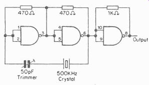
Figure 28
The 50 Hz reference is usually derived from the mains but a clock I.C. can be inaccurate if the mains is unstable due to waveform distortion which can occur if thyristor equipment is used on the same phase of the mains (next door for example).
Drill controllers, power controllers, light dimmers and some colour televisions use thyristor circuits which can disturb the mains. If you have an electronic clock which behaves erratically, this is the most probable cause.
The 50 pF trimmer is adjusted so that the crystal frequency is exactly 500 kHz (see Figure 28).
+++++++++++++++++
Circuit Twenty –Five
SWITCHED OSCILLATOR
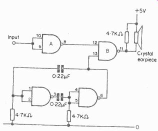
Figure 29.
This circuit consists of a tone generator and an electronic switch. The tone generator runs continuously but there is no output from the earpiece until there is a logic 0 input to gate A. A logic 0 input at gate A is inverted to a logic 1. The logic 1 opens gate B and the audio tone is fed to the earpiece.
Although a small crystal earpiece is used this produces quite a loud sound. The circuit could be used as a buzzer with an electronic alarm clock I.C. (see Figure 29).
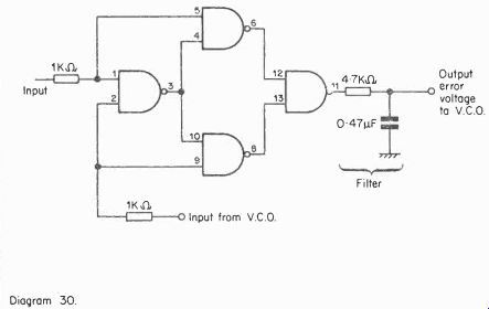
Figure 30
+++++++++
Circuit Twenty–Six
PHASE DETECTOR
This is a phase detector which uses four NAND gates. The phase detector compares two inputs and produces an error voltage in proportion to the difference between the two frequencies used as inputs. The output from the detector is followed by the 4.7 K&2 resistor and the 0.47 AF capacitor to give a d.c. error voltage (see Figure 30).
The phase detector can be used in a P.L.L. (phase lock loop) system and Figure 31 is a block Figure of a complete P.L.L.
system. The error voltage produced by the phase detector is amplified and controls the frequency of a multivibrator V.C.O. (voltage controlled oscillator).
The P.L.L. is a very useful system and can be used for F.M demodulation at 10.7 Mhz (radio) or 6 MHz (TV sound) or to regenerate the 38 KHz subcarrier in a stereo multiplex decoder.
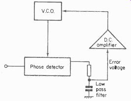
Figure 31. Phase lock loop system.
+++++++++++++++++
Circuit Twenty-Seven
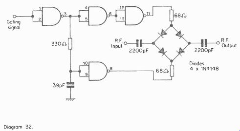
Figure 32
controls the diode bridge. The diode bridge conducts to allow the passage of RF or does not conduct to block the passage of RF. The amount of RF allowed through is a function of the gating signal.
The diodes are high speed silicon diodes type 1N4148 (see Figure 32).
++++++++++++++++
Circuit Twenty–Eight
REFERENCE FREQUENCY SWITCH
The circuit uses five NAND gates to form a 2-frequency switch. A bistable latch circuit is used with a S.P.D.T. switch to eliminate contact bounce (see Figure 33).
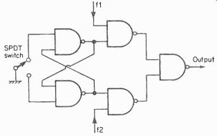
Figure 33. Input frequencies f1 and f2.
The output from the fifth gate is either f1 or f2 depending on the switch position used.
++++++++++++++++++
Circuit Twenty -Nine
SWITCH CONTACT BOUNCE ELIMINATOR
Most switches especially low cost types display some degree of "contact bounce". This is of no consequence in most electronic circuits, but if such a switch is used in a logic circuit, operation of the switch may produce spurious pulses.
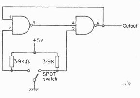
Figure 34.
The circuit uses two NAND gates (see Figure 34). This application can also be used as a single pulse generator for use with testing or demonstrating flip-flops or other logic circuits.
++++++++++
Circuit Thirty
TWO BIT DATA CHECK
This is another simple "computer type" circuit which can be used to demonstrate logic functions. Spurious pulses can occur in a computer causing errors. Error checking is done by adding an extra bit (binary digit) in "words" so that the total number of is in a computer "word" is always odd or always even.
This system is described as a "PARITY CHECK". The circuit checks odd or even parity for two bits. Note the similarity to the phase detector circuit.
This demonstrates how other applications can be devised by slightly altering the function of a "computer -type" circuit (see Figure 35).
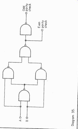
Figure 35
+++++++++++++
Circuit Thirty-One
BINARY HALF ADDER CIRCUIT
This circuit uses seven NAND gates to form a half adder circuit (see Figure 36).
A0, B0 are the binary digit inputs. S0, C0 are the sum and carry lines.
In order to understand how these circuits work think how simple arithmetic is taught to children. Refer to the half adder TRUTH Table - Figure 37.
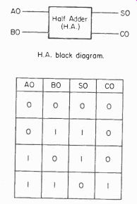
Figure 37. Half Adder truth table.
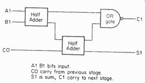
Figure 38. Full adder block Figure.
Consider the Truth Table in terms of binary arithmetic:
0 and 0 is 0 I and 0 is I sum 1 carry 0.
0 and 1 is I sum 1 carry 0.
1 and 1 is 10 sum 0 carry 1.
10 is not "ten" but is pronounced as "one zero" and represents 1 x 2' + (0 x 2°).
Two complete half adder circuits plus an "OR" gate form a full adder circuit - see Figure 38.
On Figure 38, A1 and B1 are the binary digits, C0 is the carry from the previous stage, SI is the sum, C1 is the carry to the next stage.
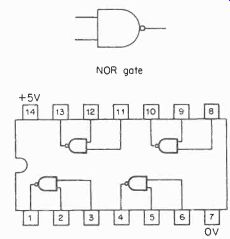
Figure 39.
7402 I.C. connection details.
(Quad 2 input NOR).
+++++++++++++++
Circuit Thirty –Two
NOR GATE HALF ADDER
This circuit and circuit thirty-three are based on the use of NOR gates. The 7402 I.C. contains four 2 -input NOR gates.
See Figure 39 for connection details of 7402: pin 7 = 0V; pin 14 = +5V as with the 7400 I.C.
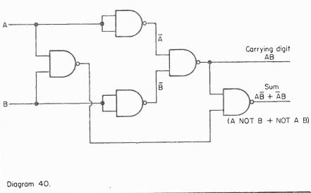
Figure 40
The half adder uses five NOR gates - see Figure 40.
Compare circuit thirty-two with circuit thirty-one which uses seven NAND gates. Output lines:
sum = AB + AB (NOTA.B + A.NOTB) carry = A.B
+++++++++++++++++++
Circuit Thirty -Three
NOR GATE FULL ADDER
This is a full adder circuit which uses two NOR gate half adders plus two additional NOR gates.
The circuit uses a total of twelve NOR gates and will require three 7402 I.C.s (see Figure 41).
The output lines are:
AB + K(AB + AB) = (sum) and (AB + AB)K + (AB + AB)K = (carry).
Input lines A, B and K.
K is the carrying digit from the previous column.
Note that the output is via two NOR gates which are equivalent to an OR gate. The circuit resolves again to two half adders plus an OR gate. Compare with previous circuits.
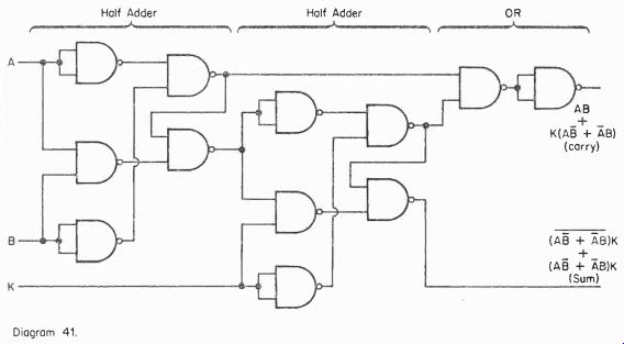
Figure 41
+++++++++++++++++++
Circuit Thirty–Four
SIMPLE SIGNAL INJECTOR
A simple signal injector for checking the output stages of transistor radios etc. can be made using two NAND gates.
The circuit can be powered by three 11/2 volt batteries in series (see Figure 42).
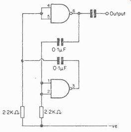
Figure 42
+++++++++++++++++++
Circuit Thirty-Five
SIMPLE AMPLIFIER
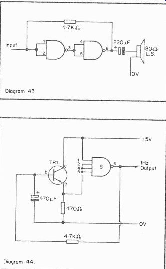
Figure 43
Two NAND gates connected as inverters can be connected in series to form a simple audio amplifier. The 4.7 Ks2 resistor produces negative feedback in the circuit, but the distortion is still high. The amplifier will drive a 25 to 80 ohm impedance loudspeaker directly. An 8-ohm loudspeaker can be connected but the I.C. may get very warm in use due to the extra power dissipated.
A lower value of resistor, e.g. 2.2 K2 can be used for better results, but lower volume (see Figure 43).
Figure 43
+++++++++
Circuit Thirty -Six
LOW SPEED CLOCK
This circuit uses a Schmitt trigger in a low frequency oscillator when the RC values are as shown. The clock frequency is about 1 1-lz, i.e. 1 pulse per second. The low speed clock is useful for demonstrating the action of circuits "in slow motion". TR I is a general purpose NPN transistor such as the BC108 (see Figure 44, above).
7413 pin 7 = 0V. Pin 14 + 5V.
The 7413 is a dual Schmitt trigger. The corresponding pins for the second trigger are 13 (1), 12 (2), 10 (4), 9 (5) and 8 (6).
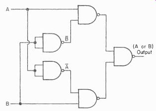
Figure 45.
++++++++++
Circuit Thirty -Seven
EXCLUSIVE OR GATE
The circuit is for an "exclusive" OR gate, using five NAND gates. The difference between an exclusive OR gate (XOR) gate and a normal OR gate is that for an output of I the inputs can be A = 1, B = 1 or A and B = 1, but the XOR inputs are A = 1 or B = 1 wily. See the two truth tables for OR and XOR gates (Figure 46). The circuit Figure for the XOR gate is Figure 45.
Note the use of inverters for cross coupling.
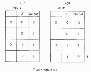
Figure 46. Truth tables.
++++++++++++++++
Circuit Thirty-Eight
DIVIDE BY SIX 7490 CIRCUIT
The 7490 is a useful ÷ 10 frequency divider for use at frequencies up to a few MHz (see Figure 47). It can be considered as a ÷ 2 and ÷ 5 circuit usually connected in cascade ÷ 2 then ÷ 5 to give the ÷ 10 function. However by altering the connections between the connecting pins from the normal arrangement, the 7490 can be used to divide by 2, 3, 4, 5, 6, 7, 8, 9 or 10, by setting the point at which the internal counter resets to zero. When used as a ÷ 10 counter it is connected so that the circuit counts up to 10 and then returns to zero.
The example used in this circuit is six, the counter is set to stop counting at 1010 and then return to 0000, 1010 is the binary equivalent of 6.
This mode of operation is very useful for electronic clock circuits with a 50 Hz reference input:
divide by 5 then 10 = 1 pulse per second;
divide by 6 then 10 = 1 pulse per minute;
divide by 6 then 10 = 1 pulse per hour;
divide by 6 then 4 = 1 pulse per day.
(An electronic clock is a good classroom project. Of course complete clock circuits are available in one I.C., but an electronic clock can be divided into a number of sub-circuits each to be completed by one pupil or pair, e.g.
sections above:
(i) ÷ 50 circuit (ii) ÷ 60 circuit (iii) ÷ 60 circuit (iv) ÷ 24 circuit (v) power supply (vi) display (vii) 50 Hz reference pulse shaping circuit.)
Note that the power supply connections to the 7490 are different: pin 5 is 5V+; pin 10 is 0V (see Figure 47).
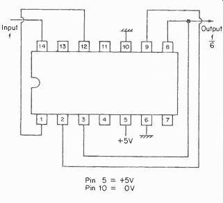
Figure 47.
7490 I.C.
The 7490 contains four counter stages: Q1, Q2, Q3 and Q4
Outputs are:
Q1 12 2° Q2 9 2' Q3 8 22 Q4 11 13
The counter also has four control pins: 2 and 3 reset to 0;
6 and 7 reset to 9. The circuit is connected so that a pulse from Q2 and Q3 resets the counter, i.e. when the state of count is :
Q4 Q3 Q2 Q1 , to zero.
0 1 1 0
++++++++++++++++++++
Circuit Thirty–Nine
74121 PULSE GENERATOR
This is a circuit using a 74121 monostable circuit as a single high speed pulse generator. Each time the button is pressed a single pulse of 0.5 µsec (half a microsecond) duration is generated.
The pulse length depends on the values of R and C connected to pins 10 and 11 (C) and 9 (R).
Pulse duration ^ 0.7 CR, where C is in Farads, R is in ohms.
In this case:
C = 330 pF R = 2.2 K ohm.
Converting units to ohms and Farads:
C = 330 x 10-'2 F R =2.2 x 10^3E2.
T =1330 x 10-12 x 2.2 x 10^3 x 0.7 seconds. If we multiply by 10^6 this gives the answer in micro-seconds.
T .0-- 330 x 10^-12 x 2.2 x 10^3 x 10^6 x 0.7.
T 330 x 2.2 x 10^-3 x 0.7.
T -=" 0.5082.
The time is approximately only, resistors have a tolerance of 5%, capacitors 10% or more.
The time can easily be altered by using different values of C, e.g. if a 0.680 pF capacitor is used the time duration is about 1 microsecond or 1 /sec (see Figure 48).
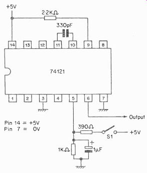
Figure 48
++++++++++++++++++++
Circuit Forty
LOGIC SWITCH
This circuit is identical in action to a S.P.D.T. switch but here the switching is electronic and not mechanical and can work at very high speed. C is the control signal.
The output is A if C = 0, output is B if C = 1 (see Figure 49).
A, B inputs, C control signal.
B 0 Equivalent switch.
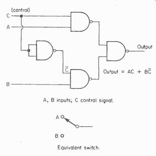
Figure 49.
Four NAND gates are used. C controls the gating of A, where as an inverter gives the complement C (not C) to control B so that the output can be labeled:
AC +BC.
The small Figure shows the equivalent mechanical switch. In fact the direct mechanical equivalent would be a relay, where a control voltage operated the relay which switched between A and B.
++++++++++++++
Circuit Forty-One
BINARY DISPLAY
Here a 7490 is used to count the 1 Hz pulses from a slow clock (e.g. circuit thirty-six), the four LEDs are illuminated via the flip-flops in the 7490 and flash on and off in a binary sequence. Four red LEDs should be used, red LEDs have the greatest light output for a given diode current (see Figure 50).
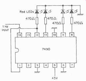
Figure 50
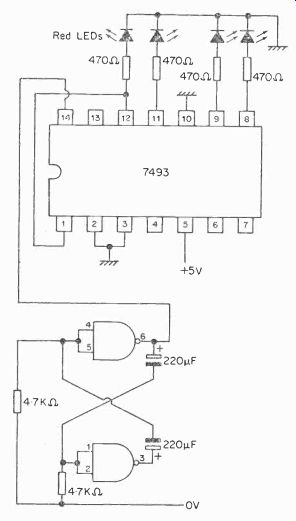
Figure 51.
+++++++++++++++++++++
Circuit Forty -Two BINARY COUNTER
Circuit forty-two is similar to circuit forty-one, but uses a 7493 4 -bit binary counter, and two NAND gates of a 7400 as a very low frequency oscillator. 7493 pin 5 is +5V and pin 10 is 0 (see Figure 51).
+++++++++++++++++++++
Circuit Forty -Three SIGNAL INJECTOR
This signal injector uses half a 7413 I.C. The circuit uses a Schmitt trigger as a multivibrator (see Figure 52).
Figure 52
+++++++++++++++++++++
Circuit Forty–Four
1 MICROSECOND DELAY CIRCUIT
The circuit uses a 74121 monostable (refer to circuit thirty nine) as a 1 u-sec delay circuit. The 74121 is set to produce a pulse width of 1 u-sec. The output pulse is differentiated to give 2 pulses, one at the beginning, one at the end of the 1 u-sec period.
If a negative pulse triggers the monostable another negative pulse will appear at the differentiator output 1 µsec later.
The 1N4148 high speed diode blocks off the positive pulse (see Figure 53).
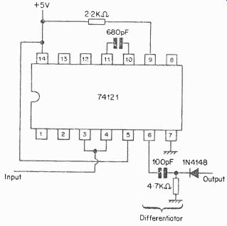
Figure 53.
++++++++++++
Circuit Forty -Five
SIMPLE 5V POWER SUPPLY AND 50 Hz SQUARE WAVE GENERATOR
This is a simple 5V power supply which can power 2 or 3 I.C.s and also includes a 50 Hz square wave generator.
The square wave generator uses a Schmitt trigger (IC. 7413) to produce square waves from a 50 1Iz sine wave input. A small 9-0-9V 100mA mains transformer is employed.
The 2N697 transistor should be fitted with a T05 heat sink (see Figure 54). The rectifiers are silicon 50 piv type 1N4001.
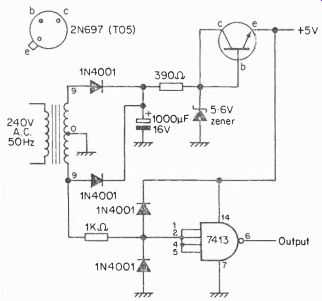
Figure 54
++++++++++++
Circuit Forty–Six
LOGICAL PUZZLE
There is an old puzzle concerning a prisoner, two guards and two doors. One door leads to freedom, the other door leads to death. One guard always tells the truth, the other guard always lies. The prisoner is allowed to ask one question of one of the guards and must then proceed through one of the doors. What is the question? Looking closely at the question we can see several binary situations. One of two doors, life or death, truth or lie.
The problem can be represented as a series of logic gates.
The doors can be labeled 1 and 0. The guard who lies can be a "NOT" gate and the guard who tells the truth can be Input 1 or 0 Input 1 or 0 Liar Truth-teller Ea° (a) Truth-teller (b)
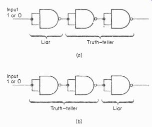
Figure 55.
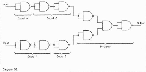
Figure 56.
2 "NOT" gates in series, i.e. someone who does NOT, NOT tell the truth.
The breakthrough in the problem is to realize that the information must involve both guards, i.e. ask one guard what the other one would say. Represent this by Figure 55(a) and 55(b): The information is either 1 or 0. Hone guard is asked "What would the other guard say if asked which is the door to freedom?", the situation is either 55a or 55b. The prisoner does not know which but in a or b the logic process is the same.
An inversion takes place, the answer given to the prisoner is the opposite of the correct one. Hence if the prisoner functions as a NOT gate, he takes the opposite of the given answer, and this is the number of the door to freedom.
A circuit to indicate either situation requires an OR gate as the answer is NOT the one given by the guard a NOR gate is used.
Figure 56 represents both situations, the input represents the number of the door.
++++++++++++++++
Circuit Forty–Seven
HALF ADDER DESIGN
A greater understanding of the function of a half adder circuit may be obtained by examining the Truth table for the addition of two binary numbers - see Truth table Figure 57.
Note that in the dotted box the A, B inputs and the sum are identical to the function of a NAND gate.
Examine the Truth table again, more closely; see Figure 58.
The function inside the dotted box is identical to the exclusive OR (XOR) function and the carry table is almost the inverse of the sum, so that the function is almost XOR + NOT (for the carry table). The half adder is XOR + NOT except when
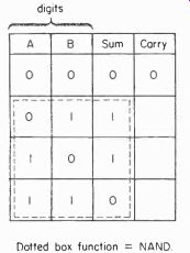
Figure 57. Binary addition truth table.
Dotted box = XOR function.
Corry is almost inverse of Sum except when A = B = 0.
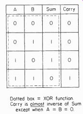
Figure 58.
A and B are 0, then the sum and carry are 0. Or to rephrase:
NOT 0 AND 0 NOT AND is NAND, so that the function of a half adder consists of XOR plus NOT plus NAND (see Figure 59). Compare with Figure 36. The drawings are slightly different, but they are logically identical.
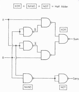
Figure 59
+++++++++++++++++++++
Circuit Forty–Eight
DIVIDE BY 4, IN QUADRATURE OUTPUTS CIRCUIT
This is an advanced application which uses a 7473 Dual Master Slave J.K. flip-flop, to generate two frequencies in quadrature, i.e. there is a 90° phase difference. The input frequency is four times the output frequencies.
This circuit together with circuit forty-nine V.C.O. forms the basis of a P.L.L. stereo decoder. The Figure 63 shows the skeleton circuit of a complete P.L.L. decoder which can be built using T.T.L. circuits. It must be emphasized that this is an advanced project requiring the use of an oscilloscope - see Figures 60,61,62 and 63.
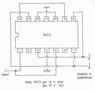
Figure 60.
4 Outputs in quadrature
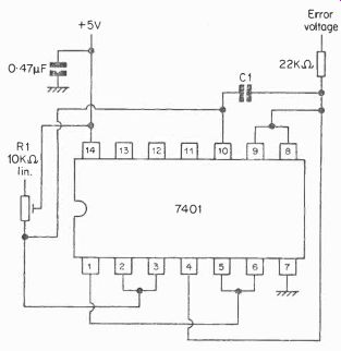
Figure 61
Most of the required circuits are featured in this guide, constructors will have to design the decoding matrix themselves.
The circuit suggested is similar to the MC1310, but anyone can build a decoder using the MC1310! The V.C.O. operates at 76 kHz.
Circuit 48 produces two 19 kHz ops, one of these is locked onto the 19 kHz pilot tone and the error voltage controls the 76 kHz V.C.O.
For those who wish to experiment further, the 74121 mono-stable can be used as a low distortion F.M. demodulator. The 74121 time period must be set to less than the time occupied by one cycle at 10.7 MHz (I.F. frequency). If the I.F. is heavily limited so that the input is a series of pulses around 10.7 MHz, level about 0.5V, to the 74121 the output will be a series of pulses of constant width where frequency corresponds to the audio frequency. If this is fed via a suitable INTEGRATING R.C. network, the output will be a precise replica of the original audio modulation.
7 = 0V
14 = +5V
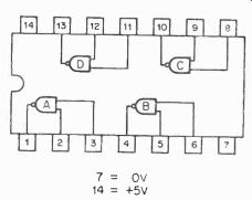
Figure 62. 7401 I.C.
+++++++++++++++++
Circuit Forty–Nine
EXPERIMENTERS V.C.O.
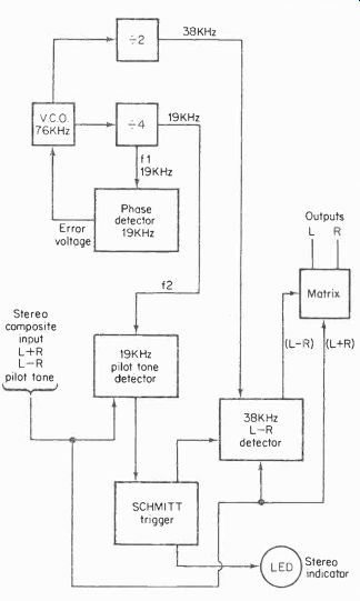
Figure 63. Experimenters T.T.L. stereo decoder.
This is an experimental V.C.O. (voltage controlled oscillator) which will work at frequencies up to several MHz by altering the value of C1. For use in a P.L.L. stereo decoder the nominal frequency is 76 kHz. Try C1 at 2200 pF to 4700 pF.
R1 is the fine frequency control. The error voltage from the phase detector is fed via the 22 k ohm resistor (see Figure 31). This is an experimental circuit and may require adjustment of circuit values in order to achieve best performance, in particular CI may vary and be outside the range indicated.
The 7401 I.C. used is a four 2 -input NAND gate I.C., which has an "open collector" output and differs from the 7400 (see Figure 62). Gates A, B and C form the V.C.O.
++++++++++++
Circuit Fifty
SHIFT REGISTER
This circuit uses a dual Flip -Flop in a shift register. Two LEDs indicate the operation of the flip-flops. Several 7476s can be cascaded to form a shift register (see Figure 64).
Note that the 7476 is a I6 -pin D.I.L. I.C.
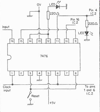
Figure 64.