The field-effect transistor (FET) is an active "voltage" device. Unlike bipolar transistors, FETs are not current amplifiers. Rather, they act much like vacuum tubes in basic operation. FETs are three-lead devices similar in appearance to bipolar transistors. The three leads are referred to as the gate, source, and drain. These three leads are somewhat analogous to the bipolar transistor's base, emitter, and collector leads, respectively. There are two general types of FETs: junction field-effect transistors (JFETs) and insulated-gate metal oxide semiconductor field-effect transistors (MOS FET or IGFET).
FETs are manufactured as either N-channel or P-channel devices. N channel FETs are used in applications requiring the drain to be positive relative to the source; the opposite is true of P-channel FETs. The schematic symbols for N-channel and P-channel JFETs and MOSFETs are shown in Fig. ---1. Note that the arrow always points toward the channel (the interconnection between the source and drain) when symbolizing N channel FETs, and away from it in P-channel symbologies.
All types of FETs have very high input impedances (1 M-ohm to over 1,000,000 M-ohm). This is the primary advantage to using FETs in the majority of applications. The complete independence of FET operation from its input current is the reason for their classification as voltage devices. Because FETs don’t need gate current to function, they don’t have an appreciable loading effect on preceding stages or transducers.
Also, because their operation does not depend on "junction recombination" of majority carriers (as do bipolar transistors), they are inherently low-noise devices.
FET Operational Principles
The basic operational principles of FETs are actually much simpler than those of bipolar transistors. FETs control current flow through a semi conductor "channel" by means of an electrostatic field.
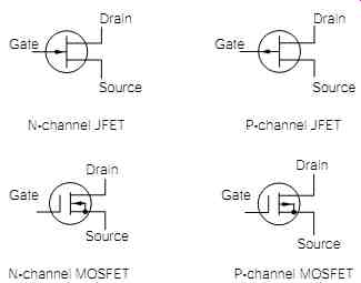
FIG. 1 JFET and MOSFET symbols.
Referring to Fig. ---2, examine the construction of a JFET. Notice that there are two junctions, with the P material connected to the gate, and the N material making up the channel. Assume that the source lead is connected to a circuit common, and a positive potential is applied to the drain lead. Current will begin to flow from source to drain with little restriction. The N-channel semiconductor material, although not a good conductor, will conduct a substantial current.
Under these conditions, if a negative voltage is applied to the gate, the PN junctions between the gate and channel material will be reverse biased (negative on the P material). The reverse-biased condition will cause a depletion region extending outward from the gate/channel junctions. As you might recall, a depletion region becomes an insulator because of the lack of majority charge carriers. As the depletion region spreads out from the gate/channel junction deeper into the channel region, it begins to restrict some of the current flow between source and drain. In effect, it reduces the conductive area of the channel, acting like a water valve closing on a stream of flowing water. This depletion region will increase outward in proportion to the increase in amplitude of the negative voltage applied to the gate.
If the negative gate voltage is increased to a high enough potential, a point will be reached when the depletion region entirely pinches off the current flow through the channel. At this point, the FET is said to be "pinched off" (this pinch-off region is analogous to cutoff in bipolar transistors), and all current flow through the channel stops. The basic principle involved is controlling the channel current with an electrostatic field. This field effect is the reason for the name field-effect transistor.
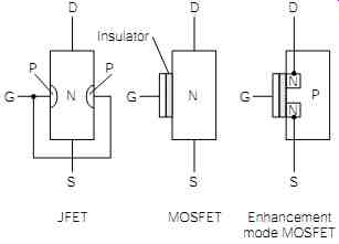
FIG. 2 FET construction. Enhancement mode MOSFET; MOSFET; JFET
Continuing to refer to Fig. ---2, notice the difference in construction between a MOSFET and JFET. Although a JFET's input impedance is very high (because of the reverse-biased gate junction), there can still be a small gate current (because of leakage current through the junction), which translates to a reduced input impedance. However, gate current through a MOSFET is totally restricted by an insulating layer between the gate and channel.
A MOSFET functions in the same basic way as a JFET. If a negative voltage is applied to the gate of an N-channel MOSFET, the negative electrostatic charge round the gate area repels the negative-charge carriers in the N-channel material, forming a resultant depletion region. As the negative gate voltage varies, the depletion region varies proportionally. The variance in this depletion region controls the current flow through the channel and, once again, current flow is controlled by an electrostatic field.
A third type of FET, called an enhancement-mode MOSFET, utilizes an electrostatic field to "create a channel," rather than deplete a channel.
Referring again to Fig. ---2, notice the construction of an enhancement mode MOSFET. The normal N channel is separated by a section of a P material block, called the substrate. N-channel enhancement-mode MOSFETs, such as the one illustrated, require a positive voltage applied to the gate. The positive potential at the gate attracts "minority" carriers out of the P-material substrate, forming a layer of "N material" around the gate area.
This has the effect of connecting the two sections of N material (attached to the source and drain) together to form a continuous channel, and thus allows current to flow. As the positive gate potential increases, the size of the channel increases proportionally, which results in a proportional increase in conductivity. Once more, current flow is controlled by an electrostatic field.
All of the operating principles discussed in this section have been applied to N-channel FETs. P-channel FET devices will operate identically; the only difference is in the reversal of voltage polarities.
FET Parameters
As discussed previously, the primary gain parameter of a standard bipolar transistor is beta. Beta defines the ratio of the current flow through the base relative to the current flow through the collector. In reference to FETs, the primary gain parameter is called transconductance (Gm).
The transconductance is a ratio defining the effect that a gate-to-source voltage (VGS) change will have on the drain current (I_D). Transconductance is typically defined in terms of micromhos (the mho is the basic unit for expressing conductance). Typical transconductance values for common FETs range from 2000 to 15,000 micromhos. The equation for calculating transconductance is:
Gm = change in drain current /ange in gate-to-source voltage
For example, assume that you were testing an unknown FET. A 1-volt change in the gate-to-source voltage caused a 10-milliamp change in the drain current. The calculation for its transconductance value would be:
Gm = 0.01 mho= 10,000 micromhos
Referring to Fig. ---3, assume that this illustration has the same transconductance value as calculated in the previous example. A 1-volt change in the gate-to-source voltage (input) will cause a 10-milliamp change in the drain current. According to Ohm's law, a 10-milliamp current change through the 1-Kohm drain resistor (RD) will cause a 10-volt change across the drain resistor (10 milliamps _ 1000 ohms _ 10 volts).
This 10-volt change will appear at the output. Therefore, because a 1-volt change at the gate resulted in a 10-volt change at the output, this circuit has a voltage gain (Ae) of 10.
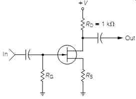
FIG. 3 JFET common-source amplifier.
In numerous ways, FET circuits can be compared with standard bipolar transistor circuits. The circuit shown in Fig. ---3 is analogous to the common-emitter configuration, and it’s appropriately called a common-source configuration. The output is inverted from the input, and it’s capable of voltage gain. If the output were taken from the source, instead of the drain, it would then be a common-drain configuration.
The output would not be inverted, and the voltage gain would be approximately 1. Of course, the common-drain FET amplifier is analogous to the common-collector amplifier in bipolar design.
FET Biasing Considerations
Referring again to Fig. ---3, note that the gate is effectively placed near the same potential as circuit common through resistor RG. With no input applied, the gate voltage (relative to circuit common) is zero.
However, this does not mean the gate-to-source voltage is zero.
Assume the source resistor (RS ) is 100 ohms, and that the drain current, which is the same as the source current, is 15 milliamps. This 15-milliamp current flow through RS would cause it to drop 1.5 volts, placing the source lead of the FET at a positive 1.5-volt potential "above circuit common." If the source is 1.5 volts more positive than the gate, it could also be said that the gate is 1.5 volts more negative than the source. (Is an 8-ounce glass, with 4 ounces of water in it, half-full or half-empty?) Therefore, the gate-to-source voltage in this case is negative 1.5 volts. This also means that the gate has a _1.5-volt negative bias. If a signal voltage is applied to the input, causing the gate to become more negative, the FET will become less conductive (more resistive), and vice versa. A JFET exhibits maximum conductivity (minimum resistance), from the source to the drain, with no bias voltage applied to the gate.
MOSFETs are biased in similar ways to JFETs, except in the case of enhancement-mode MOSFETs. As explained previously, enhancement mode MOSFETs are biased with a gate voltage of the opposite polarity to their other FET counterparts. Some enhancement-mode MOSFETs are designed to operate in either mode of operation.
In general, FETs provide a circuit designer with a higher degree of simplicity and flexibility, because of their lack of interstage loading considerations (a transistor stage with a high input impedance won’t load down the output of a previous stage). This can also result in the need for fewer stages, and less complexity in many circuit designs.
Static Electricity: An Unseen Danger
The introduction of MOS (metal oxide semiconductor) devices brought on a whole new era in the electronic world. Today, MOS technology has been incorporated into discrete and integrated components, allowing lower power consumption, improved circuit design and operation, higher component densities, and more sophisticated operation. Unfortunately, a major problem exists with all MOS devices. They are very susceptible to destruction by static electricity.
Inadvertent static electricity is usually caused by friction. Under the proper conditions, friction can force electrons to build up on nonconductive surfaces, creating a charge. When a charged substance is brought in contact with a conductive substance of lesser charge, the charged sub stance will discharge to the other conductor until the potentials are equal.
Everyone is "jolted" by static electricity from time to time. Static electrical charges can be built up on the human body by changing clothes, walking over certain types of carpeting, sliding across a car seat, or even friction from moving air. The actual potential of typical static charges is surprising.
A static charge of sufficient potential to provide a small "zap" on touching a conductive object is probably in the range of 2000 to 4000 volts! Most MOS devices can be destroyed by static discharges as low as 50 volts. The static discharge punctures the oxide insulator (which is almost indescribably thin) and forms a tiny carbon arc path through it. This renders the MOS device useless.
The point is that whenever you work with any type of MOS device, your body and tools must be free of static charges. There are many good methods available to do this. The most common is a "grounding strap," made from conductive plastic, that might be worn around the wrist or ankle and attached to a grounded object. Soldering irons should have a grounded tip, and special "antistatic" desoldering tools are available. Conductive work mats are also advisable. MOS devices must be stored in specially manufactured small parts cabinets, antistatic bags, and conductive foam.
NOTE Don’t try to make your own grounding straps out of common wire or conductive cable of any type!
This is very dangerous. It’s like working on electrical equipment while standing in water. Specially designed grounding straps, for the removal of static charges, are made from conductive plastic exhibiting very high resistance. Consequently, static charges can be drained safely, without increasing an electrocution risk in the event of an accident.
The susceptibility to static charges has led many people to believe that MOS devices are somehow "fragile." There is some evidence to support this notion; but in actuality, the problem is usually the result of an inexperienced design engineer incorporating a MOS device into an application where it doesn't belong. If properly implemented, MOS devices are as reliable as any other type of semiconductor device. However, care should be exercised in handling PC boards containing MOS devices, because some designers might extend an open, unprotected MOS device lead to an edge connector where it’s susceptible to static voltages once unplugged.
Building a High-Quality MOSFET Audio Amplifier
Many audiophiles today are adamant supporters of the virtues of MOSFETs used as output drivers in audio amplifiers. They claim that MOSFETs provide a softer, richer sound-one more reminiscent of vacuum-tube amplifiers. Although I won't get involved in that dispute, I will say that MOSFETs are more rugged than bipolar transistors and consequently provide a higher degree of reliability.
There are good economic and functional reasons to use MOSFETs as output drivers, however. At lower power levels, power MOSFETs display the same negative temperature coefficient as bipolar transistors. But at higher power levels, they begin to take on the characteristic of devices with a positive temperature coefficient. Because of this highly desirable attribute, temperature compensation circuits are not required and there is no danger of thermal runaway. Also, power MOSFETs, being voltage devices, don’t require the high current drive that must be provided for their bipolar counterparts. The result is a simpler, more temperature-stable amplifier circuit. The only disadvantage in using power MOSFETs (that I have discovered), is the lack of availability of high-power, complementary pairs.
FIG. 4 is a schematic diagram of a professional-quality 120-watt rms MOSFET audio power amplifier. If you compare this schematic with the Fig. 8-11 amplifier design, you will discover that they are very similar. Most of the same operational physics and principles apply to both designs. There are a few differences, however, which will be detailed in this section.
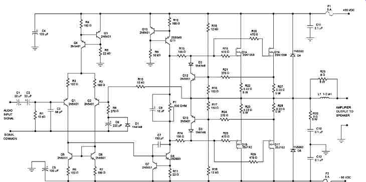
FIG. 4 Schematic diagram of a professional-quality 120-watt rms MOSFET power
amplifier .
To begin, the Fig. ---4 design incorporates four power MOSFETs in the output stage: two pairs of complementary MOSFETs that are connected in parallel with each other. This was done to increase the power output capability of the amplifier. If only about 50 or 60 watts of output power capability were desired, only a single pair of MOSFETs would have been needed. The conventional method of increasing the output power capability of any audio power amplifier, bipolar or MOSFET, is to add additional output devices in parallel.
A few of the changes incorporated into the Fig. ---4 amplifier have nothing to do with the use of MOSFET outputs-they are due to the higher rail voltages and subsequent higher output power capability. F1 and F2 have been increased to 5-amp fuses to accommodate the higher rail currents, and Q8 and Q11 have been replaced with higher dissipation transistor devices because of the higher rail voltages. Also, although not shown in the schematics, the rail decoupling capacitors (i.e., C4, C5) must have their voltage ratings increased up to at least 63 WVDC (prefer ably 100 WVDC). C10, C11, and C12 were already specified at 100 WVDC for the Fig. 8-11 project, so they are suitable for this design also. The voltage gain of this design also had to be increased in order to keep the same approximate input sensitivity. Remember, the peak-to-peak output voltage of this amplifier must be significantly greater than the Fig. 8-11 design in order to deliver about double the output power to the speaker system. Therefore, if the input signal is maintained at about 0.9 volt rms, the voltage gain must be increased. R8 was lowered to 270 ohms, which sets the gain at about 38 [(R10 _ R8) divided by R8 _ 38.03].
Now, getting into the modifications involving the incorporation of MOSFETs, note that transistor Q9 in the Fig. 8-11 diagram has been removed and replaced with a 500-ohm potentiometer (connected as a rheostat) in the Fig. ---4 diagram. Since the source-to-drain impedance values of MOSFETs increase with rising temperature, temperature compensation circuitry and dangers of thermal runaway are nonexistent.
Therefore, the V_bias temperature-tracking transistor of Fig. 8-11 (Q9) can be replaced with a simple potentiometer. Typically, P1 will be adjusted to drop about 0.8 volt to provide the small forward bias on the output devices for the minimization of crossover distortion.
Since MOSFETs are voltage devices, drawing insignificant gate currents for operational purposes, the pre-driver transistors (Q14 and Q15 in Fig. 8-11) have been removed. Unfortunately, MOSFETs do suffer the disadvantage of fairly high gate capacitance (up to about 1000 pF in many devices), which can create parasitic RF oscillations in the gate circuits (i.e., destructive high-frequency oscillations localized in the gate circuitry and not a function of the overall amplifier stability characteristics). This is especially problematic if you are using paralleled output pairs, such as in the Fig. 4 design. The cure for this idiosyncrasy is to install gate resistors, commonly called gate-stopper resistors, to provide resistive isolation from one gate to another. This is the function of resistors R19, R20, R25, and R26.
Note that C9 in Fig. 8-11 has been deleted in the Fig. ---4 design. As you may recall, C9 was implemented to improve the turn-off speed of the bipolar output transistors (eliminating the possibility of switching distortion). Unlike bipolar transistors, MOSFETs don’t have a junction capacitance mechanism that can store charge carriers and inhibit their turn-off speed. This is the reason why power MOSFETs are superior to power bipolar transistors for high-frequency applications. Therefore, C9 is not needed.
The MOSFET devices specified for the Fig. ---4 amplifier (i.e., 2SK1058/2SJ162 pairs) are a special type of MOSFETs commonly called lateral MOSFETs. These devices are specifically designed for applications in audio power amplifiers, and they will provide better performance with greater reliability than the more common HEXFET or D-MOSFET families. However, these other device types are incorporated into quite a few commercial MOSFET amplifiers because of their lower cost-lateral MOSFETs are comparatively expensive.
The performance of the Fig. ---4 audio power amplifier is quite impressive. Most of the performance specifications are virtually identical to those of the Fig. 8-11 amplifier, but the percent THD (total harmonic distortion) is a little higher, measuring out to about 0.02% at 120 watts rms. One reason for this slightly higher distortion figure is the inherent lower transconductance of MOSFETs in comparison to bipolar transistors. (Bipolar transistors can be evaluated on the basis of transconductance just like MOSFETs, but their gain factor is usually looked at from the perspective of current gain rather than transconductance.) The point is that bipolar transistors have a gain capability much higher than do MOSFETs, so their higher gain can be converted to higher levels of "linearizing" negative feedback, which results in a little better distortion performance.
I included the amplifier design of Fig. ---4 in this section primarily for discussion purposes, but it can be considered an advanced project if you want to invest the time and money into building it. However, I certainly don't recommend it for a first project. In case you believe that your construction experience and safety practices are satisfactory for such an endeavor, I have provided the following construction details.
If you design a PC board for this project, don't worry about trying to make it overly compact-the heatsinking for the MOSFETs will take up most of the enclosure space. Make sure that all of the high-current PC board tracks are extra wide. The heatsinking for the lateral MOSFETs will need to be approximately doubled over that needed for the Fig. 8-11 amplifier. (MOSFETs are a little less efficient than bipolar transistors, but they can also tolerate higher temperatures than bipolar transistors.) If you have to run fairly long connection wiring to the MOSFET leads (i.e., over _ 6 inches), it’s best to solder the gate resistors directly to the gate leads of the MOSFETs and insulate them with a small piece of heat shrink tubing. Two small heatsinks should be mounted to transistors Q8 and Q11. The remaining construction details are essentially the same as for the Fig. 8-11 amplifier design.
The raw dual-polarity power supply that you will need to power this amplifier will be quite hefty. The power transformer must be an 80-volt center-tapped model with a secondary current rating of at least 4 amps (i.e., a 320-VA transformer). I recommend a 25-amp bridge rectifier (over rated because of the high surge currents involved) and about 10,000 to 15,000 _F of filtering for each power supply rail. These capacitors will need to have a voltage rating of 75 WVDC. The AC line fuse (on the primary of the power transformer) should be a 3-amp, 250-volt slow-blow type, and don't forget to incorporate bleeder resistors.
During the initial testing of the Fig. ---4 power amplifier, or almost any power amplifier design that you want to test, the "lab quality power supply" project (the first project in this guide) can be used to detect major faults or wiring errors in the amplifier circuitry.
The power amplifier under test can be connected up to the dual polarity 38-volt outputs of the lab supply and functionally tested without a speaker load. Most modern audio power amplifier designs will function at much lower rail voltages than what they might be designed for. Obviously, under these conditions, the amplifier won’t operate at maximum performance levels, but it’s a less risky means of testing a newly constructed amplifier (or an amplifier that has just undergone major repairs). If you have made any catastrophic mistakes, the current-limited outputs of the lab supply will reduce the risk of destroying a large quantity of expensive components through collateral damage.
Circuit Potpourri
Time for more practical fun.
Sounds Like Fun
FIG. 5 is my favorite project in this guide. It can actually be "played" similar to a musical instrument to produce a variety of pleasing and unusual sounds. It’s also capable of running in "automatic mode" for unattended fascination.
The heart of this light-controlled sound generator is the basic UJT oscillator illustrated in Section 9, Fig. 9-9. Referring to this illustration, the 4.7-Kohm resistor in series with P1 is replaced with a photoresistor.
Three such oscillators are needed for the Fig. ---5 circuit. Each oscillator should have a different C1 value; the lowest C1 value chosen should be placed in oscillator 1 (to produce the highest audio frequency), the inter mediate value in oscillator 2, and the highest capacity value (producing the lowest frequency) in oscillator 3.
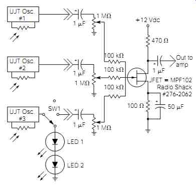
FIG. 5 Light-controlled sound generator.
The outputs of the three oscillators are capacitor-coupled to the input of a JFET audio mixer. The output of the mixer is connected to a line level input on any audio amplification system.
The P1 potentiometer in each oscillator is adjusted for a good reference frequency under ambient lighting conditions. By waving your hand over the photoresistor (causing a shadow), the frequency will decrease accordingly. With all three oscillators running, the waving of both hands over the three photoresistors can produce a wide variety of sounds. By experimenting with different P1 settings in each oscillator, the effects can be extraordinary.
Another feature, added for automatic operation, is two "high-brightness"-type LEDs on the output of oscillator 3. Referring to Fig. ---5, when SW1 is in the position to connect the oscillator 3 output to the LEDs, the LEDs will flash on and off at the oscillator's frequency. If these LEDs are placed in close proximity to the photoresistors used to control the frequency of oscillators 1 and 2, their frequency shifts will occur at the oscillator 3 frequency. In addition, even subtle changes in ambient light will cause variances. The possibilities are infinite.
Although not shown in Fig. ---5, you will need to add some series resistance between the output of oscillator 3 and the LEDs to limit the current to an appropriate level (depending on the type of LEDs used).
This circuit works very well with the 12-watt amplifier discussed in Section 8. Placed in an attractive enclosure, it’s truly an impressive project.
The JFET mixer ( Fig. ---5) is a high-quality audio frequency mixer for any audio application. If additional inputs are needed, additional 1-Mohm potentiometers and 100 Kohm-resistor combinations can be added.
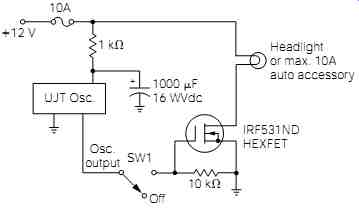
FIG. 6 Automobile headlight flasher.
Emergency Automobile Flasher
FIG. 6 illustrates how one HEXFET (a type of MOSFET) can be used to control a high-current automobile headlight for an emergency flasher.
A UJT oscillator ( Section 9, Fig. 9-9) is modified for extremely low-frequency (ELF) operation (about 1 hertz), and its output is applied to the gate of the HEXFET as a switching voltage. The 1-Kohm resistor and 1000-_F capacitor are used to decouple the oscillator from the power circuit.
Any high-current automotive accessory (up to 10 amps) can be con trolled with this circuit-even inductive loads, such as winch motors.
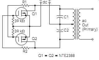
FIG. 7 Power MOSFET inverter.
Home-Made AC
The circuit illustrated in Fig. ---7 is used to convert a low-voltage DC power source (usually 12 volts from an automobile battery) to a higher voltage AC source. Circuits of this type are called inverters. The most common application for this type of circuit is the operation of line powered (120-volt AC) equipment from a car battery. There are, of course, many other applications.
For example, if you wanted to use this circuit for the previously mentioned application, the 12-volt DC source from the car battery would be applied to the DC terminals shown in Fig. ---7 (observing the correct polarity, and fuse-protecting the 12-volt line from the battery). A standard 12.6-volt ct secondary/120-volt primary power transformer is used. The VA rating of the transformer will depend on the load of the line-powered equipment intended for use with this circuit.
If the line-powered device required 120 volts AC at 1 amp ( For example), a minimum size of 120 VA is needed (I recommend using at least a 10 to 20% higher VA rating to compensate for certain losses). With the components specified, a 200-V A transformer is the largest transformer that can be used.
The combination of C1, C2, and the transformer secondary make up a resonant circuit (resonance will be discussed in a later section). Used in conjunction with the active components (Q1 and Q2), this circuit becomes a free-running oscillator, with the frequency of which is deter mined primarily by the value of C1 and C2. The transformer will operate the most efficiently at about a 60-hertz frequency, so the value of C1 and C2 should be chosen to "tune" the oscillator as closely to that frequency as possible.
Capacitors C1 and C2 should be equal in capacitance value. Start with 0.01 _F for C1 and C2, and use a resistance value of 100 K-ohms for R1 and R2. These values should bring you close to 60 hertz. If the frequency is too high, decrease the values of the capacitors slightly and vice versa for a lower-frequency condition.
============