By themselves, the audio signals produced at the microphone cannot be radiated through space as radio waves. A radio transmitter, however, is designed to amplify these audio signals and provide for them an RF carrier signal that is capable of such radiation. The audio signals are then made to vary, or modulate, this carrier in such a way that it will contain the audio intelligence. One method of doing this is for the audio signal to vary the amplitude of the RF carrier in accordance with it, and the other involves varying the frequency of the carrier. Hence, the methods are termed amplitude modulation (AM) and frequency modulation (FM) , respectively.
FREQUENCY AND PHASE MODULATION
Within the classification of FM is still another method of modulating the RF carrier known as phase modulation (PM). It is important that this method be understood in order to fully comprehend two-way radio, because it is used almost exclusively in commercial two-way radio.
The block diagram of a basic phase-modulated (PM) transmitter in Fig. 2-1 is similar to the frequency-modulated transmitter in Fig. 2-2 except for one major difference. This is the method by which the audio signal is introduced into the RF circuit. In the FM system of Fig. 2-3 the audio from the modulator is applied directly to the oscillator. This system, called "direct FM" because the oscillator is driven directly by the audio, differs from the PM system shown in Fig. 2-1. In Fig. 2-1, the audio is applied to the stage following the oscillator. This system is aptly called "indirect FM" because the oscillator output, rather than the oscillator itself, is driven by the audio.
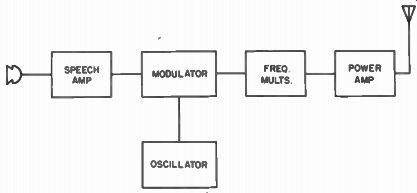
Fig. 2-1. Block diagram of a phase-modulated transmitter.

Fig. 2-2. Block diagram of a frequency-modulated transmitter.
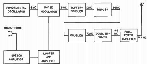
Fig. 2-3. Detailed block diagram of phase-modulated transmitter.
As stated earlier, except for the method of modulation, the two systems are identical. In both systems, the oscillator operates at much lower than the assigned channel frequency.
Therefore, a series of frequency multipliers must be used between the oscillator and power amplifier. They not only multiply the frequency, but also increase the deviation of the modulation. In addition, each multiplier stage successively increases the power of the RF signal. After the oscillator signal has been modulated and amplified, it is then applied to the power amplifier, or final, for one last tremendous boost in power. The signal is then fed into the antenna, where it is radiated into space.
BLOCK-DIAGRAM ANALYSIS
Since the phase-modulation (PM) system is used almost exclusively in commercial two-way radio, the function of each stage will be studied briefly. Later in the section a detailed study of the action of each stage will be presented. It is un necessary here to discuss "direct FM," because this system is practically nonexistent in commercial two-way radio.
The Oscillator
In analyzing the stages of the transmitter in Fig. 2-3, we will begin with the oscillator. Its primary function is to generate the fundamental RF signal necessary to drive the transmitter into production of an amplified RF signal suitable for transmission. As might be expected, since the oscillator is the source of this energy, any changes here will show up in the transmitted wave. Therefore, good frequency stability is essential in maintaining good-quality communications. If the oscillator were to drift off frequency, it might cause not only poor (or even complete loss of) communications, but interference on an adjacent channel as well. To provide this needed stability the oscillator is crystal controlled. Many manufacturers go even one step further and enclose the crystal in a heated, thermostatically controlled oven to prevent any frequency drift caused by temperature variations.
Transmitters operating at 144 to 170 mhz generally use crystals that will oscillate at 6 to 7 mhz. This signal is amplified to some degree by the oscillator tube and then coupled into the phase-modulator stage.
The Audio Amplifier
The audio signal produced by the microphone is relatively weak and must, therefore be amplified (by a conventional audio amplifier). From the speech amplifier the signal is fed into a limiter stage. The purpose of the limiter is to prevent any sharp peaks (like noise) from getting into the modulator and causing over-deviation of the RF carrier. If the signal from the speech amplifier is weak-due to an extremely weak microphone signal-the limiter will act like a conventional amplifier. However, if the signal is abnormally strong, the limiter ceases to amplify anything over a predetermined amplitude. Without the limiter, the RF carrier might be over- modulated and thus cause very poor communications. From the limiter the audio signal is again amplified in another conventional amplifier, after which it is fed into the phase modulator.
The Phase Modulator
In the phase-modulator stage the RF signal from the oscillator and the AF signal from the audio amplifier are combined.
Although the modulator here might look like a mixer or a low level modulation stage of an AM transmitter, it is actually designed to hold the amplitude modulation of the RF to the minimum. The modulator is included at this point in the transmitter to simplify the design and to reduce the audio power required to drive the modulator. Actually, the modulator can be considered a mixer of frequencies, in which two different signals are intermingled to create one composite output ready to be multiplied.
The Buffer-Doubler
The oscillator and modulator have a buffer circuit in their output to isolate them from the multipliers. Because frequency multipliers present a variable load to the preceding stage, nonlinear modulation could occur if the modulator were that preceding stage. A good buffer requires very little driving power for efficient operation. Also, the fact that its driving requirements are constant enables the modulator output to remain linear. If the modulator and oscillator worked into a changing load (like an RF amplifier or frequency multiplier) , their output requirements would likewise change and thus reflect a changing impedance into their circuits.
While the buffer input allows the modulator load to remain constant, the output circuit passes only the second-harmonic frequency of the grid signal to the next stage, thereby providing a doubling action. For example, if a 6- mhz oscillator signal were fed to the grid of the buffer-doubler, the output circuit of this stage would be designed to recognize only the second harmonic frequency of the input (6.0- mhz) signal. In this case the output would be 2 x 6.0 mhz, or 12 mhz. Furthermore, not only would the frequency be doubled, but also its deviation.
If the 6.0- mhz oscillator signal were modulated by a 1,000-cycle tone, the signal appearing at the buffer input would be 6.0 mhz plus 500 cycles, and 6.0 mhz minus 500 cycles, as shown in Fig. 2-4A. However, at the output circuit both the frequency and the deviation are doubled, as shown in Fig. 2-4B. Hence, 2 x 6 mhz equals 12 mhz, 2 x 5.9995 mhz equals 11.999 mhz, and 2 x 6.0005 mhz equals 12.001 mhz.
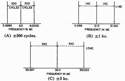
Fig. 2-4. Frequency deviation.
The Tripler
The buffer with its doubling action is only the first in a series of multiplier amplifiers. FM transmitters usually use doublers, triplers, quadruplers, or any combination of these to increase the frequency and power in steps toward the final transmitted frequency. The reason for using several stages to obtain the final frequency and power is obvious. The oscillator signal is a weak 0.2 watt or so, and there is no feasible tube that will put out a signal of 15 or 20 watts with only a 0.2 watt input. Therefore, one multiplier amplifier drives a second, the second a third, and so on. In this way the power, frequency, and deviation are gradually increased more stably and efficiently than by using only one tube (if this were possible). Following the buffer-doubler is the tripler (Fig. 2-3). Because less power output is available from any multiplier amplifier for the higher-order harmonic frequencies, low ones (usually no higher than the fourth) are utilized in multipliers.
The frequency tripler operates essentially like the preceding buffer-doubler, except that its grid and plate circuits require more input power because of the greater output power needed.
By operating the tripler (and all multipliers) in Class-C, maximum efficiency can be realized from the stage (s). Remember that the 6.0- mhz oscillator signal was multiplied to 12 mhz in the doubler. At the tripler output, the 12- mhz input signal will appear as a 36- mhz signal. This is three times the input, or six times the oscillator, signal. (The combination of the doubler times the tripler equals an increase of six.) The 36- mhz signal will now have a multiplied deviation of - ±3 khz, as shown in Fig. 2-4C. The Second Doubler As stated previously, the frequency and power in a transmitter are gradually increased in steps. Because the power is higher from one stage to the next, the design of each stage must be different. The larger the power, the higher the current carrying capabilities of the tube need be. As an example, the oscillator in most transmitters is a miniature sharp-cutoff pentode, and the second doubler is usually a miniature power pentode. Except for the increased power requirements and capabilities, the second doubler in a power-pentode arrangement operates exactly like preceding multipliers. This Class-C amplifier has its plate circuit tuned to recognize the second harmonic frequency of the grid input signal of 36 mhz -±- 3 khz. Therefore the output is 2 x 36 mhz ± 3 khz, or 72 mhz -± 6 khz.
The Double-Driver
The doubler-driver performs two important functions. First, it multiplies the signal frequency one last time before the latter is amplified by the final stage and transmitted. Secondly, the power delivered to it by the second doubler must be amplified high enough to "drive" the final RF amplifier. The twenty fourth harmonic frequency of the original oscillator signal appears in the output circuit of this stage. By multiplying the order of multipliers we see that the buffer-doubler, tripler, second doubler, and finally the doubler-driver multiply the frequency a total of 24 times (2 x 3 x 2 x 2 equals 24; and 24 x 6 mhz equals 144 mhz). Likewise, the original ± -500-cycle deviation now becomes ± -12 khz. At this time the signal is now at its final frequency, ready to be transmitted; however, the RF power is not sufficient to carry the signal very far. Different classes of power amplifiers will be encountered after the doubler-driver, depending on the type of service for which the transmitter is licensed, and also on its design.
The Final Power Amplifier
As shown in Fig. 2-3, the last stage of the transmitter is the power amplifier. Here the RF signal is boosted to the desired level for transmitting. The output power of this stage, however, is not the same in all frequency ranges, even if the same types of tubes are used. As the frequency increases, the power output capability of a tube decreases.
The efficiency of the final stage is usually 50% or better. This figure is computed by dividing the plate power consumed from the power supply (P = IE), by the measured output power in watts as read on an RF wattmeter. As an example, if a 6146 were used as a final with plate conditions of 600 VDC at 200 ma, the input power would be 600 x 0.2 equals 120 watts. At 50% efficiency, then, this stage would have an RF power output of approximately 60 watts (120 x 1 / 2 --= 60) . The output of the power amplifier is fed to the antenna, where the RF energy is radiated into space. However, the antenna and amplifiers cannot merely be connected together, because there would be a serious impedance mismatch between them. Instead, a coup ling network is needed to properly match the impedance of the RF output stage to that of the antenna system. Only then can maximum power be transferred to the antenna. (Coupling networks will be discussed in detail when the transmitter is analyzed.)
OPERATIONAL ANALYSIS
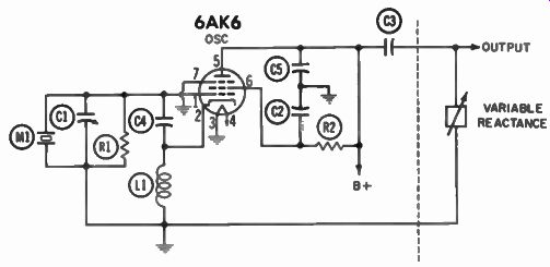
Fig. 2-5. Typical crystal-oscillator circuit.
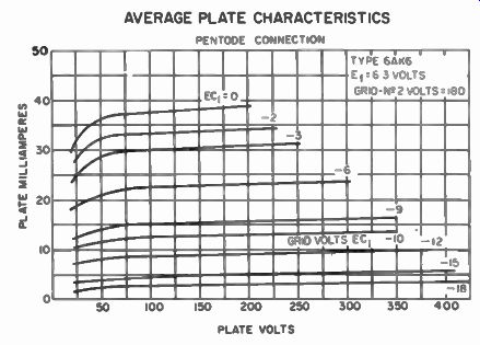
Fig. 2-6. Class-AB, operating characteristics.
Up to this point you have studied how the over-all transmitter works, what each stage does, and why. Now let's further analyze each function in order of its importance.
The Crystal Oscillator
A crystal (quartz) has the property of oscillating at many frequencies, depending on how it is cut and how it is used in an appropriate circuit. Quartz in its natural state is a relatively hard crystalline mineral. For use in radio it is first cut into thin slabs, which are then dressed down still further to a precise thickness. (The finished product is as thin as a page, of this book.) When a small voltage is placed across it, the crystal will oscillate at a definite frequency. Normally this oscillation is so weak that it must be amplified before it can be of any use.
Fig 2-5 shows a typical crystal-controlled oscillator used in two way radio transmitters. Because the crystal is merely a source of oscillations, it is not a developer of any appreciable amount of power. To subsequently amplify the signal (oscillations) , an amplifier that requires little input power must be used. This requirement can easily be met, by operating a suitable voltage amplifier in a Class-AB, mode. Class-AB, operation means the plate current of the tube flows for more than half but less than the full cycle of input-grid signal voltage. However, at no time during normal operation will the control grid be driven positive enough to draw grid current. The circuit in Fig. 2-5 is used with a 6AK6 tube in typical Class-AB, operation. Normal grid voltage is -10 volts DC, and normal cathode voltage is 0.2 volt. From Fig. 2-6 we see that with -10 volts on the grid (E4 . 1) and the plate at 200 volts, only 13 ma of plate current flows. However, when crystal M1 in Fig. 2-5 oscillates, it will drive the grid with a signal of approximately 10 volts AC peak-to-peak. Yet only about four-fifths of this 10-volt signal will cause the plate current to increase. An E,• 1 of -2 volts DC will cause approximately 34 ma of DC plate current to flow, because the 8-volt AC signal counteracted the -10 volts DC and thereby caused a net potential (during oscillation) of -2 volts to appear on the grid. This apparent -2 volts is still well below the value at which grid current will flow, so the input of the oscillator circuit takes no power from the crystal.
The actual circuit operation is as follows.
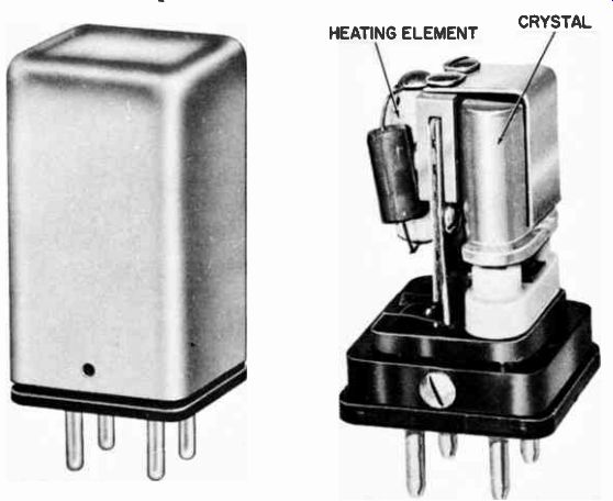
Fig. 2-7. A crystal oven. (A) External view. (B) Internal view.
In the oscillator circuit of Fig. 2-5 a resonant circuit is formed by crystal M1, C1 and R1 being in parallel with C4 and L1. Normally the potential is slightly less on the grid than on the cathode because of the IR drop across R1. However, as Ml oscillates, the IR drop will alternately be opposed and aided (according to each cycle of oscillation.) This means the tube conduction will increase when the grid signal is going positive¡ therefore, the plate current will appear as strong pulses. The frequency of these pulses appearing across C3 in Fig. 2-5 is determined by the frequency of the grid signal, which in turn is determined by the crystal oscillations.
Although the frequency of an oscillator is stabilized by using a crystal, a change in the reactance of this circuit will shift the frequency one way or the other. Notice in Fig. 2-5 that the capacitive reactance of the circuit is made variable by Cl. As C1 is adjusted from 4 to 22 mmf, the operating frequency will decrease, but will increase as C1 is adjusted from 22 to 4 mmf.
Thus the final transmitted frequency can be adjusted slightly in either direction, as required. The reactances of the circuit aren't all that will shift the frequency, though. The crystal itself (like other materials) exhibits a temperature coefficient- that is, as its temperature increases, the crystal expands, causing a corresponding change in the rate of oscillations (i.e., frequency). For this reason the crystal itself is enclosed in an oven, which maintains the crystal at a constant temperature and thereby keeps it from changing in shape. Fig. 2-7A shows a typical crystal oven. An internal view of this oven appears in Fig. 2-7B. In a circuit where good oscillator stability is important, the load presented to the oscillator must be kept constant. Like wise, the power taken from the oscillator must be constant and not too large if maximum oscillator stability is to be realized. Any amount of power taken from the oscillator reflects a low resistance into the oscillator. Therefore, the greater the power requirements, the less stable the oscillator. Most generally, the output of the transmitter is fed to the modulator and then to a buffer stage. As you know, this buffer and modulator require very little driving power, because a heavy load at the buffer input will result in nonlinear modulation. Therefore, good oscillator design is all-important if maximum efficiency is to be obtained from the unit.
The Reactance-Tube Modulator
Commercial FM two-way radio transmitters employ the reactance-tube method of modulating the oscillator frequency.
Although called FM (meaning frequency-modulated), the transmitters are actually PM or phase-modulated. However, the two are closely related because, whenever the frequency of a wave is changed, its phase (time relationship) is likewise changed and vice versa.
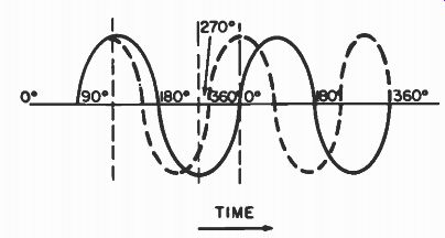
Fig. 2-8. Phase shift of a sine wave.
Notice in Fig. 2-8 that the sine wave represented by the solid line is of a certain frequency. Now if its frequency were increased by one-fourth cycle in one full cycle, you can see from the dotted line that the time displacement would be changed, and that at the end of two full cycles the new frequency would lead by almost half a cycle. It makes no difference whether the phase or frequency of the wave is changed; when one is affected the other is, too. Therefore, what is phase-modulated is really frequency-modulated; and what is frequency-modulated is actually phase-modulated. For the sake of standardization, however, the two are referred to indiscriminately as FM (frequency modulation.) Recall, in the discussion of the crystal oscillator, that any change in the reactance of the circuit parallel to the crystal will also change the frequency. This is the main principle be hind the reactance-tube method of modulation. Notice in Fig. 2-5 that there is a variable reactance across the output side of the oscillator tube. The frequency from the output side of C3 to ground will in part be determined by reactance X-as it increases the frequency decreases and vice versa.
By inserting a vacuum tube in place of variable reactance X, as shown in Fig. 2-9, and by controlling its reactance to the oscillator frequency with an audio signal applied to the control grid, the frequency across C5 can be changed. The ability of a tube to vary in reactance is due primarily to its transconductance.
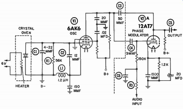
Fig. 2-9. Oscillator-modulator circuit.
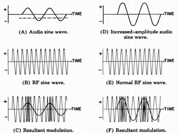
Fig. 2-10. Modulation of FM waves. (A) Audio sine wave. (B) RF sine
wave. (C) Resultant modulation. (D) Increased-amplitude audio sine wave.
(E) Normal RF sine wave. (F) Resultant modulation.
As you know from amplifier fundamentals, when an alternating signal is applied to the control grid of a tube, this signal controls the flow of electrons between the plate and cathode, and thus the transconductance. In Fig. 2-9, audio from a speech amplifier network is applied to the control grid of V2A through a 150K resistor, while RF from the oscillator is fed to the plate through C3, and to the grid through C4. This means the two RF signals will appear out of phase at the plate. A pre-distorter network (C6 and R3) is provided to shift the phase of the applied audio voltage from the speech amplifier by 90°. This is accomplished by impressing the audio through R3 and across C6. The reason for shifting the phase of the grid signal is that the frequency deviation in PM is directly proportional to the AF signal frequency; and in a phase modulator the deviation must depend only on the audio amplitude, not on its frequency.
Therefore, with this network, the audio applied to the modulator changes the response so that indirect FM (which is desired) is produced, rather than direct FM. Fig. 2-10 shows the two sine waves that are fed to the circuit of Fig. 2-9. The audio signal (A) is applied to the grid, and RF (B) is applied across the reactance tube, from plate to cathode and grid to cathode. In Fig. 2-10C the effects, in the output circuit, of the signal on the grid are shown. As the amplitude of the audio signal increases in the positive direction, the RF signal increases in frequency above its unmodulated value; and as the AF signal increases in the negative direction the RF signal decreases below the normal resting frequency.
Study the phase relationship of the RF signal in Figs. 2-10B and C. Notice in C that at the end of two AF cycles, the RF is out of phase with B. Figs. 2-10D, E, and F show the effects of a stronger AF signal on the output frequency. Fig. 2-11 shows the frequency excursion plus and minus from the carrier (resting) frequency according to the grid signal. In this manner, then, is the frequency of the transmitter modulated with the application of an audio signal to the reactance-tube modulator.
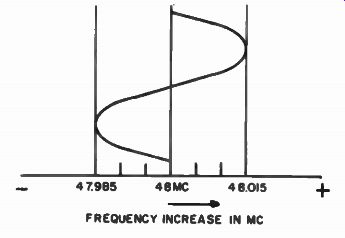
Fig. 2-11. Carrier-wave deviation.
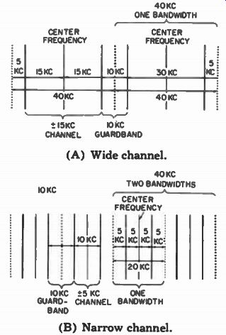
Fig. 2-12. Guard bands between channels. (A) Wide channel. (B) Narrow
channel.
The amount of deviation of the carrier frequency from its resting to its maximum plus and minus values is termed "modulation deviation"-more clearly, this is the amount of frequency change (in khz) the carrier undergoes during 100% modulation. This 100% modulation deviation is the frequency swing - ± -15 khz from the carrier in wide-band communications, and - ± -5 khz in the new narrow-channel systems. As an example, in Fig. 2-11 a center frequency of 48 mhz is modulated with a tone sufficient to produce a final deviation of ± -15 khz. With the modulator being driven into full conduction, the actual transmitter output frequency will be varied in accordance with the audio frequency. In this case, the carrier will deviate from center (48 mhz) to 47.985 mhz (-15 khz) and back to 48 mhz. Then it will go from 48 mhz to 48.015 mhz (+15 khz) With a swing of -15 and +15 khz, the transmitter is said to be 100% frequency modulated (±15 khz). In radio communications there are portions of the frequency spectrum known as "guard bands." A guard band lies between all radio channels and is 5 khz in width on either side of the - ± -15- khz carrier. This means there is a total bandwidth of 40 khz for a - ± -15- khz system. Fig. 2-12 shows the bandwidth for both the "wide" (Fig. 2-12A) and "narrow" (Fig. 2-12B) channels.
Notice that by reducing the amount of deviation in the wide channel from - -t15 to - ±5 khz in the narrow channel, twice the number of radio channels can be put on the air in the existing allotted frequency spectrum.
Frequency Multiplication
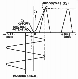
Fig. 2-13. Class-C operating characteristics.
As has been stated, the common method of multiplying a frequency is to operate a tube in Class-C condition and tune the output circuit to the desired harmonic frequency. A Class-C-operated tube is one in which the grid bias is arranged to hold the plate current well into cutoff. In this manner, it takes a strong grid signal to cause tube conduction. As you can see in Fig. 2-13, an alternating grid signal allows plate current to flow only on the positive peaks of the signal. On the negative swing of the grid, the tube is driven further into cutoff. There fore, the plate current only flows in short pulses.
A typical frequency-multiplier stage is shown in Fig. 2-14.
A series-resonant circuit (C1-L1) at the input is tuned to the frequency of the incoming signal. Another series-resonant circuit (C2-L2) is present at the output, and by selecting the proper values of inductance and capacitance in this circuit, any harmonic frequency of the input signal can be chosen. For example, a 10- mhz signal fed to the grid of a multiplier will appear as 20 mhz at the output when the latter is tuned to the second-harmonic frequency of the input signal. Frequency doublers are the most commonly used, and then triplers and quadruplers. Recall that as the order of harmonic frequencies increases, the power decreases. Therefore, usually no higher than the third or fourth harmonic frequency is utilized, be cause what is gained in frequency is lost in power. If higher frequencies are desired, additional multiplier stages are employed.
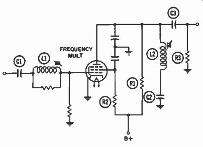
Fig. 2-14. Frequency-multiplier stage.
From the pulses of plate current in Fig. 2-13 one might believe that this is the actual signal appearing in the grid circuit of the next stage. Actually, the transferred signal must be a sine wave like that of the incoming signal in order to provide efficient Class-C operation of the next stage. As the pulses of plate current appear in the resonant plate circuit, the signal is transformed into a sine wave. Let's study this more closely to get a clearer understanding of how it is brought about.
When a pulse of plate current appears in the series-resonant circuit (L2-C2) of Fig. 2-14, C2 charges through L2. This causes a negative-going pulse to appear across C3. When the plate cuts off, the signal across C3 starts to swing positive (B+ rising). Since C2 can no longer continue to charge, it now starts to discharge through L2 and R1, causing C3 to continue in its positive direction, even though the plate is out of the circuit. The reason is that the current of C2, in discharging through L2, builds up a counter field that bucks the discharge path of C2 and thereby keeps the current flowing after plate current cutoff. Before C2 completely discharges, however, plate current again flows and thus causes the waveform across C3 to swing negative again. So you can see how the plate pulses will appear as a sine wave at the input of the succeeding stage.
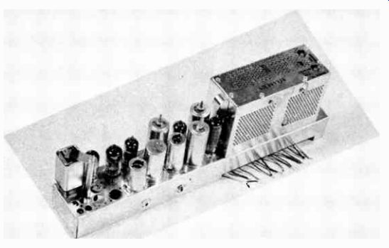
Fig. 2-15. A typical phase-modulated transmitter.
ANALYSIS OF A TYPICAL FM TRANSMITTER
The preceding sections of this section have explained the basic functions of the different parts of an FM transmitter. (Fig. 2-15 shows a typical mobile unit.) It is best to keep these fundamentals in mind when following this analysis. For the sake of clarity, the transmitter stages are presented individually.
The Speech Amplifier
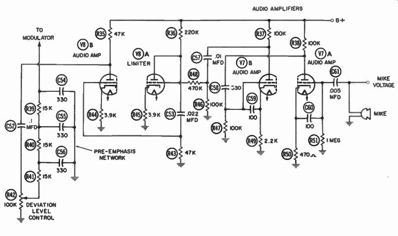
Fig. 2-16 Speech Amplifier
Fig. 2-16 shows the audio-amplifier portion of a transmitter.
With the exception of the limiting action provided by V8A and the addition of a pre-emphasis network, this speech amplifier is as simple and straightforward as any ordinary PA amplifier.
A limiter is used in transmitter audio amplifiers to prevent the carrier frequency from being over-deviated (over-modulated). The limiter amplifies and passes on to the next stage all audio signals below a preset amplitude, or strength. If loud noises picked up by the microphone were allowed to over drive the modulator, this overmodulation would distort the transmitted wave and could even cause interference on adjacent channels; so you can see the important role the limiter plays in good-quality communications.
Since the higher voice frequencies lack the intensity of the lower ones, they must be raised to the latter's level of intensity by means of a "pre-emphasis" network. When the higher frequencies are not emphasized, the audio quality will be impaired because these weak high frequencies make the greatest contribution to speech intelligibility. It is the spoken consonants rather than the vowels that are more accented, and these sounds have their energy among the higher audio frequencies.
To avoid degrading these upper frequencies, a certain amount of emphasis is placed on them in the transmitter audio circuit. To keep the recovered audio in the receiver from sounding unnatural, the reverse procedure (called "de-emphasis") is added in the receiver audio circuit. It might be thought that pre-emphasis would over-deviate the transmitter, but this is not true because the original high frequencies are merely brought up to the strength of the lower frequencies to make the audio frequencies equally strong over the entire range. The characteristics of the pre-emphasis network are shown in Fig. 2-17. Notice that the plotted curve remains relatively constant from 50 to 400 hz, and then rises abruptly to 15,000 hz.
Since this rise is specified in decibels, a change of 6 db means the signal amplitude has doubled. From this curve, then, we see that the output of the pre-emphasis network at 15 khz is almost eight times that at 1 khz.
The combination of R41-056, R40-055, and R39-054 in Fig. 2-16 is the pre-emphasis network. The audio is impressed across each capacitor in turn, through the series resistors. The output is taken off across one capacitor and applied to the next. Since the capacitive reactance falls as the frequency increases, the network output voltage rises. Actually the higher the frequency, the less reactance the circuit offers to it. Therefore, the lower and higher frequencies applied to the modulator will have approximately the same signal strength.
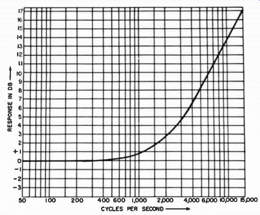
Fig. 2-17. Pre-emphasis curve.
The input from the microphone in Fig. 2-16 is developed across the 1-meg grid biasing resistor (R51) of V7A through coupling capacitor C61. This causes the grid of V7A to fluctuate at an audio rate, thus controlling the plate current. Capacitor C60 provides a certain amount of feedback from cathode to grid to stabilize the amplifier. R50 is the cathode bias for V7A, and R49 is the bias resistor for V7B. The plate load of V7A is R38, and the plate load of V7B is R37. Coupling capacitor C58 injects the amplified audio from the V7A plate into the V7B grid. C59 is the cathode-to-grid feedback stabilizing capacitor, and R47 is the grid-bias developing resistor. The output of amplifier V7B is coupled into the input of limiter V8A through C57. R46 is the limiter grid-bias resistor, and R48 keeps the grid from drawing too much current. R45 and R44 are the cathode bias resistors, and R36 and R35 the plate load resistors. The limited audio signal is coupled from amplifier V8A to V8B through C53. R43 is the grid bias resistor for V8B. From the V8B plate the signal goes through C52 into deviation level control R42, which permits periodic adjustment of the deviating audio signal to compensate for aging tubes and components. After going through the pre-emphasis network, the audio signal is then fed into the phase-modulator circuit.
The Crystal Oscillator
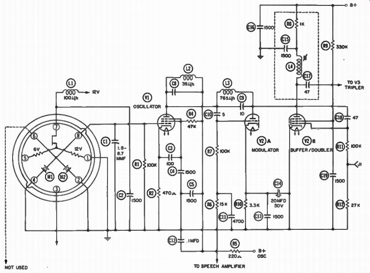
Fig 2-18. Crystal oscillator and modulator buffer-doubler.
Fig. 2-18 shows that section of the transmitter making up the oscillator modulator and buffer. The crystal oven in this oscillator has a thermostat (pin 7) in series with the 12-volt dropping heater and 12-volt filament supply. When the thermo stat contacts are closed, the heater maintains the interior of the oven at a constant temperature; no heat is developed when the contacts are open. Crystal M1 is used for oscillator V1, and M2 is in a second oscillator circuit (not shown) for use as a two-frequency transmitter. MI and frequency-adjusting capacitor C1 in parallel form the resonating oscillator circuit. RF choke L1 and capacitor C2 keep the RF (from the crystal) out of the filament circuit. Otherwise, it would cause the cathode emission to fluctuate at an RF rate and cause any number of troubles. R1 is the grid biasing resistor, and R2 is used for cathode bias. The cathode is bypassed for RF by the combination of C3 and C4 in series. C4 is the RF bypass for the screen, and C5 and C12 are the plate RF bypass capacitors. R4 is the voltage-dropping resistor in the screen-grid circuit. The combination of L2 and C8 provides enough damping action on the RF, between the screen and plate, to prevent undesired oscillations. Capacitor C10 couples the amplified oscillator signal to the phase-modulator grid, and C9 couples the same signal to the plate.
The Phase Modulator
In Fig. 2-18 the signal from the speech amplifier is fed, through pre-distorter network R6 and C11, to signal-voltage stabilizing resistor R7. At the grid of V2A, the RF from V1 and the AF from the speech amplifier are joined. The B+ for the plate comes from the oscillator circuit, and L3 blocks the modulated RF from the B+ circuit. The high cathode bias needed to operate the tube in a region of low transconductance is provided by R10. The cathode is bypassed for RF and AF by both C13 and C14.
The Frequency Multipliers
Up to this point we have dealt primarily with generating the AF and RF signals and combining them in the modulator.
From now on, however, we will be concerned with increasing the frequency, deviation, and power of the output from the modulator. The sections of the transmitter where this is done are known as the frequency multipliers.
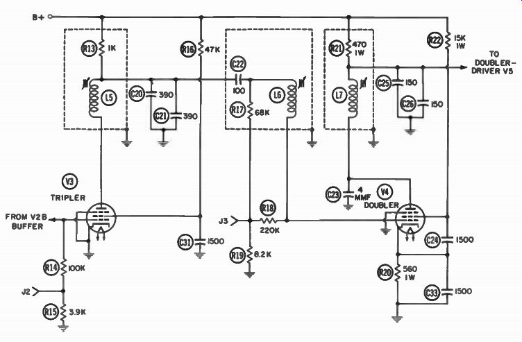
Fig. 2-19. Tripler and second doubler.
The Buffer-Doubler
From the plate of modulator V2A in Fig. 2-18, the phase modulated signal is coupled, through C18, to the grid of the buffer/doubler. This stage not only isolates the modulator from the multiplier, but is actually a multiplier itself. The signal across grid biasing resistors R11 and R12 is rectified between the cathode and grid. Since the signal swings positive enough to draw grid current, enough bias is developed across R11 and R12 to operate the tube in Class C. (J1 is a test jack for measuring the effective amount of signal present.) L4 and C15 make up the tuned plate circuit that recognizes the second-harmonic frequency of the grid signal. R8 and R9 are the plate and screen load resistors, respectively. C16 and C19, the RF bypass capacitors for the plate and screen, present a relatively low reactance to the RF and thus effectively short it to ground in these circuits. Otherwise, RF could be coupled through B+ to other circuits and thereby cause intra-stage oscillations.
The Tripler and Second Doubler
The buffer-doubler output signal, which is twice the oscillator frequency, is coupled into the tripler in Fig. 2-19. The signal is rectified across the grid and cathode via R14 and R15, and the circuit output is tuned to the third harmonic of the grid signal. Hence, the signal at the output will be six times the oscillator frequency. The LC series-resonant circuit consists of L5 and the parallel C20 and C21. The output is taken across C22, R17, and R19. To provide maximum transfer of power, the input circuit of the doubler is tunable (by L6) to the exact frequency of the incoming signal. R17 and R19 are the grid bias resistors, and R18 limits the grid current. R20 is the cathode bias resistor being bypassed for RF by C33.
R21 and R22 are the plate and screen load resistors, the series combination of C24 and C33 makes up the screen-grid RF bypass, and C23 is the plate RF bypass. The output of this doubler is tuned to twelve times the frequency of the oscillator signal. As you can see, the circuit arrangement is practically the same for all multipliers. Notice that doubler V4 handles much more plate current than V3 or V2, as seen by the use of 1-watt resistors in the cathode, screen-grid, and plate circuits.
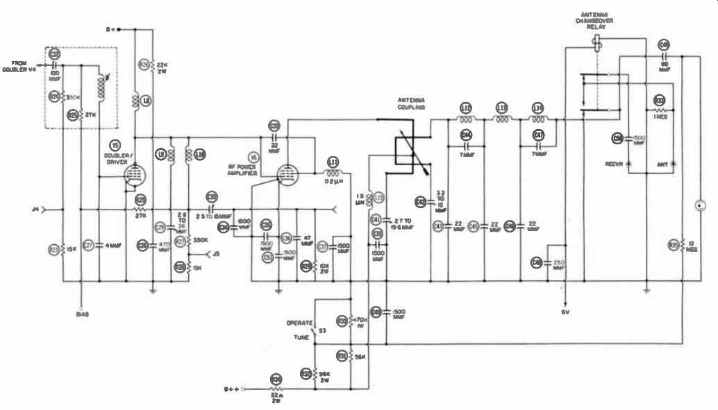
Fig. 2-20
The Doubler-Driver
Final multiplication takes place in the doubler-driver stage.
The tube used here must be capable of delivering 2 to 4 watts of RF power to the final amplifier. Unless such high-power tubes are protected by fixed grid bias from the power supply, they may be damaged should the driving signal on the grid be lost. With a loss of signal no bias would be developed, and as a result the tube would "run away" (plate current would become excessive). The circuit operation of V5 in Fig. 2-20 is the same as for the preceding stages except for the fixed bias arrangement on the grid. In addition, the output resonant circuit has a tunable capacitor instead of inductor. The reason for this is that the combination of L9 and L10 provides a fixed impedance match for the signal; hence any adjustment of these coils seriously impair the transfer of power between stages.
The RF Power Amplifier
In the RF power amplifier, the signal is boosted to the desired transmitting power. Being the last stage of amplification it is often called simply the "final." Obviously, in order to transmit as strong a signal as possible, the final not only must develop a large amount of power, but must also be capable of delivering the power efficiently to the antenna. This calls for careful circuit design and a wise choice of transmitting tubes.
The disadvantages of using ordinary triode amplifiers for finals are many: Because triodes require neutralization, additional adjustments must be incorporated which make the circuit design more critical. Moreover, since triodes have a low power sensitivity, a large amount of input power is required to produce a given output. Also, the high output capacitance of triodes reduces the tank-circuit inductance, resulting in too high a Q and thus a very narrow bandpass. At higher frequencies, tetrodes or pentodes are more useful because they provide more amplification than triodes and generally require no neutralization. With tetrode and pentode tubes, grid bias is set with reference to screen-grid, rather than plate-current, cutoff. The angle of plate current therefore depends largely on control-grid bias and screen-grid voltage. The grid voltage must never exceed the screen voltage; and during the operating cycle, the minimum plate voltages must never drop lower than the screen voltages. The presence of the screen and suppressor grids decreases the interelectrode capacitance of the tube, generally making external neutralization unnecessary. This, of course, simplifies the circuit design considerably.
The power developed in the final amplifier must be transferred to an antenna instead of another amplifier, and this antenna system has a "loading" effect on the operating Q of the plate-circuit coil. Since the antenna circuit consumes a large amount of power, the resistance presented to the output circuit of the final is extremely low; thus the Q of the coil must be low. As you can see, the Q depends on more than just the LC resonant network. For efficient operation it should be on the order of 10.
The power amplifier in Fig. 2-20 is operated as a Class-C amplifier. The input signal is taken between the grid and cathode of V6, and stable feedback is obtained from screen to control grid through C33. "Tune-operate" switch S3 is used to reduce the plate voltage (B +) to the final during alignment of the final and/or antenna circuits. The coils couple RF power from the resonant circuit to the antenna. The plate coil acts like the primary of a transformer, and the antenna is coupled in by a movable secondary which loads the antenna and thus changes the mutual inductance. You can see that a high inductance is needed here, to provide the most efficient transfer of power. For proper "loading" the antenna must be resonant at the operating frequency, and there must be a good impedance match between it and the final. If not resonant, the antenna will present a high resistance to the amplifier and thus reflect much of the output power back into the final. A bad impedance mismatch will also present a high impedance to the final. With a good antenna, adjustments C41 and C42 (along with the antenna coupling itself) will provide a high degree of power transfer.
As stated previously, a good Class-C-operated stage generates an output signal rich in harmonics. The final is a very good harmonic generator; and a suitable network suppresses these harmonics before they are radiated. The combination of C43, C44, L12, C45, L13, C46, C47, and L14 suppresses all but the operating frequency. This circuit also helps to match the output impedance of the plate circuit to the input impedance of the antenna. The antenna changeover relay permits connecting the antenna to either the transmitter or receiver. In Fig. 2-20 it is shown in the "receive" position. Notice that one of its contacts shorts the harmonic-suppressor output to ground when the transmitter (and thus the relay) is not in use. The relay is operated by depressing the push-to-talk button on the microphone. In the position shown, the antenna input to C50 and thus to the receiver is developed across 1-megohm resistor R33. When the transmitter is activated, the relay changes the antenna to the harmonic-suppressor output and opens the circuit between the suppressor and ground.
Also see: