With the background information established in the previous part, we are now ready lo tackle the final section of amplifier design, the output stage.
Although the circuitry associated with Q14 appears in the area of the driver stage on the schematic (Fig. 1 of Part 1), functionally it more properly belongs in the discussion of the output stage, which is the amplifier's workhorse. The related parameters of current, power, and heat are especially important in the output stage and there are other topics of significance as well. In this part, I will cover those important principles not already considered.
Power Rating and Amplification Class
With the power supply used, the amplifier can provide as much as 56W/channel into an 8-ohm load, so the power rating of 40W is conservative. Due to the confusion between classes of operation and the relationship between supply voltage, load current, and output power, I have included a short tutorial section on the subject.
There is a relationship between Class A operation and load impedance, reflected in the caveat that the 40W/channel Class A rating is based on an 8-ohm load.
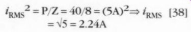
You can express power as the product of (RMS) voltage and current, or, equivalently, as the product of (RMS) current squared and load impedance. Using this latter relationship,
By definition, current flow in the output devices is never zero in Class A operation; that is, their conduction angle is 360°. The minimum current flow at a given output-power level depends on the DC bias level of the output stage.
The output stage in this amplifier is termed complementary-symmetry, which simply means that the p- and n-channel devices are complementary (equal-magnitude parameter values), and the circuit is symmetrical about the horizontal axis as drawn on the schematic. As the output is driven more positive, the upper (n-channel) transistors conduct more current, while the lower (p-channel) transistors conduct less, and vice versa as the output is driven more negative.
Load current, if positive, must be sourced from the positive power-supply rail via the n-channel MOSFETs. If negative, it must sink into the negative power supply rail through the p-channel MOS FETs. The load current at a given moment is always the arithmetic sum of the (positive) source current and the (negative) sink current. If no load current is flowing, this sum is obviously zero, meaning that the DC bias current simply flows from the positive rail first through the n- and then through the p-channel MOSFETs to the negative rail.
As load current increases from zero, the current sourced by the n-channel transistors increases above the DC bias level, while at the same time the p-channel transistors sink less current than the DC bias level. Thus, you must determine the magnitude of the peak load current and set the bias current accordingly. If RMS load current is 2.24A, then peak load current is 2.24 x V2 =3.17A.
Current Flow
Assume a bias current of 1.6A. The total current flow in the upper half of the output stage divides between the two n channel devices and increases from the bias level to 3.185A. At the same time, the total current flow in the two p-channel transistors in the lower half of the output stage decreases from the bias level of 1.6A to 0.015A. This 0.015A is sourced by the n-channel MOSFETs.
For negative peaks, the situation would reverse, with the p-channel devices sinking 3.185A from the load and 0.015A from the n-channel devices. The n-channel MOSFETs would be nearly, but not quite, in cutoff. Since there is some current in all output devices at all times, Class A operation is achieved. It follows from the power formula that lowering the load impedance increases the RMS, and, in turn, the peak load current and consequently the required Class A DC bias level.
The voltage magnitude under load ultimately determines the power rating of an amplifier, regardless of the class of operation. This is because, given the load impedance, the load current is limited by the load voltage according to i = v/Z (Ohm's law). The peak-load voltage level is a function of the supply voltage powering the output stage minus the voltage drop across the output devices and any ohmic losses due to wiring. If you could maintain the full 30V supply voltage under load without any voltage drops between the supply and the load, the amplifier could hypothetically deliver :
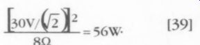
[39]
However, this hypothetical amplifier would still operate in Class A only up to the 40W level because of the DC bias current of 1.6A. Between 40 and 56W, it would operate in Class B because the output transistors would not conduct 100% of the time. An amplifier operated in Class A does not increase its power consumption when driving a load. Conservatively, you use a nominal 30V bipolar supply for the A40M output stage, but this voltage tends to drop as the power to the load increases beyond 40W and Class B operation occurs.
In Class B operation, average power delivered by the power supply does increase with increasing signal level. The magnitude of the drop is inversely related to the "stiffness" of the supply, which, in turn, is related to the power transformer, rectifiers, wiring resistance, and the filter capacitors. A sine wave with magnitude greater than the supply voltage cannot be reproduced, and the top of the sinusoidal waveform would flatten at 30V. This flattening, called "clipping," is the cause of the rapid rise in THD seen as the amplifier exceeds its rated power output.
Also note that if there were a 4 -ohm load, the output devices would still conduct 100% of the time only if the peak current were limited to less than 3.2A. This means the A40M has a Class A rating of only i2Z = (2.24)% x 4 = 20W into a 4 -ohm load, but it can deliver vy, */Z= (19)% = 90W into such a load before clipping.
Note that clipping occurs at + / - 19 __/2 =27V, because of sagging of the power supply voltage in the A40M when drawing Ipye= V90/4 = 4.7A.
What usually happens is that the output power almost, but not quite, doubles as the load impedance is halved. Increasing losses at the higher current level associated with lower load impedance is the reason that power doubling is not fully achieved. For the A40M, clipping doesn't occur until + / - 30V when driving an 8-ohm load, which well illustrates this principle. It should be clear from this discussion that the power-supply voltage and DC output-stage bias-current level were chosen to produce a 40W amplifier for 8-ohm loads that could operate in Class A up to its rated power.
Efficiency
The theoretical maximum efficiency of a Class A amplifier occurs when it is delivering its rated maximum output to a load. Efficiency is the ratio of power de livered to the load to power provided by the supply. As noted previously, the power-supply delivery is independent of the signal level when operating in Class A below the clipping level. The supply voltage is obviously constant, and the supply current simply divides between load and output devices with the sum remaining constant. Efficiency is usually expressed in percent and is denoted by 1.
For a single-ended output stage, the quiescent or DC bias current must equal the peak AC load current because a single device or a single set of paralleled devices provides all of the load current. If these devices are not to experience cut off at any time, then the (non-clipping current swing is limited to the range or I]
This quiescent' quiescent quiescent age f- is used, then-ignoring drops in the output devices-the quiescent volt py a - > 1 1 age at the output is %2Vg, , . The load voltage swing at the rated output is
+1 15 V2 2Vupplyr OF V2 p501/¥2 RMS.
The load power at rated output is thus VII supply quiescent' V2] = ) =[V I load [V supply quiescent! '"
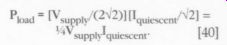
[40]
The power-supply power is V cent» and efficiency is, therefore, supply Lquies Nsingle« _- a=0 AV supply l quiescent)' )x 100 =25%.
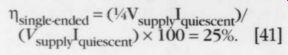
[41] V, supply h quiescent The idle-power dissipation would be more than 320W (160W/ch) if the A40M were in a single-ended design.
The situation is much better for push pull Class A output stages. Since only half the load current passes through either the upper or lower half of the output stage, idle current needs to be just 2 of the peak load current; i.e., peak current is twice the quiescent current, so RMS current is 21. cn/V2. Although you generally use a bipolar ( + / - ) power sup- ply with push-pull output stages, if Vaunply 1 defined as Vo, -V supply supply (+) - "supply (-)' then power delivered by the supply is still Von] quiescent aNd maximum power delivered to the load is P,, =
[v /(2ND)] [21 N2] = %V, supply quiescent supply quiescent' It follows that Npush- « fl i' quiescent)' supply] quiescent ) X 00" 50%.
The A40M needs to dissipate some what more than 80W/channel or 160W total in Class A operation at 40W/channel. There are 60 (230) V DC across and 1.6A DC through the output stage, a power dissipation of 96W/channel. The theoretical maximum efficiency is un achievable in practice.
Since the power delivered to a stage in Class A operation remains the same for any load power, it follows that the output MOSFETs in the A40M dissipate only approximately Y%(80 - 40) = 10W each when the amplifier is delivering its full 40W to an 8-ohm load. With no signal, the device dissipation is about 20W each.
The A40M actually runs cooler when it is blasting away to the Rolling Stones than when playing Delius or nothing at all.
This is certainly counter to the more common experience with most commercial amplifiers that operate Class B (ok, Class AB). A word to the wise (wives), then: to improve reliability of the A40M, the preamplifier volume control must be turned all the way up! You should be convinced by now of the inherent inefficiency concomitant with Class A operation. Enhancement-mode MOSFETs of the type used in the A40M can further reduce efficiency unless the driver stage is operated at a higher voltage than the output stage. Because Q15 Q18 are enhancement-mode devices, their source voltage will be lower than their gate voltage by at least the thresh old voltage. When these transistors are delivering maximum load current, the source is typically 4V below the gate, but this gate-source voltage varies from device to device and can be even higher.
The output-stage power supply is an unregulated bipolar supply of + / - 30V. Assuming a negligible drain-source voltage drop when the MOSFETs are delivering maximum load current, the source-and therefore the load-voltage can swing the full + / - 30V if and only if the gate voltage can reach +34 or + / - 35V. Even in the ideal case, the driver stage cannot produce a gate voltage on the output MOSFETs that is higher than the driver stage's own power-supply voltage.
For the A40M, the driver-stage power supply is also bipolar, but, at + / - 36V, it is higher than the output supply. The gate voltage for Q15-Q18 is consequently limited to about +35V. This is nonetheless high enough to allow the A40M output ...
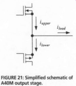
FIGURE 21: Simplified schematic of A40M output stage.
... stage to "swing the rails." Were the driver stage also operated at + / - 30V, the output could swing only + / - 25 or + / - 26V, which would result in a constant and avoidable waste of (60V -50V) x 1.6 A = 16W.
Output-Stage Distortion
If the improved efficiency is not enough reason to prefer push-pull to single ended output stages, perhaps their lower distortion is sufficient additional reason.
Because the load current is the sum of the current from the upper and lower halves of the output stage, there tends to be a partial cancellation of nonlinear distortion products to the extent that there is symmetry between those halves. For a sine input, any distortion can be expressed as a sum of all the overtones of that sine wave generated as a result of nonlinearities in the amplification chain.
In fact, this is the thrust of the Fourier series, which allows any complex repetitive waveform to be reproduced as an in finite series of harmonic components of the fundamental frequency.
If the circuit is truly symmetric, as is roughly the case with the A40M, then as drive to the n-channel MOSFETs increases to increase their drain current, drive to the p-channel MOSFETs decreases, reducing their drain current by the same amount. In this case, the total current out of the sources of n- and p-channel devices can be expressed as i_upper, and i_lower where
[43]
The terms in brackets represent the distortion, which consists of all the harmonic components of the signal that were produced as a result of nonlinearities between input and output. The presence of the term in i. merely reflects the fact that the upper and lower halves of the complementary symmetry output stage operate 180° out of phase with one another. The simplified schematic (Fig. 21) of the A40M output stage illustrates the situation.
In the absence of distortion, only the DC bias current I. cn, and the amplified version Y2Aigna1COS2E 0) of the input signal would appear in the expressions for I_upper and I... Since
I_load
upper a.lower then i quiescent +42 signal COSC2TTE ' V2{A 4c08[22nf OD] + Ay3008[3(2nf DO] +...) -
Luiescent i Y2A 00a COSC2TE t +5 V2{A 4,c08[2(2nf t + m)] + A43€08[3(2nf t+mn)]+..}=
Aggna LCOS2mf t+ 10) +
{Ag .cos[3C2nf, t+ mn) + Ayscos[5Cnf t + m)] +...) Yoad =
[44]
The trigonometric identities, cos[n(0 + pi)] = -cos if n is odd, and cos[n(6 + pi)] = cos nf if n is even, allow the cancellation of all the even harmonic terms, leaving only the fundamental, which is the desired signal, and the odd harmonic components of the distortion. The lower-order harmonic terms usually have the highest amplitudes and there fore contribute the most to the total harmonic distortion (THD). The second harmonic is canceled, and since the third harmonic probably has lower amplitude than the second, THD should be significantly reduced.
Push-Pull or Single-Ended
Advocates of single-ended Class A power amplifiers exist despite the advantages of push-pull operation shown herein. You cannot argue with subjective evaluations.
I do not consistently hear differences among well-designed amplifiers whose measured performance is in the range commonly associated with high-fidelity equipment.
In 1965, my senior engineering project was the determination of the acoustic properties of certain wall materials; I was interested in high-fidelity sound reproduction. In researching the project, I read articles in the Journal of the American Acoustical Society, as well as in several psychology journals. I recall one study in which the ability of professional musicians to distinguish between various wind instruments was impaired if they were not permitted to see the instrument (blind testing), despite the fact that the performances were live rather than recorded.
In another study, listeners were unable consistently to distinguish between live and recorded performances of small ensembles if the source of the music was not in view (again, blind testing). It seemed obvious to me at the time that knowledge of the source of a sound influences human perception of that sound.
I also know from research conducted in space flight that visual inputs to the brain very powerfully influence overall response to some non-visual stimuli. This is certainly true of the vestibular portion of the eighth cranial nerve. Although no inferences can be made, it is interesting that the other portion of the eighth nerve is the auditory portion. I suspect that the people who do hear such differences do so on the basis of such phenomena, and that I hear no differences precisely because I don't believe such differences exist.
As a physician, I have an admitted bias in favor of blind testing. I would prefer to convince myself that there is no sonic advantage to single-ended operation and to avoid the problems of in ordinate inefficiencies and measurably poorer performance. I am nonetheless glad that the controversy exists, because it is a reason to continue to explore new amplifier topologies. I might yet build a single-ended tube amplifier just for the engineering challenge such a project presents.
Cables
My opinion is that some notions prevalent in high-end circles are simply unsupportable. I offer as an example the raising of the specter of "skin-effect" in discussions about audio cables. There is a so-called "critical depth" or depth of penetration within an AC conductor at which current density will have fallen to 1/e = 0.368 of the value of the conductor's surface.
A formula for this "skin-effect" is: =
V1/(2nfop), where f is frequency in hertz,
is the conductor's DC conductivity in S/meter, and p is the permeability in H/meter. It does indicate that current density must decrease, i.e., resistivity at any depth within the conductor must increase as frequency increases. This suggests that at or above some frequency, a thin hollow tube is almost as efficacious as a solid conductor of the same diameter.
An approximate but more readily us able formula for skin effect is found in the ARRL Handbook; namely, f =124/d2, where f is now the frequency in MHz, and d is the conductor's diameter in mils (0.001"). For a 5" run of an 18 gauge conductor, resistance is about 0.032 ohm from DC up to 76kHz. It begins to rise above 76kHz, reaching 1-ohm at 100MHz. Clearly, skin effect is negligible, even at frequencies well above the audio band.
If you are nonetheless bothered by the notion of skin effect, an obvious solution is to use small-gauge cables.
Since the DC (and AC) resistance of cables increases as diameter decreases, then you will wish to parallel a number of these smaller conductors. They will need to be individually insulated so as to avoid reducing their overall surface area, and, to enhance the advantage, each of the conductors should be silver plated to increase conductivity at the critical surface region.
This is, of course, expensive, even more so because the manufacturer knows that any discerning purchaser will appreciate the difficulty of realizing truly state-of-the-art cables. You could consider some of the other claims made; cables seem to be an especially active area for imaginative marketing, usually with the assertion that phenomena that significantly apply only at RF and higher are important for audio. However, this is primarily an article about amplifier design, and I digress. Obviously, I prefer to spend my money elsewhere.
Sensitivity
You can now compute the desired sensitivity of the amplifier, i.e., the ratio of the voltage at full power output into 8-ohm2 to the 1V RMS input voltage that should produce that output power. If 1V RMS at the input is to produce 40W output into 8-ohm, then this input voltage must yield

Vimsou =VP XZ =J40x8 =17.9VRMS. [45]
This indicates that sensitivity should be 17.9V/V, that is, sensitivity devolves to the voltage gain of the amplifier. Refer ring to the discussion on feedback, closed-loop voltage gain in the A40M was determined to be approximately 1/8 =22.6. It will actually be a little less than this, but acceptable in any case.
A last point is that the number of stages in the amplifier is dictated by two necessities: first, to achieve enough open-loop voltage gain to apply effective amounts of negative feedback, and second, to attain enough transconductance gain to provide adequate current to the speakers. In short, it is difficult to convert the input voltage to several amps into the loudspeaker with less than three gain stages.
If the output-current levels were not a factor, a two- or maybe even a one-stage design, a la Nelson Pass's ZEN amplifier, would be adequate. Power MOSFETs permit the construction of a reasonable single-stage amplifier of modest power-output capability. Even so, the preamplifier or other input-signal source must have an output impedance low enough to drive the hefty gate capacitance so that slew rate doesn't suffer too much. Obviously, feedback levels are low in single-stage designs, which may also add to distortion problems.
Heatsinking
Under normal circumstances, the 96W dissipation in the output stage should be shared almost equally among the four International Rectifier (IRF) power MOS-FETs Q15-Q18. They are rated at 75W at 25°C, so 24W doesn't seem unreasonable at first glance. In fact, this is high. It is tolerable only with good heatsinking.
While it might seem complicated, evaluating thermal requirements for transistors is straightforward. Heatsink design is somewhat empirical. I learned this in designing and constructing the 100W amplifier's heatsinks in order to achieve a more aesthetically pleasing enclosure. Sawing aluminum stock with a handsaw and having a radiator repair man weld the pieces together gave mean appreciation of heatsinks. Fortunately, the availability of commercial heatsinks with well-defined characteristics simplifies the amplifier designer's task considerably.
The basic thermal equation should present little difficulty to someone with the wherewithal to build a do-it-yourself amplifier. It resembles Ohm's law and is:

Tj= Ty =(theta_jc+ theta_cs + theta_SA) P. [46]
The subscripts are: J = (transistor) junction, A = ambient (usually air), C = case, and S = (heat)sink. T designates the temperature, 6 the thermal resistance, and P the power. Temperature would play the role of voltage, thermal resistance that of resistance, and power that of current. This is intuitive.
You would suspect that temperature difference "drives" heat flow across a thermal junction, that the ease of the heat flow depends upon some property of the junction (call it thermal resistance), and that the amount of heat flow through the thermal resistance-and therefore the temperature difference- would be proportional to the power dissipated. In the case of the MOSFETs here, the power is about 25W.
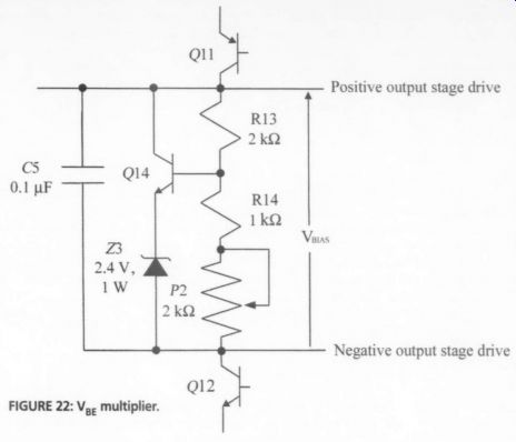
FIG. 22
According to the IRF data sheet, maximum allowed junction temperature is 150°C, but the devices must not dissipate any power at this temperature. In fact, the 75W power rating applies only for junction temperatures at or below 25°C. Above 25°C, the allowed power dissipation decreases by 0.6W/°C, which means that the highest allowed junction temperature at 25W is 25°C + (75W 25W)/(0.6W/°C) = 108°C. For long transistor life, it is advisable to keep the junction temperature well below this level.
Thermal Resistance
The overall thermal resistance is the sum of the resistances of the three thermal junctions involved. The transistor junction is thermally connected to the metal case of the transistor, creating theta_jc IRF indicates that theta_jc = 1.67°C/W. IRF also indicates that mounted to a flat, smooth, and thermally greased surface, the thermal resistance between the transistor case and that surface is just theta_cs = 0.1°C/W.
Without a heatsink, the overall thermal resistance would be that between junction and ambient air, theta_ja. For these MOSFETs, theta_ja, is a whopping 30°C/W, limiting the devices to 4W dissipation even if the ambient air temperature is held to 25°C. This certainly illustrates the requirement for a good heatsink in his application.
Companies like Wakefield and Thermalloy make heatsinks suitable for this amplifier. For example, the Wakefield 433k sink offers a thermal resistance from case to ambient of 65, = 0.37° C/W. Assuming use of this heatsink,
theta_ja = theta_jc + theta_cs +theta_sa, = 1.67 + 0.1 + 0.37 = 2.1°C/W.
In this case, the allowable transistor power dissipation would be 60W@ 25°C. At the anticipated dissipation of 25W, the junction temperature would be:
T_y=T_a +2.1°C/W x 25W =T, + 52.5°C.
If ambient is held to 25°C, then the junction temperature rises to 77.5°C.
Note that this assumes that only one transistor is mounted to each heatsink Also, the heatsink must be mounted with its fins vertical, and airflow around it must be unobstructed; else the actual junction temperature will be higher than that calculated here.
Nelson Pass likes to use the "touch" test. If the transistor case is too hot for comfort, he deems the cooling inadequate. I measured case temperatures of 80°C in normal use, and the amp does not pass the touch test. Nonetheless nearly seven years of failure-free use suggests that the design is conservative enough.
You can increase the number of devices in parallel, thereby lowering the power dissipation of each transistor, but I am not an advocate of this unless reliability is otherwise unduly compromised The reason is that each added MOSFET gate incrementally lowers the slew rate, and high-frequency distortion increases measurably.
It can be argued that paralleling more devices puts each individual device closer to the small-signal ideal of linear operation. My experience is that the high-frequency distortion increases faster due to greater capacitance than it decreases due to smaller-signal operation. Of course, if you're custom-building an amplifier, you're less likely to be intimidated by the thought of replacing a failed output transistor than if you're buying a completed amp. Commercial manufacturers must give reliability great priority.
Bias: V_BE Multiplier
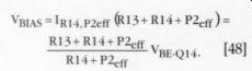
The circuit in Fig. 22 is interposed between the upper and lower halves of the driver stage. With the zener diode omit ted, it is called a Vy; multiplier and is often used in audio amplifiers in order to set the DC bias of the output stage. The operation is simple enough. Without Z3, the current through R14 and P2 would be set by the base-emitter voltage of Q14 according to:
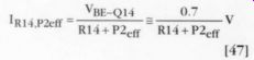
[47] I
Trimpot P2 is connected as a variable resistor, so P2_., which depends upon the position of the potentiometer wiper arm, is a resistance in the range of 0-2kQ. It is reasonable to assume that the Q14 base current is small enough that Ip 3 = Ip, 4peg It follows, then, that
[48]
The circuit multiplies the base-emitter voltage by the resistive ratio
(R13 + R14 + P2./(R14 + P2 go), hence the term Vy, multiplier.
The effect on Vy; , of the addition of zener Z3 is easily accounted for by re placing Vig 14With Ve 4+ V3 =3.7V in the equation.
As trimpot P2 is adjusted from 2k -ohm down to zero, Ip, 4preg Will increase from 1.2 to 3.7mA, causing Vg, .¢ to increase from about 6 to 11V. This Vgias range is more than adequate to set Q15-Q18 DC drain currents from almost zero to well in excess of the desired 0.8A for Class A operation.
Capacitor C5 provides a low-impedance AC path across the Vy, multiplier.
This is to help the multiplier approach the ideal DC voltage source with a voltage Vy, and zero internal (Thévenin equivalent) resistance.
Stabilizing the Bias
The zener diode can greatly improve thermal stability of Vy, ,q. In turn, this improves thermal stability of the output-stage bias current because Vy, determines the current in the power MOS-FETs Q15-Q18. Unfortunately, a Class A output stage generates a lot of heat, and thermal stability is a problem in the best of circumstances. Even the driver-stage current of up to 60mA can generate enough heat to change the bias condition on a transistor.
The V; term in the Ebers-Moll equation increases with increasing temperature. This suggests a positive tempera ture coefficient for base-emitter voltage in that Vg; must increase with increasing temperature to maintain the same magnitude of collector current. However, the reverse-saturation current I is also temperature dependent, so that Vg, actually has a negative temperature coefficient. If collector current is held constant, then Vy, changes at the rate of approximately -2.2mV/°C.
An alternative and more meaningful way of stating this from the thermal-stability standpoint is that collector current will increase with increasing tempera ture if base-emitter voltage is held constant. This fact strongly suggests that biasing a BJT by fixing Vy, will result in poor thermal stability. Looked at yet an other way, it is equivalent to an increase in BJT transconductance when tempera ture increases.
The main concern, especially in a BJT Class A output stage, is thermal runaway, in which heating due to collector current causes an increase in transconductance with still more collector current, more heating, higher transconductance, and so on. This positive thermal feed back can ultimately result in destruction of the transistor. If BJTs are paralleled, as they must be in high-power output stages, the device with the highest transconductance conducts more current initially, and the situation only gets worse as the temperature increases. This leads to "current hogging" and, again, possible destruction of the device.
Doubtful Claims
Although marketing claims give the impression that power MOSFETs have the opposite tendency-that is, that their transconductance decreases with temperature--the claims are not strictly true.
In linear applications such as this amplifier, MOSFETs also conduct more drain current as temperature increases if Vg is held constant. The channel "on" resistance does have a positive temperature coefficient that tends to provide negative thermal feedback. At very high drain currents such as those seen in switching power-supply applications, the thermal characteristics of the channel resistance dominate, and paralleled MOSFETs will share power nicely.
In linear applications, the drain currents are well below the levels seen in switching applications, so the thermal characteristics of V dominate. Similar to Vg; in BJTs, a given value of V¢ will produce higher drain currents as temperature increases. Neither Q15,Q17 nor Q16,Q18 will share power readily unless they are reasonably well-matched to one another. However, the thermally generated divergence of transconductance between these devices is so much less than that of comparable BJTs that significant current hogging is unlikely unless the devices are severely mismatched or their thermal environments are significantly different. The latter situation can occur insidiously should you incorrectly mount one of the paralleled MOSFETs on the heatsink.
All other things being equal, it is better to have all the transistors on the same heatsink. That way, any excess heat generated by one device will raise the junction temperature of its neighbors and thus improve power-sharing. I did this in my 100W monoblocks, but in the A40M prototype, I mounted each transistor on its own individual heatsink. No problem has ensued from this arrangement, but it makes reasonable matching of the output MOSFETs more important.
Zener and avalanche diode voltages are also temperature dependent, a fact you can use to good effect. For instance, the pA723 voltage regulator uses a 6.2V zener with a positive temperature coefficient of about 2mV/°C in series with a transistor base-emitter junction to create a 7V reference whose temperature coefficient is nearly zero. The purpose of Z3 in the Vg; multiplier is to reduce, but not eliminate, the overall negative thermal coefficient of V_BE-Q14 + V3.
Collector Current
The tendency of an uncompensated Vg, multiplier is to increase its collector current as its junction temperature increases. Looking at the upper driver stage, the Q11 collector current is set by Q9 and is, except for the small Early effect, independent of any circuitry attached to its collector, including the V_BE. multiplier circuitry.
The same is true in the lower driver stage consisting of Q10 and Q12. No DC current can flow into the output MOSFET gates, and, under normal conditions, no DC current will flow through the D1,Z4/D2,Z5 protection network. All DC current sourced by the upper driver circuit must flow through the V_BE multiplier circuitry and then into the lower driver.
Thus, the collector current from Q11 branches, with most of it flowing into the collector of Q14 and the remainder through R13. If I.q14 increases, Ig, 5 necessarily decreases. Reviewing the equation for Vy, , makes it clear that this will cause Vg sto fall. As it falls, the magnitude of the gate-source voltage for Q15-Q18 also falls, because V GS-Q15 =
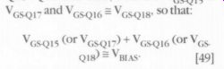
[49]
Of course, as the gate-source voltages of the output MOSFETs fall, so do their respective drain currents, along with the amplifier's Class A power rating. In this case, the temperature characteristics of Vgias actually provide (too much) thermal protection for the output devices.
This is the occasionally used thermal-protection principle, in which a diode electrically connected to the bias circuit is physically placed on an output-transistor heatsink to provide negative thermal feedback. The intention is that the presence of Z3 will provide some negative thermal feedback for output-stage protection, but not so much that the 40W Class A rating will be unachievable in a reasonably well-ventilated environment.
The drain current of the output MOS-FETs in the A40M prototype stabilizes at 0.8A if set at about 790mA at power-on.
This is an indication that the positive temperature coefficient of zener diode Z3 overcompensates the negative temperature coefficient of Q14's base-emitter voltage. You can experiment with zener diodes of different voltage if perfect or undercompensation is preferred.
Undercompensation is safer if the amplifier is to be placed in a thermally challenged location such as a confined, un ventilated area.
Overvoltage Protection
You must limit the magnitude of the gate source voltage on MOSFETs Q15-Q18 to V-GS-max <= 20V, or the device may be ruined. While 20V sounds like a very small voltage, the electric field (V/d) is enormous because of the short distance (d) between the gate and the substrate over which the voltage is dropped. The diode-zener networks consisting of D1, Z4 and D2, Z5 are designed to protect the gates of the output transistors by limiting the gate-source voltage to (less than) V_D1 + V_ZA=0.7 + 10V=10.7V.
Under normal circumstances, this voltage magnitude is limited to little more than 1/2 V_BIAS. However, the output (source) voltage can "lag" the drive voltage at the gate, a lag that can be quite significant at higher frequencies and with reactive loads attached to the output. To the extent that feedback tries to correct any errors between input and output, the potential for exceeding Vo max 18 increased. The error signal will increase driver-stage voltage to force the output to slew faster in an attempt to re duce the error.
There isn't much to limit the current if the protection network devices go into conduction, but the conduction periods should be short enough so that no dam age to the network itself occurs. The voltage limit should be high enough to preclude network activation under normal conditions of operation.
Source Degeneration--Again
Resistors R19,R20 and R23 R24 are placed in series with the sources of Q15,Q17 and Q16,Q18, respectively.
These resistors are small, just 0.1 0-ohm in value. As is clear at this point, these resistors do provide local negative feedback for the output stage and as a result help promote power sharing among the output transistors. However, since Vg for Q15-Q18 is around 4V while the DC voltage drop across any of the four resistors is just 0.8A x 0.1 ohm = 0.08V, it should be obvious that this effect is minimal.
A disadvantage is that the resistors increase the output resistance of the amplifier. This is a minor consideration, be cause they are included in the feedback loop and voltage sampling at the output reduces the intrinsic output resistance by the amount of feedback, making these already small resistors look even smaller.
Still, current flow to the load is through these resistors, and Ohm's law is unconcerned with the presence or absence of feedback. This means that the resistive voltage drop at high output can significantly reduce the load power if the resistance value is high enough. That should not be a problem here.
Why, then, even use these small source-degeneration resistors? The answer is that without them it is difficult to set output bias current or assess current sharing between the output MOSFETs. In the event of certain failures or off-nominal situations, troubleshooting is much easier if these resistors are included.
Self-Oscillation
The high input impedance and extended bandwidth of power MOSFETs make them susceptible to spontaneous oscillation when, as in the A40M, they are paralleled. The culprits are parasitic, intrinsic capacitances and inductances in the transistors. When paralleled, these parasitic elements form "tank" circuits similar to those used in RF transmitters. If you can introduce enough loss into the loop gain of such circuits, you can sup press the oscillations.
This is the purpose of gate resistors R17, R18 and R21,R22, which introduce loss, lowering the Q of the tank circuits so that no oscillation manifests. For reasons already mentioned, these resistors should be high enough, but no higher than needed to do the job. Otherwise, their presence will lower the output stage slew rate. The 220 ohm values are a good compromise.
In the 100W monoblocks, I used no base resistors in the power BJTs of the output stage. These BJTs were in CB con figuration in a kind of cascode-follower topology. Medium-power MOSFETs in ...
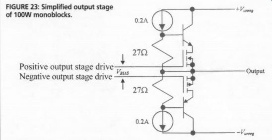
FIGURE 23: Simplified output stage of 100W monoblocks. Positive output stage drive Negative output stage drive
... pseudo-CS configuration drove the BJTs, although the amplifier output was taken from the MOSFETs' source terminals.
The arrangement, along with the cascode-bias scheme, is shown in Fig. 23 in simplified form.
Although it is driven by constant-current sources, better cascode biasing is possible by replacing the 27 ohm resistors with 5.6 or 6.2V zener diodes. When I attempted this, a high-frequency oscillation ensued. The thought might be that this was a problem associated with glob al feedback, i.e., the feedback from output to input, encompassing all amplifier stages. In this case, however, the output was operated open-loop, with feedback only from the driver stage to the input differential-amplifier stage.
How in the world can an open-loop follower stage oscillate? The answer again lies in parasitic device elements.
The 27 ohm resistors suppress the oscillation due to the loss they introduce into the BJT base circuit. The dynamic impedance of the zener diodes was too low to provide a sufficient decrease of the circuit's Q. I avoided placing resistors in series with the bases because they could drop appreciable voltage at high output levels due to the high current drive requirements of the high-power BJTs.
I have taken pride in the fact that my amplifiers have good open-loop gain and bandwidth, yet do not oscillate. This is not always the case, even with commercial amplifiers. When you see an amplifier that is physically constructed to bring the input boards so close to the output transistors that only an inch or so of wire connects them, it might be a clue that the amplifier is otherwise sensitive to self-oscillation. In this regard, the 100W monoblocks and the A40M allow considerable leeway in physical construction.
I have already discussed a possible limitation on output-voltage swing due to in sufficient driver-stage voltage swing.
There is another possibility of avoidable output-voltage-swing reduction that I should indicate.
In Fig. 23, the 0.2A constant-current sources serve a purpose in addition to supplying relatively constant cascode bias for the output stage. From that standpoint, a resistor could replace each of the constant-current sources, and the amplifier would still function reasonably well, at least until it was required to de liver an output whose voltage peaks began to approach the supply rails.
Assume that the output is near the positive rail voltage of V_unreg. This would require the collector-emitter voltage of the npn BJT at the top to be close to zero, and the BJT would be close to or in saturation. A BJT is saturated when its collector-base junction is forward-biased; in this situation, the transistor is no longer in its normal active region, its collector-emitter voltage is typically less than 1V, and it is no longer behaving as an amplifier.
A resistor replacing the upper current source would connect the npn BJT collector and base, a junction that is for ward-biased or nearly so. Thus, the resistor would have almost zero volts across it and therefore little current through it, unless its value was exceedingly low. But the resistor must have enough current to furnish base drive to the power BJT, and that base current is hefty in this situation because transistor J falls as the saturation condition is approached.
The upshot is that the BJT may not be able to bring its emitter closer than sever al volts less than VV, , and, consequently, the output voltage swing would be unnecessarily limited. If the resistor value is low enough to allow the output to approach the power rail, then the quiescent current through the resistor will be about (V -6)/R. If R were sized to deliver the same 0.2A with the output near the positive rail, it would need a value of R < 1V/0.2A = 5 ohm. At quiescence, the current through this resistor would be roughly 25V/5 -ohm = 5A and this would be a poor design, indeed.
Some amplifiers use a bootstrap capacitor at the base of the output transistors.
This capacitor stores a charge that, because the voltage across a capacitor can not change instantaneously, allows the base voltage to rise above [I as the output approaches the rail. This works, but is not very elegant. Also, a bootstrap capacitor will not work at the output of a DC amplifier such as the A40M because it will ultimately discharge, and the output voltage, if held close to the rail by a DC input, will decay.
The constant-current sources used in the 100W monoblocks were simple, power-BJT-based circuits that worked up to the point where the BJT saturated.
This gave the current source an output compliance that extended down to less than 1V and allowed the monoblocks to (almost) swing the rails.
Output Protection
Some design features from my 100W monoblocks were simply and uncritically incorporated into the A40M. Diodes D3 and D4 were included in the mono blocks to protect them from voltage reversal across the output stage. Since the power MOSFETs have intrinsic diodes, D3 and D4 can be deleted.
Stability Again
This amplifier discussion ends with the series circuit consisting of C6 and R25 that shunts the output. If you're designing an audio power amplifier, you must be sure that it will remain stable under any load conditions. In the absence of output circuitry such as that which C6 and R25 provide, some amps will exhibit high-frequency oscillations under certain load conditions. This series combination will roll off the output at high frequency, as you shall see.
Along with the output impedance of the amplifier, C6 and R25 form a net work with a zero at:
f, = 1/[2r(R25 x C6)] = 160kHz, and a pole at f = 1/{a[2n(R25 x C6)]},
where a = 1 +r /R25, ignoring z,.,. the reactive component of the amp's output impedance.
The presence of R25 and C6 thus has no significant effect on amplifier operation in the audio frequency band. In fact, because of negative feedback, r_ << 1-ohm at audio frequencies, leading to a = 1=f, = L, with apparent pole-zero cancellation. The filter does not even appear to exist as long as feedback keeps r_, small. This should out = 0 means that the amplifier output is close to the ideal voltage source, ensuring that the output-node voltage will be unaffected by any load.
At high frequencies, feedback diminishes and r_, increases concomitantly.
You can no longer ignore the pole at for since voltage division between amplifier output resistance and the R25/C6 net work occurs with consequent attenuation of the output. The zero simply means that the output load imposed by the network will never drop below the value of R25. The situation is actually more complicated than this because, as stated, the reactive component of z has been ignored.
In testing the 100W monoblocks into various loads with and without such a network, I never saw a difference in amplifier behavior. However, Nelson Pass has assured me that there is a load out there somewhere that will require the network. Also, I have yet to see an audio power amplifier that did not include come as no surprise, since r out one, so I am loath to omit it. I will welcome reader feedback about the efficacy of such networks.
Many audio power amps also include a small inductor in series with the load.
Since an inductor offers increasing op position to current flow as frequency increases, this, too, can serve to roll off output at high frequency. Such series inductors are by no means ubiquitous, and the A40M does not require one. I have seen commercial designs that exhibited ringing due to the Q of the inductor. The cure for this is to parallel the inductor with a small noninductive resistor in order to lower Q and suppress the ringing.
REFERENCES:
5. Saldahha, E. L. and Corso, John F., "Timbre cues and the Identification of Musical Instruments," Journal of the American Acoustical Society, Vol. 36, No. 11 (1964).
6. Berger, Kenneth W., "Some Factors in the Recognition of Timbre," Journal of the American Acoustical Society, Vol. 36, No. 10 (1964)
7. "The Ear as a Frequency Analyzer," Journal of the American Acoustical Society, Vol. 36, No. 9 (1964)
8. The ARRL Handbook for Radio Amateurs, The American Radio Relay League, 1997 (pp. 10, 12)
Also see: