Some of the most important functions in the signal processing chain of a
sound reproduction system are performed by the phono preamplifier.
This circuit must amplify signals from millivolt level to peak levels of two to three volts or more in order to drive a power amplifier. In addition, the circuit must equalize the signal to correct for a nonuniform frequency response which can vary by as much as 40 dB over the 20 Hz to 20,000 Hz frequency band. It must do this while introducing a minimum amount of electronic noise, and it must contend with a phono cartridge whose output impedance can vary by as much as a factor of 60 to one over the audio band.

Of particular importance are the high-frequency and transient overload characteristics of the preamplifier. Before a signal enters the preamp input, it has been processed by the RIAA recording equalizer, the constant velocity disc recording process, and the time derivative response of the magnetic playback cartridge.
The combination of these three can create input signal levels which are 100 times as great at 20,000 Hz than at 20 Hz. In addition, record ticks and pops, when processed by the time derivative response of the playback cartridge, can contain high-frequency components whose amplitudes far exceed those of normal signal levels.
Thus, the high-frequency overload characteristics of the preamplifier become very important considerations if transient IM distortion and slew-rate distortion are to be minimized.
This article describes an RIAA phono preamplifier primarily designed with these considerations in mind, and the author's unit is shown.
It uses a separate chassis for the power supply to eliminate hum induced by inductive coupling from the power transformer. At a one volt rms output level, the preamplifier's SMPTE IM distortion measures 0.004%. Its A-weighted signal-to-noise ratio is 84 dB referenced to a 10 mV input signal at 1000 Hz, which could be improved if low-noise, metal-film resistors were employed in the critical input stages.
The output circuit used to drive the power amplifier output has a 10-dB gain to insure that the power amplifier is driven to full output power. This stage has a Butterworth-aligned highpass filter characteristic which has been designed to reject subsonic and inaudible frequency components below 15 Hz, which can result from record warp, offset center holes in records, turntable rumble, and acoustic feedback. In particular, vented box loudspeaker systems using high compliance drivers are very susceptible to overdrive by subsonic signals.
The rejection of these signals can produce a marked improvement in loudspeaker performance plus a decrease in power dissipation in the power amplifier. An added advantage provided by the subsonic filter circuit is the protection of the loudspeaker and power amplifier from low-frequency transients which can occur when a tonearm is accidentally dropped on a record or when an FM tuner is rapidly tuned across the band. In both cases, low-frequency loudspeaker cone motion is reduced to a minimum to prevent possible driver suspension damage or power amplifier failure.
An optional center-channel circuit is described which can be used to drive a front center-channel amplifier and speaker system. A three-channel system has long been advocated by Paul W. Klipsch as representing the closest approach to true realization of sound reproduction. The circuit is simple and can be added to the preamplifier at any time.
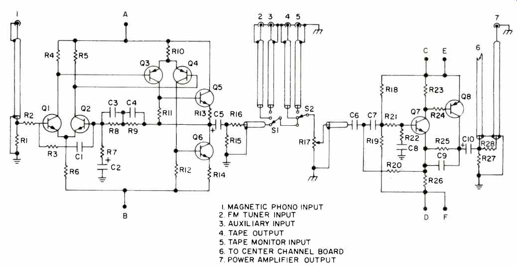
Fig. 1-Circuit diagram of the preamplifier minus power supply and center-channel
circuit.
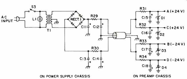
Fig. 2-Power supply circuit diagram. Note that not all components are mounted
on the power supply chassis.
Circuit Description
The circuit diagram of the preamplifier minus the power supply and optional center-channel circuit is shown in Fig. 1. It has input switching facilities for magnetic phono, FM tuner, and auxiliary inputs, and outputs for tape recorder and power amplifier. In addition, a separate tape monitor switch is provided for tape input. The volume is controlled by a potentiometer which effects only the signal level to the output stage which drives the power amplifier output jack. The circuit uses positive and negative balanced power supplies which are separately regulated by zener diodes for each stage.
The phono preamplifier circuit consists of transistors Q1 through Q6. An initial design used passive equalization between the cartridge and the input stage to equalize for the 75 microsecond pre-emphasis in the RIAA recording characteristic. This would have greatly reduced the high-frequency overload characteristics required in the phono preamplifier circuit. However, the approach was abandoned because of the uncertainty in the interaction of the output impedance of the phono cartridge and the input impedance of the circuit and because of noise considerations. Transistors Q1 and Q2 form an input differential amplifier. The differential amplifier configuration was suggested by Meyer [1] in 1972 for use as a preamplifier input stage. It has been suggested more recently by Holman [2] in a circuit similar to the one published by Meyer. Q1 and Q2 are biased by R6 at 50 microamperes each. This low bias current is necessary to provide low noise performance since the input stage determines the signal-to-noise ratio of the preamplifier. A potential problem associated with differential amplifiers is that of maintaining a balanced quiescent current in the two transistors. With the aid of a microammeter, the components in Fig. 1 have been chosen to insure that Q1 and Q2 are conducting balanced or equal quiescent currents.
This insures optimum distortion characteristics of the input stage since the predominant second-order nonlinearities in the base-to-emitter junction characteristics of Q1 and Q2 theoretically cancel when the bias currents in the two transistors are the same.
The output signal from the input differential amplifier is applied to a second differential amplifier which consists of transistors Q3 and Q4. In addition to supplying a second stage of voltage gain, the differential connection of Q3 and Q4 provides the very important cancellation of any common-mode noise from the input stage due to thermal noise generated by the emitter bias resistor R6. Without this feature, the signal-to-noise ratio that is established by the input stage would be inferior to that which could be achieved by employing a single-ended input stage rather that the differential configuration [3]. The signals from Q3 and Q4 drive the class-A, push-pull output stage consisting of transistors Q5 and Q6. These transistors provide the current gain necessary to drive the feedback network and the following stages of the preamplifier. Since Q5 and Q6 operate in a true class-A mode, there is nothing to be gained from the added complexity necessary to drive a complementary output stage.
The feedback network consists of resistors R7 through R9 and capacitors C2 through C4. The resistors in this network have been chosen so that the closed-loop gain at 20 Hz is 60 dB, more than 20 dB lower than the open loop gain of the preamplifier. Thus, a low-frequency feedback ratio of greater than 20 dB insures an extended low-frequency response with low distortion characteristics. C2 has been chosen so that the lower minus 3-dB frequency of the phono preamplifier circuit is less than 1 Hz. If the circuit is used to drive a power amplifier without the 10-dB gain output circuit, it is recommended that C2 be changed from 100 microfarads to 5 microfarads in order to provide some rejection of unwanted subsonic signals. With this change, the minus 3-dB lower frequency of the phono preamplifier will be moved up to 8 Hz.
The time constants for the RIAA equalization are set by R8, R9, C3, and C4. Since the open-loop gain and bandwidth of the phono preamplifier will also effect the RIAA equalization, these elements cannot be calculated precisely, rather they must be determined experimentally for optimum equalization. The approach taken in the present case was to first calculate these components from network theory under the assumptions of an infinite open-loop gain and bandwidth and zero output impedance. The elements were then tuned experimentally to optimize the equalization. This was done with the aid of the passive inverse-RIAA equalization circuit recommended by Audio Research for the testing of preamplifiers. The experimental tuning procedure was performed by exciting the preamplifier from a General Radio pink noise source through the inverse-RIAA equalizer. The output of the preamplifier was then monitored on a Hewlett-Packard real-time spectrum analyzer, and the feedback network elements were tuned for the flattest overall equalization. The transient response of the preamplifier was also monitored during this process with a square wave input signal through the inverse-RIAA equalizer to insure that the square wave response was also being optimized.
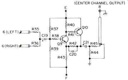
Fig. 3--Center-channel circuit diagram.
===============
PARTS LIST
Parts List for one channel. All resistors are 1/4 watt, 5% unless otherwise specified. Resistors should be carbon film rather than carbon composition unless otherwise specified.
- R1 47 kilohm, metal film
- R2 1 kilohm, metal film
- R3 390 ohm
- R4, R5 36 kilohm, metal film
- R6 220 kilohm, metal film
- R7 3.9 kilohm, metal film
- R8 330 kilohm, metal film
- R9 4.3 megohm, metal film
- R10 2.2 kilohm
- R11 5.6 kilohm
- R12 6.2 kilohm
- R13, R14 220 ohm
- R15 100 kilohm
- R16 560 ohm
- R17 20 kilohm, dual potentiometer
- R18 470 kilohm
- R19 100 kilohm
- R20 33 kilohm
- R21 4.3 kilohm
- R22 390 ohm
- R23 3.3 kilohm
- R24 100 ohm
- R25 2.2 kilohm
- R26 1 kilohm
- R27 100 kilohm
- R28 560 ohm
- R29, R30 270 ohm, 1 watt
- R31, R33 390 ohm, 1/2 watt
- R32, R34 270 ohm, 1/2 watt (200 ohm, 1/2 watt with center-channel circuit)
- R35, R36 91 kilohm
- R37 68 kilohm
- R38 3.3 kilohm
- R39 5.6 kilohm
- R40 3.3 kilohm
- R41 100 ohm
- R42 3.6 kilohm
- R43 430 ohm
- R44 100 kilohm
- R45 560 ohm
- C1 0.001 µF, 100 volt, ceramic capacitor
- C2 100µF, 10 volt, electrolytic capacitor
- C3 220 pF, 100 volt, 5% silver mica capacitor
- C4 820 pF, 100 volt, 5% silver mica capacitor
- C5 25 µF, 25 volt, electrolytic capacitor
- C6, C7 0.22µF, 25 volt, 5% ceramic capacitor
- C8 390 pF, 100 volt, ceramic capacitor
- C9 10 pF, 100 volt, ceramic capacitor
- C10 25 µF, 25 volt, electrolytic capacitor
- C11, C12, C13, C14 2000 µF, 50 volt, electrolytic capacitor
- C15, C16, C17, C18 100 µF, 25 volt, electrolytic capacitor
- C19 25 µF, 25 volt, electrolytic capacitor
- C20 10 pF, 100 volt, ceramic capacitor
- C21 25 pF, 25 volt, electrolytic capacitor
- Q1, Q2, Q5, Q6, Q7, Q9 2N5210 transistor
- Q3, Q4, Q8, Q10 2N5087 transistor
- S1 3-position, rotary selector switch (stereo)
- S2 double-pole, single-throw toggle switch
- S3 single-pole, single-throw toggle or pushbutton switch
- L1 120 volt a.c. neon pilot lamp with dropping resistor
- T1 Stancor P8605 transformer (Use Output Taps 2 and 3)
- Rect. 1 bridge rectifier, 1 amp, 100 volt
- PIV D1, D2, D3, D4 24 volt, 1 watt Zener diode
Miscellaneous
Two chassis and covers, phono jacks, power cord, phone jacks and plugs, shielded cable, knobs, screws, nuts, lockwashers, circuit board standoffs (conducting), heat sinks for Q8 and Q10, terminal strips, etc.
Printed circuit boards and matched transistors for the preamplifier are available for a limited time. Prices are $10 for a set of stereo boards for the RIAA circuits and output circuits, $5 for the center-channel board, and $1.50 for a matched pair of 2N5210 or 2N5087 transistors, plus $1 shipping and handling.
Address orders to Components, P.O. Box 33193, Decatur, Ga. 30033.
===============
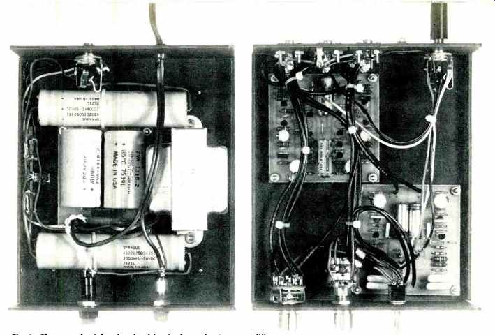
Fig. 6--Photograph of the chassis wiring in the author's preamplifier.
The overload characteristics of the magnetic phono input circuit are adequate to insure that it will not be driven into clipping or slewing during normal use. This circuit will put out a 40-volt peak-to-peak sine wave signal up to a frequency of 120 kHz, and its clipping characteristics are symmetrical under these conditions. The overload margin of a preamplifier is an important consideration, especially at high frequencies. Although limitations in disc recording make it impossible to cut large amplitude high frequency signals on records, the output of a magnetic cartridge increases with frequency at 6 dB per octave because of its time derivative response.

Normal frequency response plots for cartridges do not show this since the plots are corrected for it. However, phono preamplifiers must handle the boosted high frequencies without overload or slewing. Record ticks and pops are impulsive in nature, and thus they contain very broadband frequency spectra. In combination with the rising frequency response characteristics of the cartridge, they can easily cause high-frequency overload, transient IM distortion, and slew-rate distortion if the high-frequency overload characteristics of the phono preamplifier are not adequate. In addition, four-channel discs recorded with the CD-4 process can cause surprisingly large high-frequency sub carrier signals at the cartridge output, even if it is not designed for CD-4 use.
Although preamplifiers are not designed to put out appreciable signals at these frequencies, the high-frequency overload margin in any circuit which uses negative feedback for equalization can be seriously degraded. Thus, it is the author's opinion that CD-4 discs are best used with only CD-4 equipment.
The output of the phono preamplifier is fed through the input switching facilities in Fig. 1 to a 20-kilohm volume control. When the tape monitor switch is in the normal mode, the input impedance to any tape deck connected to the tape output jack appears in parallel with the volume control. It is recommended that only a high impedance tape deck be used with the tape output, otherwise, the total load impedance on the preamplifier circuit may drop too low.
The volume control drives the output stage which consists of transistors Q7 and Q8. The gain of this circuit is set at 10 dB by resistors R25 and R26.
The circuit is designed to have an active-filter, Butterworth high-pass alignment which is flat above 20 Hz. It exhibits a 12-dB-per-octave rolloff below its 3-dB cutoff frequency of 14 Hz.
The alignment of this filter is set by C6, C7, R18, R19, and R20. Substitute
The component layouts for the three circuit boards are given in Fig. 5.
The view in these figures is from the component side of the boards, i.e. the side opposite from the foil circuit.
There are no special instructions for mounting the components on the circuit boards. It is recommended that the transistor leads be inserted no more than 1/4 inch through the boards before soldering. This will prevent any heat damage from the soldering iron due to excessive heat conduction through transistor leads which are too short. Normal precautions should be taken to insure that all transistors, electrolytic capacitors, and diodes are inserted correctly. Otherwise, failure could result at turn on.
After all components are mounted and soldered to the boards, the next step is to solder all input and output cables and all power supply leads to each board. It is recommended that only shielded cable be used for signal input and output leads. No. 22 stranded wire should be used for the power supply leads. The connection of cable grounds illustrated in Figs. 1 and 3 should be adhered to if ground loops are to be avoided. The figures show that the shielded cable grounds are not connected at the signal inputs of either the output circuit board or the center channel board or at the tape output or power amplifier output jacks.
The main chassis should be drilled for the input selector switch, volume control, tape monitor switch, power input jack, signal input and output jacks, the circuit board mounting holes, and the external ground lug connection. The latter can be a 6-32 by 1/2 inch screw attached to the chassis with a No. 6 nut and an inside star lockwasher. The screw should be installed near the phono input jacks with its head inside the chassis and with a second nut loosely screwed down over the first nut outside the chassis. The jacks for the magnetic phono inputs should have floating ground terminals, i.e. they are not grounded to the chassis. All other signal input and output jacks should be grounded to the chassis. If these jacks have floating grounds, they should be connected to ground through a common ground bus which connects to chassis ground through a securely tightened lockwasher grounding lug.
One end lug on the volume control for each channel is grounded to chassis through a lockwasher grounding lug mounted concentric with the volume control shaft. The end lug to be grounded is that one which measures zero resistance to the center lug when the volume control is set fully counter-clockwise.
After the chassis hardware is mounted, the shielded cables from all input and output jacks which connect to the selector switch and tape monitor switch should be installed and soldered. Care should be taken when soldering the shielded cable grounds, for the heat can melt the inner cable insulation and cause the center conductor to short to ground. To minimize this possibility, the cable grounds should be soldered before the center conductors. In this way, the center conductors will not be flexed when the grounds are soldered.
The circuit boards can now be installed in the chassis as shown in Fig. 6.
These should be mounted with a 3/8 inch No. 4 metal standoff under each corner with 4-40 by '/4 inch screws and No. 4 nuts. A No. 4 inside star lock washer should be used on each end of each standoff to insure good connection of the circuit board grounds to chassis ground through each standoff. The mounting screws should be securely tightened so that the lock washers will be firmly engaged. Once the circuit boards are mounted, the remainder of the chassis wiring can be connected. Once this is done, the cables should be neatly tied so that they do not run near the circuit boards. It is preferable to route the cables down along the chassis. However, if there is insufficient room, they can be routed over the circuit boards, as has been done in Fig. 6. The final step is to attach a '/ inch by '/2 inch heat sink made from 1/16 inch sheet aluminum to transistors Q8 and Q10. The heat sinks can be glued to the flat sides of the transistors with a small dab of contact cement. None of these transistors dissipate over 180 mW quiescently, while they are rated at 310 m W. However, the heat sinks are a worthwhile and effective protection measure which will improve the reliability of the preamplifier, especially if it is operated near heat producing equipment.
The power supply is wired as shown in Fig. 2. It should be noted that not all the components in this figure are mounted on the power supply chassis.
The output power leads from the power supply chassis and the input power leads to the preamplifier chassis should be wired to a three conductor phone jack, one conductor of which is grounded to its respective chassis. A six-foot length of three conductor power cable with phone plugs attached to each end can then be used to connect the power supply to the preamplifier. The a.c. power cord to the power supply should be insulated from the chassis feed through hole with a proper size strain relief or grommet. In the latter case, an insulated cable clamp should be used to secure the power cord inside the chassis to prevent its being pulled loose.
Check Out and Turn On Procedures
Before any power is applied to the preamplifier, the entire circuit should be carefully checked. Trouble points include diodes and electrolytic capacitors installed with the incorrect polarity, transistor leads reversed, poor ground connections to chassis (especially if the chassis is painted), cold solder joints, shorted cables, etc.
After all wiring has been checked, the power supply can be checked out.
With the preamplifier power cable disconnected, apply a.c. power to the power supply and measure the d.c. voltages on C11 through C14. These capacitors should have approximately 42 volts across them with no load. At this point, the polarity of the voltage across these capacitors should be checked to verify that none is installed backward. After the power supply unit is checked out, remove the a.c. power and connect the power cable between the power supply and the preamplifier chassis. If phone jacks and plugs are used for these connections, a slight spark may be noticed when the plugs are inserted if there is a charge stored on C12 and C14. Care should be taken to insert the phone plugs fully into the jacks.
Otherwise, a short circuit to ground will occur and R29 and R30 will smoke when the a.c. power is turned on.
Before connecting any equipment to the preamplifier, power should be applied and the circuits should be checked out with a d.c. voltmeter.
First, measure the voltages across C15 through C18. These should be exactly 24 volts. Next measure the voltages across C12 and C14. These should be 31.5 volts plus or minus 0.5 volts. If these voltages are not in this range, R29 and R30 should be changed to the next higher or lower value to respectively decrease or increase the voltage across C12 and C14. Next measure the voltages from ground to the junctions of C5 and R13, C10 and R25, and C21 and R42. These should be less than one volt. If not, a wiring error has been made or there is a defective component in the circuit.
Before connecting any equipment to the preamplifier, all a.c. power to the complete system should be turned off. Connect all inputs and outputs including the turntable ground wire which attaches to the No. 6 external grounding screw on the rear of the preamplifier chassis. Since there is a slight turn-on thump caused by the charging of capacitors in the circuit, the preamplifier should be turned on before the power amplifier.
It can be left on if desired with no harm to the circuits. Normal precautions should be observed when using the preamplifier. These include never connecting or disconnecting an input or output cable with the power amplifiers turned on. Otherwise, an open ground connection can cause a large 60-Hz signal to be fed to the power amplifier when the phono jack is removed or inserted. Happy listening! References
1. D. Meyer, "A Super Op-Amp Pre amp," The Audio Amateur, Vol. III, No. 1, Oct., 1972, pp. 16-21.
2. T. Holman, "New Factors in Phonograph Preamplifier Design," Journal of the Audio Engineering Society, Vol. 24, No. 4, May, 1976, pp. 263-270.
3. C. D. Motchenbacher and F. C. Fitchen, Low Noise Electronic Design, John Wiley and Sons, N. Y., 1973.
4. W. M. Leach, "Suppression of Slew-Rate and Transient IM Distortions in Audio Power Amplifiers," presented at the 55th Convention of the Audio Engineering Society in New York, October, 1976.
Low TIM Amplifier PART II
The low transient IMD (or TIM) amplifier which has been described [1] did not contain a protection circuit in order to minimize the complexity as a construction article. A voltage-current sensing (or VI) limiter has been developed for the protection of the output stage of this amplifier from overload conditions for load impedances less than 4 ohms. In addition, a second protection circuit has been developed which protects the voltage gain stages of the amplifier in the event of a failure in the output stages.
The printed circuit foil patterns for this protection circuit were included on the circuit board layouts given [1]. The two-stage protection circuit will be described in this second part article on the amplifier. In addition, several minor modifications to the circuit will be described which improve its TIM rejection characteristics and which correct some minor errors which appeared in the first article.
Corrections to The Published Circuit
The complete circuit diagram of the amplifier with all corrections and the addition of the VI limiter is shown in Fig. 1. All changes in component values are indicated by an asterisk in the supplemental parts list. The NPN driver transistor is properly labeled Q10 rather than Q11 as was originally published. A change which should answer some questions which have arisen is shown in the bias circuit. The positions of R24, D3, D4, and D5 in Fig. 1 now correspond to those on the circuit board layout. This change has required a modification in the figure for the diode bias mounting diagram.
This is given in Fig. 2.
It has been previously published in a Letter to the Editor that use of the specified anodized heat sinks could result in an ungrounded circuit board.
To prevent this, the anodization should be thoroughly scraped or filed away beneath all lockwashers and nuts used both to attach the circuit boards to the heat sinks and those used to attach the mounting L-brackets to the heat sinks. For proper hum elimination, it is necessary to ground the circuit boards to the heat sinks through each of the four mounting screws and to ground the heat sinks through both mounting L-brackets.
The use of non-anodized heat sinks will eliminate this problem.
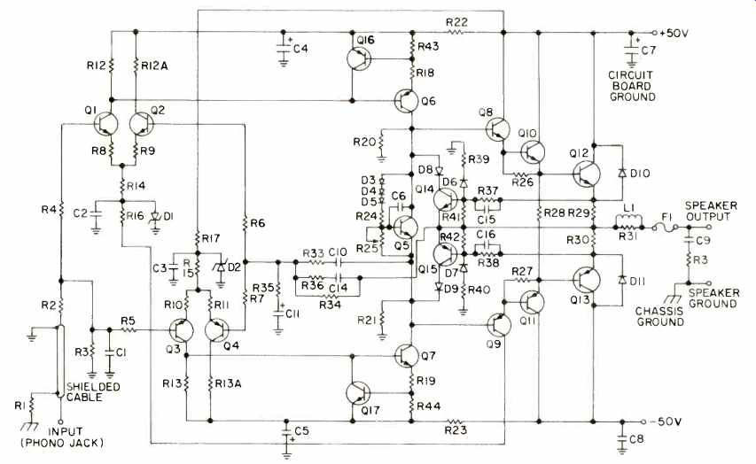
Fig. 1-Complete circuit diagram of one channel showing the modifications
to the feedback network and the voltage-current sensing protection circuit.
Modifications to The Published Circuit
The modifications to the circuit involve the time constants used in the input low-pass filter and in the TIM suppressing alternate feedback network. R2 should be changed from a 2.7 kilohm resistor to a 4.7 kilohm resistor. This change moves the 3-dB cutoff frequency of the input low-pass filter to 100 kHz from 150 kHz. This helps prevent the application of inaudible, high-frequency overload signals which could aggravate charge storage effects in the output stages.
The most important modifications which have been made involve the TIM suppressing feedback network.
As shown in Fig. 2, the 10 pF lead compensation capacitor C10 now connects to the emitter of Q5 rather than to R34. This change was necessitated when an amplifier was encountered which exhibited a marginal stability problem due to mutual coupling effects and mutual inductance in the leads which attach the output transistors to the circuit board. By connecting C10 to the emitter of Q5, the lead compensation is taken from output of the second voltage gain stage, thus bypassing any phase shifts which are encountered by the signal in traversing through the driver and output transistors and their connecting leads. The second change in the feedback network is in the value of R-36. This has been changed from 10 kilohm to 33 kilohm.
The purpose of C14 and R36 is to extend the loop bandwidth of the amplifier from approximately 38 kHz to approximately 100 kHz. This frequency coincides with the 100 kHz cutoff frequency of the input low-pass filter.
The loop bandwidth of an amplifier is that bandwidth experienced by a signal when it propagates from input to output and then back through the feedback network. Without C14 and R36, this would be equal to the open loop bandwidth which is approximately 38 kHz. In addition to the improvement in the loop bandwidth, C14 and R36 serve the function of causing the amplifier to reject inaudible high-frequency input signals which lie above 50 kHz. It is important to note that the high-frequency overload rejection is not accomplished by slowing down the amplifier loop response, but by speeding it up. It can be shown by feedback control theory that this is an elegant solution to the transient overload problem in the input stages, for it uses the feedback signal itself to cancel out ultrasonic overload signals which lie outside the open-loop bandwidth of the amplifier.
One question which has not been addressed is the effect of the TIM suppressing feedback network on the phase response of the amplifier. The phase shift is approximately 30° at 20,000 Hz. However, below 20,000 Hz, the phase decreases linearly with frequency. This means that the amplifier exhibits no group delay distortion, for its phase response corresponds to a constant time delay of about 4 microseconds. That is, all audible frequencies propagate through the amplifier with the same time delay, adding in their proper phase relationships at the output.
It can be shown that the output impedance of any negative feedback amplifier is inductive above its loop bandwidth. This has caused oscillation problems in many amplifiers with capacitive loads, for the inductive output impedance tunes with the capacitive load to form a resonant circuit. At best, an amplifier with insufficient loop bandwidth will exhibit severe ringing when driven by a square wave into a capacitive load. This problem is eliminated in the circuit of Fig. 1 by the combination of an open-loop bandwidth of approximately twice that of the audible spectrum, the input low-pass filter, and the TIM-suppressing feedback network. The amplifier will drive a 2 microfarad capacitor for a load with essentially no ringing with square-wave signals. This makes L1 and R31 unnecessary in their usual function of preventing oscillations into capacitive loads. However, their removal is not recommended since they provide some degree of r.f. protection from r.f. signals which may be picked up on the speaker lines. Capacitive load testing of amplifiers is not a recommended procedure for the inexperienced.
Next to a short circuit, the capacitor is probably one of the most demanding load tests on an amplifier. Nevertheless, the square-wave performance of an amplifier into a capacitive load is a good indicator of how well it is capable of driving dynamic speakers in the frequency range directly above their resonant frequency, electrostatic speakers, and piezoelectric speakers.
--------
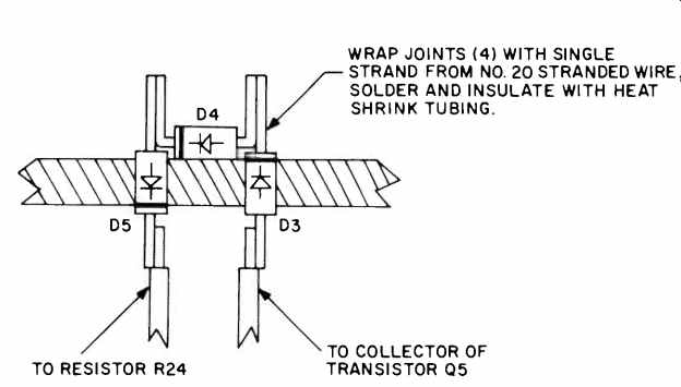
Fig. 2--Diagram showing mounting of the temperature compensating bias diodes
on the main heat sinks. The banded end of each diode is the cathode.
-----------
Protection Circuit
In Fig. 1, transistors Q14 through Q17 and their associated components form the protection circuit. Protection of the output stages is provided by Q14 and Q15. These two transistors are connected so that they sense both the current supplied by the output transistors, i.e. the voltage across R29 and R30, and the voltage on the speaker line. Speaker load impedances above 4 ohms will not cause activation of Q14 or Q15. However, for load impedances below 4 ohms, these two transistors act as current limiters to prevent excessive power dissipation and possible failure in the output transistors.
To understand the operation of Q14 and Q15, it is convenient to consider two speaker load conditions, a short circuit and an open circuit. First, for a short circuit, the current through R29 and R30 will be very large, even for small input signals. This current is sufficient to cause a voltage drop across R29 and R30 which will cause Q14 and Q15 to conduct. Their conduction reduces the drive voltage to the driver stages which in turn reduces the current supplied by the output transistors. In contrast, an open circuit on the speaker line will cause very little current to be supplied through R29 and R30, a current which is insufficient to activate Q14 and Q15. In addition, the voltage on the speaker line (which is absent when the output is short circuited) provides a reverse bias voltage at the emitters of Q14 and Q15 which helps prevent their conduction. The combination of the voltage across R29 and R30 and the reverse bias voltage at the emitters of Q14 and Q15 cause the limiter not to be activated for load impedances above 4 ohms.
The reverse emitter bias voltage for Q14 and Q15 is determined by resistors R39 and R40. These have been chosen to limit the peak current into a 2-ohm load to about 4 amperes. Into a short circuit, the peak current is limited to about 2 amperes. Thus, the peak current is a function of load impedance-the smaller the load impedance, the lower the threshold of the current limiter. The approximate relation between the peak current before limiting, the load impedance RL, and the threshold resistors R39 = R40 = R is given by the equation I 0.7 amperes (1) peak RFRL (RL+120) where RE = R29 = R30 = 0.33 ohms.
A current limiting circuit can be inherently unstable and cause oscillations under limit conditions. This can be understood by a simple heuristic argument. Once an overload occurs, the limit circuit is triggered, and the overload condition is eliminated.
This causes the limit circuit to deactivate, at which time the overload condition reappears. This is a vicious cycle which can manifest itself as oscillations. Capacitors C15 and C16 help prevent this problem in the VI limiter of Fig. 1. In addition, the limiter threshold is set so that it is improbable that the limiting function will be activated under normal signal and load conditions.
Diodes D6 and D7 are necessary to prevent Q14 from limiting during negative signal swings and Q15 from limiting during positive signal swings on the speaker line. Diodes D8, D9, D10, and D11 provide protection of Q14, Q15, Q12, and Q13, respectively, from inductive transients which may occur on the speaker output line.
Transistors Q16 and Q17 provide an important protection function in the event of a failure in the output stage or a blown fuse on one side of the power supply. These transistors will saturate if the current demand on Q6 or Q7 exceeds 20 mA, thus limiting the current to this value. This protects transistors Q1 through Q7 from an electrical failure which might occur in another part of the amplifier. Under normal signal conditions, Q16 and Q17 will be an open circuit.
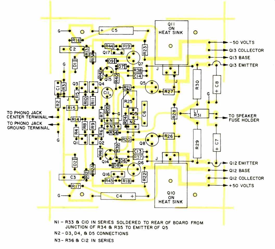
Fig. 3
All components for the VI limiter mount on the printed circuit layout of Fig. 3 except diodes D10 and D11.
These are soldered across the collector-to-emitter terminals on the sockets for transistors Q12 and Q13, respectively. It should be noted that R18 and R19 should be reduced from 390 ohms to 360 ohms when Q16, Q17, R43, and R44 are added to the circuit.
Since the values of R33 and R34 are 30 ohms, the total emitter load resistance of Q6 and Q7 will remain 390 ohms.
Fig. 3-Circuit board parts layout for one channel. View is from ground plane side of the board on which most components are mounted. Note that R33 and C10 are now connected to the rear of the board from the junction of R34 and R35 to the emitter of transistor Q5. This modification is discussed in the text.
A Note on Power
Comments from readers of the first article have shown a great deal of interest in increasing the output power of the amplifier. This can be accomplished easily by using a power transformer which has better regulation than the one specified. A recommended substitute is the Signal transformer number 68-6 or 68-8 which are available from Signal Transformer Co., Inc., 1 Junius Street, Brooklyn, New York 11212. This transformer has multiple primary taps. The tap which produces a d.c. power supply voltage closest to ±50 volts (not to exceed ±52 volts with 120 volts a.c. input line voltage) should be used. The amplifier will then be capable of 100 watts per channel with an 8-ohm load. If any problems are then experienced with either power supply or speaker fuses blowing at high volume levels (especially with 4-ohm loads), the fuses can be changed to ones with a 5-ampere rating. Higher rated fuses should not be used. Under no circumstances should anything but fast blow fuses be used for either the power supply or speaker fuses.
In addition to the transformer change, it is recommended that the Motorola transistors MPS8099 be substituted for Q1 and Q2 and MPS8599 substituted for Q3 and Q4. These transistors have a higher voltage rating than the 2N5210 and 2N5087 which were originally specified. An optional modification for the higher powered unit would be to use four output transistors per channel. By connecting an additional output transistor in parallel with each existing one, the power dissipation per transistor is halved, which improves the reliability of the output stage. The additional output transistors are not necessary if load impedances less than 6 to 8 ohms will not be driven.
PARTS LIST
Original Parts List Modifications
Q1, Q2, Q5, Q17 MPS8099* (or 2N5210)
Q3, Q4, Q16 MPS8599* (or 2N5087)
Q14 2N5681 Q15 2N5679 D3 through D5 1N4004* (or 1N4002)
D6 through D11 1N4004 R1 10 ohm*, 1/4 watt R2 4.7 kilohm*, 1/4 watt R18, R19 360 ohm*, 1/4 watt R28 100 ohm*, 1/2 watt R29, R30 0.33 ohm*, 5 watt
R31 10 ohm*, 2 watt R33 100 ohm, 1/4 watt R36 33 kilohm, 1/4 watt R37, R38 120 ohm, 1/2 watt R39, R40 1.5 kilohm, 1/2 watt R41, R42 33 kilohm, 1/4 watt R43, R44 30 ohm, 1/4 watt C10 10 pF*, 100 volt ceramic capacitor C11 100 µ F*, 10 volt electrolytic capacitor
C14 47 pF, 100 volt ceramic capacitor C15, C16 0.05 microfarad, 25 volt ceramic capacitor
* Indicates a change in value from that originally specified.
The circuit boards for the power amp are available from: William R. Dunn, Georgia Institute of Technology, EES-ASD/STL, Atlanta, GA 30332.
The price is $16.00 per pair, plus $1.00 postage and handling. Note: These boards have provisions for 4 output transistors per channel.
(Source: Audio magazine, Feb. 1977; W. Marshall Leach [*Assistant Professor, School of Electrical Engineering, Georgia Institute of Technology, Atlanta, Georgia 30332 ] )
= = = =