For low-noise measurements, this unit adds three decades of measurement to the bottom end of any high-performance AC voltmeter -- and also features an A-weighting filter.
For making noise measurements in low-noise audio systems, it is desirable to be able to measure micro- volts of noise. This noise meter amplifier (NMA) is designed specifically for the HP 3400A true-RMS voltmeter, but it works just as well (but with more limited bandwidth) with my HP 339A distortion test set and my fluke 8050A true-RMS digital multimeter (DMM). All three meters have a low-end resolution limit of 1mV full-scale (ES).
Another useful feature I added is an “A-weighting” filter, which is a special filter used in sound level and audio noise meters. It is a selective bandpass filter designed to complement the subjective way we hear, because the ear’s sensitivity versus frequency is not flat.
The ANSI A-weighting curve uses a wide bandpass filter centered at 25kHz, with 20dB attenuation at 100Hz, and 10dB attenuation at 20kHz. It provides a steep rolloff for the low end and a more gradual rolloff at higher frequencies. It is the inverse of the 30-phon, or 30dB- sound pressure level (SPL), equal-loudness Fletcher-Munson curve. By contrast, the ANSI C-weighting curve is flatter, with —3dB corners of 31.5Hz and 8kHz, respectively.
The parts list cost in Table 1 is less than $70.
HOW IT WORKS
The schematic diagram for the NMA is shown in Fig. 1. The main power source is two 9V batteries, which must be used in the highest gain ranges if very low noise measurements are going to be successful. S1 is a DPDT center-off switch that can select either the battery power or a supply that rectifies the 12V AC input from a plug-in AC adapter at J5.
When you select battery power, C and C2, in conjunction with ferrite beads FB1 and FB2, low-pass filter any HF noise, while C3 and C4 are the main reservoir caps. C5—Ci0 provide local supply bypass for the three op amps. LED R28, and R29 function as the power-on indicator. In order to minimize power drain on the batteries, I chose an LED that has noticeable brightness at only 0.3mA.
When you select AC power, CR1 and CR2 half-wave rectify the 12V AC into roughly ±18V DC. C28 and C29 provide the primary ripple filtering, which is then applied to reservoir caps C3 and C4 through 1125 and 1126, forming a low- pass filter. 1125 and 1126 utilize the quiescent current of the three op amps to drop the supply to ±15V DC at the op amp rails. I did not use series IC regulators because they did not improve noise over this simple it filter.
The noise amplifier circuit consists of series gain stages U1 and U2. In order to make measurements convenient, the overall gain at the most sensitive range is Av = 1000 (60dB). This allows me to read 1uV FS on the 1mV FS range of the AC voltmeter. S2 allows me to select three gain ranges: 30dB (Av = 31.62), 40dB (Av = 100), and 60dB (Av = 1000). This makes the noise amplifier useful for other types of measurement and amplifying applications.
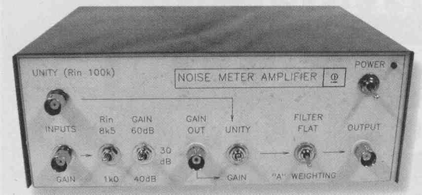
PHOTO 1: FRONT VIEW OF NOISE METER AMPLIFIER
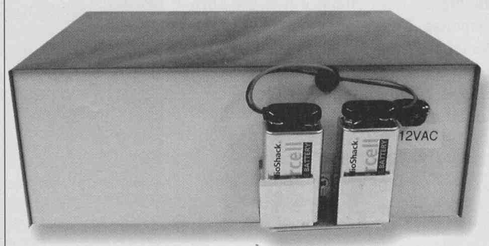
PHOTO 2: REAR VIEW OF NOISE METER AMPLIFIER
The noise amplifier circuitry will generate noise of its own through the input noise voltage and current of the op amps (e and i and the thermal Johnson noise from all its resistors, so be careful when selecting components. I used two low-noise AD745JN op amps that Walt Jung graciously provided from his sample stock. The 8-pin DIP version is available from Rochester Electronics, a source of obsolescent semiconductors (www.rocelec.com). However, you can also use the AD745JR 16-lead SOIC version. Alternatively, you could use the OP-37 low- noise op amp, but there will be a bit higher noise, especially at the higher Rin setting, where the low 6.9fA/’JHz current noise of the AD745 outperforms the OP-37 at 0.4pA/\/Hz.
The AC signal at gain input J2 is coupled by C11 and R3 to U1, making it possible to measure AC noise in the presence of a DC voltage. I used this NMA to measure the AC noise of DC audio supplies in the “DacT CT 102 Power Supply Product Review”. S5 selects between two Bin input impedances: 600-ohm or 8k5. The LF -3dB point for each setting is 56Hz or 4Hz, respectively. The HF bandwidth is 225kHz. I added R1 to discharge C11 when the NMA is not in use.
Since the AD745 is only stable for gains >= 5, Walt suggested placing C12 and C13 (a value four times that of C14) across the inputs. These capacitors, in conjunction with C14, force the noise gain to 5, and provide stability over the entire operating range. I divided the gain equally between the two AD745 stages. During testing, I found that R10 needed to be a bit higher than R5 for exactly 60dB gain, probably due to the variations in the 1% tolerance of all the resistors.
The output of U2 goes through R23 to gain out jack J3 and also to 53. This switch selects between the gain stages of U1, U2, and a unity gain buffer U3B. The common pole of 83 delivers the selected signal to a passive “A-weighting” filter network
I chose this particular filter circuit instead of others published earlier 3 because SPICE simulations showed it to be more accurate to the A-weighting curve U3A adds the necessary gain to recover the losses through the passive network and provide unity gain at 1kHz. S4 selects either the flat response from S3 or the A-weighted response from U3A and drives J4 via R20.
CHASSIS ASSEMBLY
I built the NMA into a painted steel Radio Shack enclosure. The front view is shown in Photo I and the rear view is Photo 2. The two 9V batteries are external to the unit to make replacement easier. Photo 3 is the interior view. The shells of the two input jacks are grounded to the enclosure along with the circuit board ground plane. This re quires that you remove the paint from the enclosure at the points of contact.
In addition, every signal wire that goes to a switch or jack uses shielded cable grounded only at one end to pre vent ground loop noise from being picked up on the signal conductor. The output jacks are isolated from the chassis, again to prevent ground loops. The LED and power supply wires are twisted to minimize pickup or noise radiation.
CIRCUIT BOARD LAYOUT
I built the circuit on a ground plane PC board. This is absolutely necessary at these high gains to ensure the minimum input-to-output noise. Photo 3 shows the view of the PC board, and Fig. 2 shows the parts placement. I used low-profile gold-plated DIP sockets for the three op amps.
The PC board itself was a fairly simple layout, so I routed it with a 0.046” router bit in my Dremel tool rather than use an etched PC board. This maximized the ground plane area. I drilled the board for standard T-49 vector pins so I could tweak any part values later.
Wherever the pins are not to be grounded, I used a Vector P138A pad cutter to cut an electrically isolated circular pad on the copper side around each 0.042” (#58 drill) hole. (The pad cutter is available from Mouser as p/n 574-P138A.) Some parts, such as the power-supply components and de-coupling caps, are soldered directly in place since they would not require changing during testing.
FRONT PANEL
Figure 3 shows the panel lettering designations for the front panel. I made a full-size copy of this lettering on drafting appliqué film, which is an adhesive-backed transparent plastic. The light color base paint on the RS enclosure works well with the black photocopy lettering.
All circuit board mounting holes have clearance for a 4-40 screw with a flat washer. I used four tapped aluminum spacers to mount the board to the chassis.
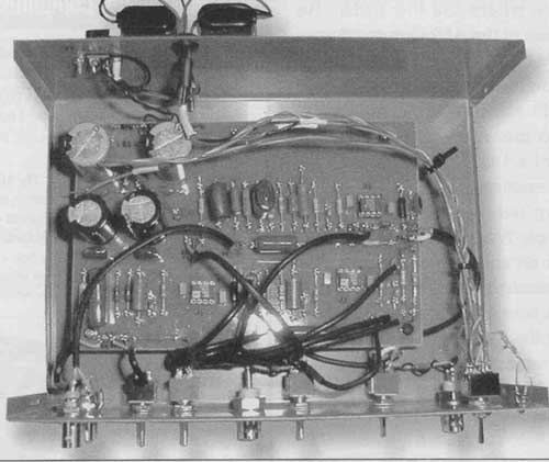
PHOTO 3
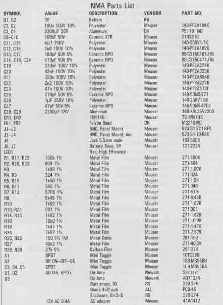
TABLE 1
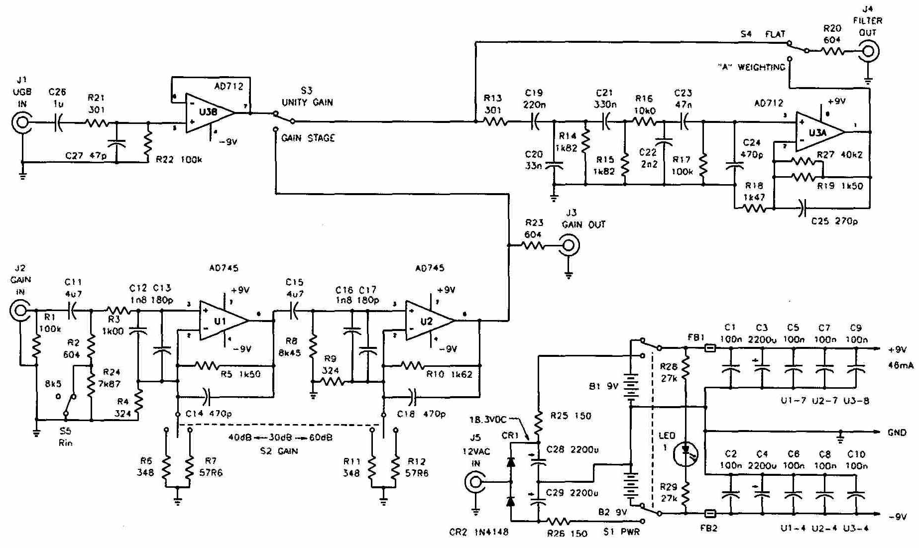
FIGURE 1: NOISE METER AMPLIFIER SCHEMATIC.
MEASUREMENTS
I calculated the ideal noise level for the U and U2 gain stages using an Excel spreadsheet. The total output noise voltage was 12.92uV_/Hz, or 91.4nV RMS over the audio bandwidth. This would be 91.4pV RMS noise referred to the input (RTI) at 60dB gain.
At 60dB gain, the NMA proved to have 3.4mV RMS residual output noise with the input shorted, and 4.7mV RMS with the input open (using the HP 3400A). The noise floor referred to the input (RTI) is 3.4 RMS and 4.7 RMS, respectively. This is the output noise divided by the noise gain of the amplifying circuit (quite a bit higher in the real world than the ideal calculations predict). Table 2 summarizes the measured broadband and A-weighted output residual noise relative to 2V RMS, and the noise referred to the input (RTI), using battery power alone.
Table 3 shows the same data points using the AC adapter supply, which raises the noise floor.
Figure 4 shows the NMA frequency response relative to 2V RMS output. The unity gain input and the gain stage at 8k5 Rin curve are essentially flat. The gain stage with 600-ohm fin has more droop at the low end reflecting the inter action of the lower input resistance with the 4u7 input coupling cap. Note that the gain stage curves have been normalized at 0dB for clarity (the dB gain has been subtracted out). The A-weighting filter response is shown, along with the published curve (dashed line).
Figure 5 shows the THD+N versus frequency for each of the gain settings, and for the unity gain input with and with out the A-weighting filter. The input signal was adjusted in each case for 2V RMS output into a 10k load at 1kHz.
Figure 6 shows the THD+N versus output voltage into a 10k load at 1kHz. The solid lines represent battery power for all gain settings and unity gain with and without the A-weighting filter. The two dashed lines show the THD+N at 40dB gain and unity gain, using the AC power adapter as a source.
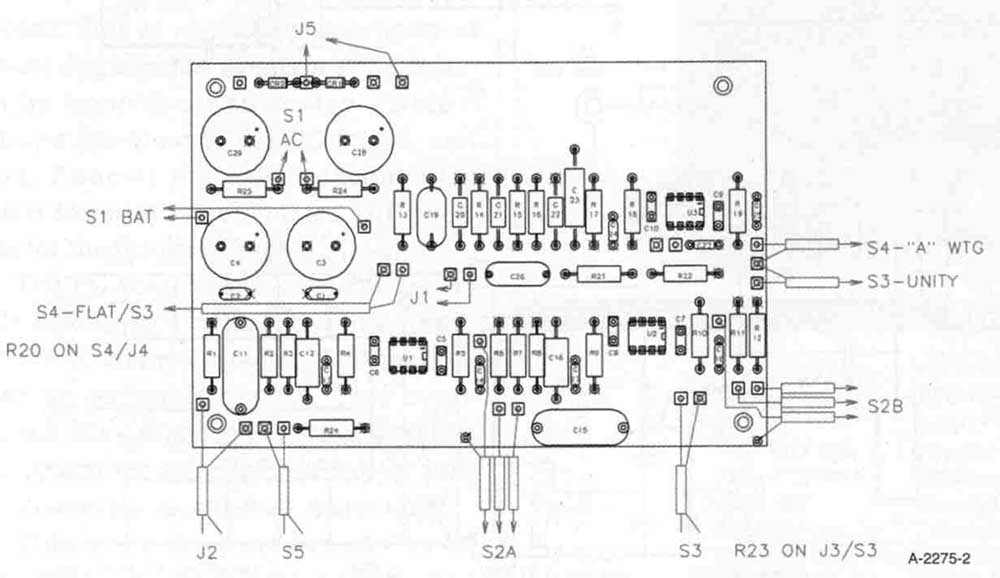
FIGURE 2: CIRCUIT BOARD PARTS PLACEMENT.
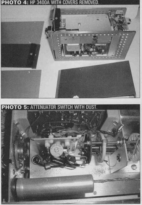
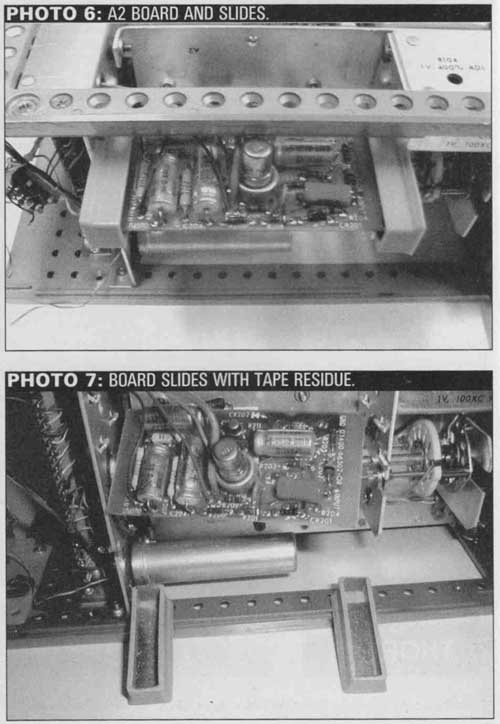
PHOTO 4-7
USING THE NOISE METER AMPLIFIER
You can use the NMA with any standard X1 oscilloscope probe. The output is connected to any broadband AC true-RMS voltmeter with a 1mV RMS full scale. The reading on the meter is then multiplied by the gain used in the NMA.
For low impedance sources such as power-supply noise measurements or for standard 600-ohm pro audio loads, use the 600-ohm R_in position. To measure the noise of higher impedance sources such as preamp line outputs, use the 8k5 Rin position to avoid overloading them; or you can use the unity gain buffer input for driving the A-weighting filter directly without any overall gain. I’ve listed a few more sources of noise measurement information in the References list.
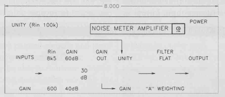
FIGURE 3: FRONT PANEL LETTERING.
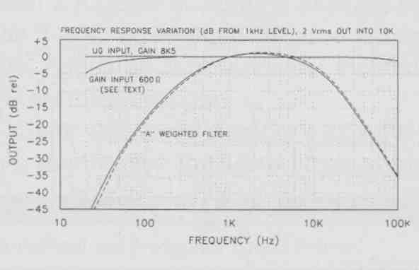
FIGURE 4
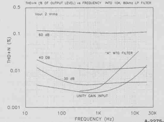
FIGURE 5: NMA THD+N VS. FREQUENCY
The battery power mode with its ±9V rails has less headroom than the AC adapter mode with ±1W rails. Tables 1 and 2 and Fig. 6 show the noise and distortion headroom penalty for using the AC adapter.
THE DESIGN
A block diagram of the HP 3400A is shown in Fig. 7. The meter uses the highly accurate thermocouple method of EMS measurement. The AC input signal is applied to a 10M-ohm input attenuator, which feeds the nuvistor cathode follower impedance converter. The converter drives a second 600-ohm attenuator assembly that is switched in conjunction with the input attenuator to keep the nuvistor output voltage between zero and 100mV full-scale on all ranges.
The second attenuator drives a video amplifier, whose AC output is used to operate the heating element of one section of a sealed dual-thermocouple module. This thermocouple output is input to a modulator and chopper amplifier. The chopper output is demodulated, current amplified by an emitter follower, and drives the front panel analog meter.
Feedback is taken from the emitter follower back to the heating element of the second thermocouple in the module. The two thermocouple outputs are connected in reverse polarity and the closed loop meter circuit nulls the combined series thermocouple output to provide an accurate reading of the AC input signal regardless of its waveform or crest factor. The HP-3400A is accurate to 1% from 50Hz to 1MHz, and has 5% accuracy from 10Hz to 10MHz.
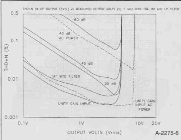
FIGURE 6: NMA THD+N VS. OUTPUT VOLTAGE.
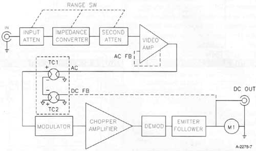
FIGURE 7: HP 3400A VOLTMETER BLOCK DIAGRAM.
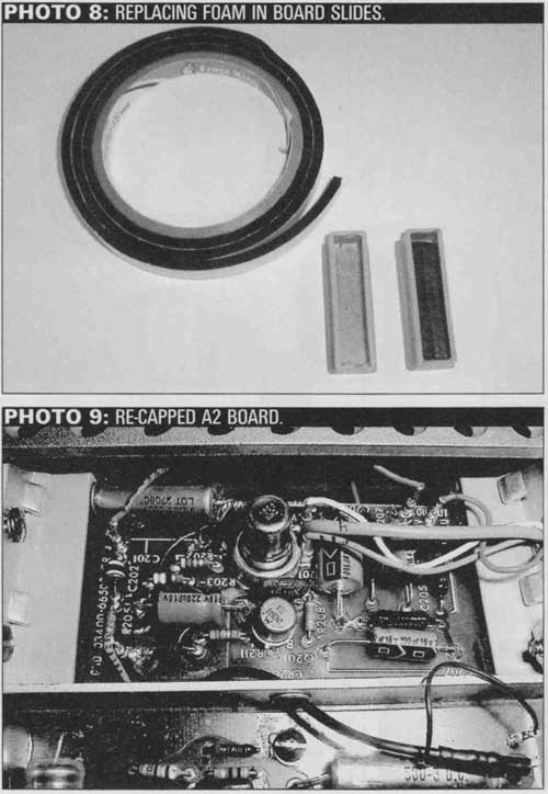
PHOTO 8: REPLACING FOAM IN BOARD SLIDES; PHOTO 9: Re-capped board
If you are selecting a 3400A, try to find one that is not “decorated” with the previous owner’s lab sticker (other than calibration stickers). Ex-government agency and military units are especially likely to have painted stencils and large hard-to-remove stickers on them.
You may be able to renovate a 3400A using just my description and the ac companying photos, but troubleshooting and repairs will require the Operating and Service Manual. There have been a number of running changes to the 3400A throughout its production life. Appendix C in the latest manual covers these changes.
Units with serial number prefix 806- are the newest. Earlier prefixes were 322, 401, 528, and 714. Most of the changes pertained to the chopper amplifier A6 board, the AS photochopper, and the thermocouple pair on A4. I find that even the older units can have very good performance.
One thing I can guarantee is that when you first remove the meter covers, it will be filled with the powdery residue of the deteriorated foam rubber used to shock-mount the A2 nuvistor board. The second most likely problem is lack of a power cord.
====
RENOVATING THE HP 3400A RMS VOLTMETER
The output of the noise meter amplifier must be fed to a wide-bandwidth true-RMS reading AC voltmeter. One such meter that is readily available on ebay and from surplus lest equipment vendors is the Hewlett-Packard 3400A. It cost about $750 new in the 1960s, but clean working units are available on eBay for under $100.
The 3400A is all solid-state except for one RCA 7586 nuvistor triode, used as the impedance converter from the 10M-ohm input attenuator network to the 6000 output attenuator. (The later HP 400E AC voltmeter, not a true-HMS meter. was a descendant of the original HP 400 vacuum tube voltmeter, and uses a JFET impedance converter.) The HP 3400A can read from 1mV RMS to 300V RMS full-scale. The HP 3400A Operating and Ser vice Manual and nuvistor tubes are also still readily available.
=====
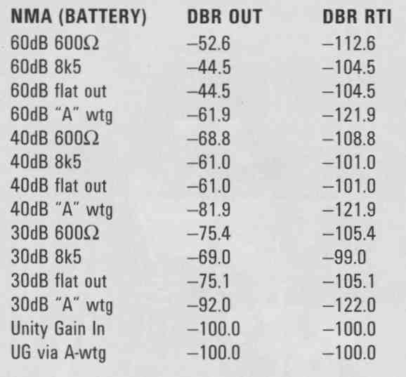
TABLE 2: Broadband and A-weighted Output Residual Noise Relative to 2V RMS, and
the Noise Referred to the Input (R using Battery Power.
TABLE 3: Broadband and A-weighted Output Residual Noise Relative to 2V RMS,
and the Noise Referred to the Input (RTI) using AC Adapter Power.
All-vacuum tube gear such as the HP 400D VTVM had attached power cords. The HP 3400A uses an old-style removable power cord based on the Switchcraft AC3G receptacle. These power cords are very hard to find because HP used them for only a few years in the mid- before the removable IEC cord became standard.
After a fruitless search for an HP power cord, my solution was to convert the meter to a standard JEC power receptacle. I have since renovated a number of 3400As the same way (this power receptacle modification also works for the earliest HP 400E AC voltmeters). The final step in my standard renovation was to replace the meter output signal phone jack with a more useful BNC jack.
GETTING TO WORK
Photo 4 shows the HP 3400A with the top, bottom, and side covers removed. There is a shield that covers the attenuator area in the bottom of the chassis and the nuvistor A2 board. While it looks complicated, it is held in place with one hex nut near the tube cutout and a second hex nut on a captured stud that fits in a slot in the plate with the power transformer mounted to it.
Photo 5 shows the attenuator switch area filled with the powdered foam from the A2 board card mounts. The first order of business is to remove the two plastic PC board holders. The A2 board and the two holders slide out of the chassis from the side. Be sure to guide the top of the nuvistor tube below the bottom left rail as you remove the A2 board to avoid damage.
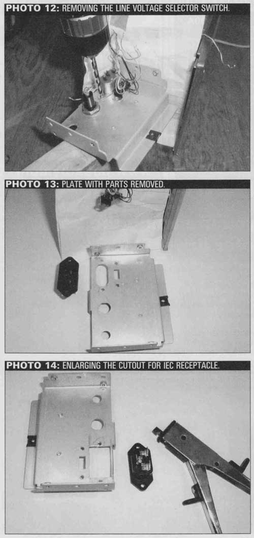
PHOTO 12-14: ENLARGING THE CUTOUT FOR IEC RECEPTACLE
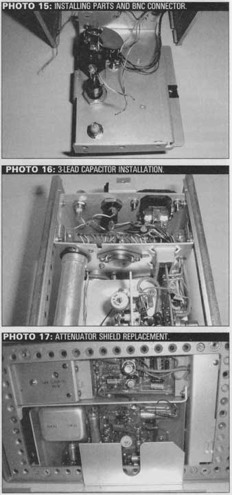
PHOTO 15-17:
Once the two slides are fully extended, you can remove them from the sides of the A2 board. All that will remain of the shock-absorbing foam will be the sticky back tape (Photo 7). Scrape the tape and the foam residue from out of each PC board holder.
Next you are going to replace the erstwhile foam with some 3/8” wide 3/16” thick self-stick high-density weatherproofing foam such as Frost King R338. Cut the replacement foam to length and use a razor knife to slit it down the middle, to within ¼” of each end (not full length, see Photo 8). The slits will center the A2 board when you reassemble the unit. In order to properly hold the A2 board in position, you will need two layers of foam in the right holder to equal the total original foam thickness.
Next, use a soft paintbrush to clean all the foam dust out of the unit. It will have worked its way into every nook and cranny. Use a can of computer dust remover air spray if needed. You may even need to remove the plug-in PC boards to clean their chassis connectors.
Inspect the electrolytic caps on the A2 board. You may choose to re-cap it if they are deteriorated, as I did on one meter (Photo 8). You can easily remove the board by disengaging the push-on terminal wires from their pins. Be sure to make a drawing of the wires and their colors—I recommend you have the manual in hand for this.
REPLACEMENTS
The parts list in Table 4 gives the Mouser part numbers for suitable re placements for all the aluminum caps. The level of capacitor technology in the 1960s was not what it is today. Most of those old aluminum caps had a tolerance of +100%/—10% or worse. Today ±20% is fairly standard. Replacing every aluminum cap is fairly cheap (about $15) but very labor intensive.
For the two large can caps (C1 and C2), you can connect replacement radial lead caps right across the old terminals and leave the original caps in place on the chassis. CE Manufacturing is also making replacement can capacitors for vintage audio gear (info@cedist.com).
If you don’t have the HP power cord, you can easily enlarge the cutout for the original Switchcraft AC3G connector to accept a modern IEC receptacle. Remove the four flathead screws that hold the rear panel connector plate, making sure not to lose the cone-shaped lock washers. Slip the plate out of the chassis (Photo 10). Before removing anything, make a list of the wire colors for each of the following wires (Photo 11).
Unsolder the white/green/gray wire to the phone jack and remove the jack Unsolder the white/brown/gray harness wire to the fuse holder (no need to remove the one to the power socket). Unsolder and remove the 3-wire ceramic capacitor on the back of the power socket. Finally, unsolder the three wires from the socket (white/brown/ gray, white/gray, and black).
The line voltage selector switch is riveted to the back plate and must be drilled out so you can remove the switch from the plate without having to remove all its wires. I used a 13/64” drill (Photo 12). It turned out to be easier to also remove the fuse holder for better access. Be very careful and support the rear plate with care. The wiring used in the 3400A is fragile #24 and #26 and can easily be broken.
Once the switch is removed, the plate is free from the chassis. Now drill out the two rivets holding the AC socket, and the plate will be clean of all components (Photo 13).
Now you must enlarge the AC socket hole to accept the JEC power receptacle. Scribe an accurate horizontal line on the inside of the rear plate exactly 1/16” up from the bottom of the plate. This will be the bottom of the new opening for the IEC receptacle. Next lay out scribe lines for the IEC socket outline, using the outside mounting hole to locate its horizontal position. I used a Radio Shack 64-823A nibbler tool to quickly enlarge the opening in the thin aluminum (Photo 14). Be careful not to bend or damage the thin 1/16” web that is left on the bottom of the opening.
RMS VOLTMETER
I used 6—32 screws to mount the new IEC receptacle. You will need to en large the old outside rivet hole and drill a new hole for the inside screw. Use flat washers under the heads of the screws and lock washers inside, and install the JEC receptacle with its center ground pin at the bottom of the rear plate. Next install the line voltage switch with 4—40 screws, flat washers, and lock washers. Finally, replace the fuse holder and in stall the BNC connector in place of the phone jack (Photo 15).
Now you need to install the 3-lead ceramic cap onto the IEC receptacle terminals, without soldering the leads yet. The cap should point upward from the bottom of the chassis. It must fit between the receptacle and the green connector for the A7 board at the back of the unit. If this cap is damaged, you can replace it with two individual 10nF 250V AC ceramic disc caps.
Next solder the wires you removed earlier back onto the IEC receptacle, the fuse holder, and the BNC jack. Carefully route the wires so they are not pinched between the green connector and the 3-lead capacitor (Photo 16). Replace the four screws that hold the rear panel in place.
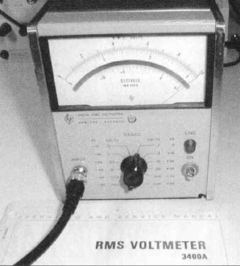
Photo 18
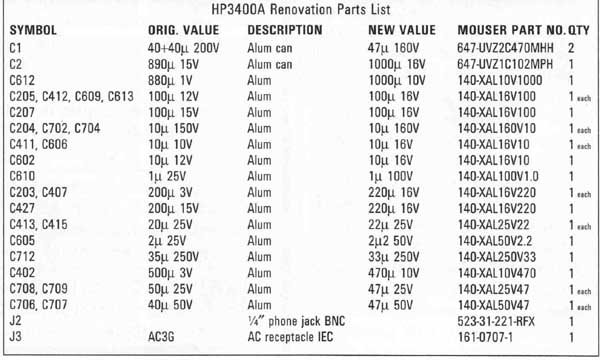
TABLE 4: HP3400A Renovation Parts List
Before replacing the attenuator shield (Photo 17), coat the rotary switch contacts with Caig deoxiT or other good contact cleaner. Photo 18 shows the 3400A alive and well on the calibrator. Calibration is fairly straightforward, but you will need the manual to perform all the steps. De pending on the IEC receptacle you select, you may need to use the nibbler to notch some clearance in the bottom cover where it wraps around and sits against the receptacle flange.
============