Starter Kits, Part 1-- EB-604/410--All-JFET Line Amp
By Erno Borbely
This noted circuit designer begins his starter kit series with an all-JFET line amp.
If you have been following my designs through articles in Audio Amateur publications, you know that my priorities are lowest possible noise, best inherent linearity, and DC coupling. Low noise, of course, is a necessity in this digital age when you are playing CDs with >100dB S/N ratio, but to me a low noise phono preamp and a low-noise microphone preamp are even more important. My interest in inherent linearity stems from my objective of not having to use negative feedback to "clean up" a bad design.
I use feedback primarily to stabilize certain DC or AC parameters of the amps or to achieve special frequency responses, such as in RIAA phono preamps or crossover filters. I use DC coupling whenever possible, because I don't like "capacitor sound" and also because I am "allergic" to the prices of so-called high-end capacitors.
Of course, all of this should always go hand in hand with the overall objective in audio: good sound.
Having said that, I also must admit that these objectives can drive the prices to a level where only a handful of people can afford them. And yes, I do design such "price no object" custom amps for those who have extremely high-resolution systems. However, I would also like people with limited budgets to experience and enjoy my designs. Consequently, I have given up some of the highest design criteria and have come up with designs that are affordable, yet still offer high sound quality, carrying the Borbely Audio sound signature of high resolution and transparency! In this context I designed a series of new kits called Starter kits.
The Starter kits are relatively simple and inexpensive JFET or all-FET circuits. The "secret" of the high-quality sound lies not only in the topologies, but also in the passive components used. I have also included simple discrete all FET regulators for each of the circuits, because I don't want you to use 3-pin LM317/337 type regulators, which are not up to the task required by today's audio amps (see the note on my home page under Upgrades).
These circuits are further developments of the basic ones described in previous articles ("JFETs: The New Frontiers, Part I and II," AE 5/99 and 6/99, and "All-FET Line Amp," aX 5/02.) You'll find copies of these articles on my homepage under Special Articles. Please print out and read these articles because I am going to refer to them frequently in the description of the new ones.
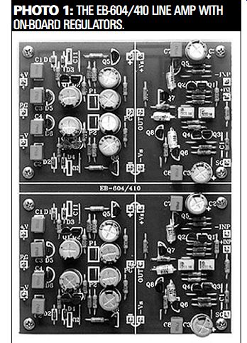
PHOTO 1: THE EB-604/410. LINE AMP WITH ON-BOARD REGULATORS.
DEVELOPING THE NEW TOPOLOGY
The differential amplifier, which was described in Part II of the JFET articles (see Fig. 12A/B, p. 16, in AE 6/99), is the basic building block on which many--if not all--of my amplifiers are based (more on "if not all" in Part II).
I'll give a quick recap of the operation of the differential amplifier here, but you can find a more thorough description in Part II of the JFETs article. Figure 1A shows the basic configuration, which essentially joins two common emitter amplifiers by their sources. You can do this as long as the two JFETs are identical. If the I_0 is constant, then ID1 + ID2 is also constant because ID1 + ID2 = I_0.
----------------
ABOUT THE AUTHOR
Erno Borbely received an MSc degree in Electronic Engineering from the Norwegian Institute of Technology, University of Trondheim. In the 60s he was working as a design engineer for the Norwegian Broadcasting Corp., developing studio equipment, both in tube and in semiconductor technology. In 1969 he moved to the US and worked for David Hafler at Dynaco. Mr. Borbely was named Director of Engineering for Dynaco in 1972. He developed the Cascode output stage for the Stereo 400 power amplifier, and the Dyna tune circuit for the FM5 FM tuner, for which he received a US patent. In the 70s he worked at Motorola Semiconductor, developing power amplifiers, low-noise preamplifiers, and FM tuners. Some of this work was put to good use, when he joined the David Hafler Company in 1978 as Director of Engineering. Mr. Borbely developed the DH101 preamplifier and the DH200 power amplifier, which was the first one to use MOSFETs in the US. From 1980 until 1997 he worked for National Semiconductor in Germany as its Technical Training Manager. In 1984 Mr. Borbely and his wife Irene started Borbely Audio, which sells high quality kits to end-users. Since 1982 he has been publishing his designs in the Audio Amateur publications (Audio Amateur/Audio Electronics, Speaker Builder, Glass Audio, and now in audioXpress). In the last several years Mr. Borbely has developed a line of all-FET audio amplifiers. Besides the kit business, Mr. Borbely is designing audio products for OEM customers. Mr. Borbely's web page address is borbelyaudio.com and his e-mail address is erno@borbelyaudio.com.
-----------------------
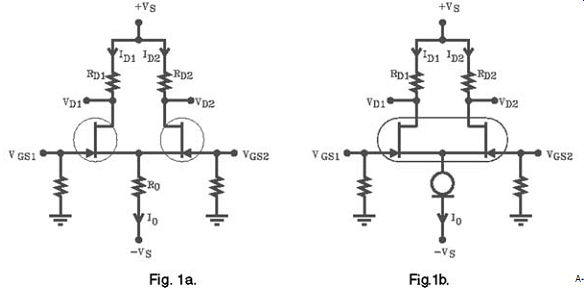
FIGURE 1: THE BASIC DIFFERENTIAL AMPLIFIER.
The prerequisite for this is that R0 is very large. For R0 to be very large -VS must also be very large. This is usually inconvenient, and instead of making R0 large, replace it with a constant-current source as shown in Fig. 1B.
The operation of the differential or balanced amplifier is simple. Holding VGS2 constant and increasing VGS1 will increase ID1. However, ID1 + ID2 = I_0, so if ID1 increases, then ID2 must decrease.
This will cause VD1 to decrease and VD2 to increase for a differential voltage at the output. If you change VGS1 and VGS2 at the same time, but in opposite directions, then you achieve the same effect, but even more of it--i.e., you have more differential gain. This is now a truly differential amplifier with gain of: AV(DD) = (VD1-VD2)/(VGS1-VGS2) Now, what happens if you increase VGS1 and VGS2 in the same direction? If both are going positive, then both drain currents should increase. However, this is impossible, because ID1 + ID2 = I_0. Consequently, the differential amplifier can not amplify same-polarity or common mode signals.
Based on this differential amplifier, I designed a balanced/SE all-JFET line amp, described in Part II of the article (see Fig. 17 on p. 18; also available as a kit under the designation: EB-2000/402, see my homepage). Many customers, including pro audio people, built this amp and called it a "very musical" amplifier.
The only problem I have with this circuit is that the outputs are not sitting at 0V DC and a capacitor is necessary to couple the output to the outside world. I generally don't like caps in the signal path, even if they are made of 99.99% silver.
(I must admit that part of my dislike is caused by the fact that people are charging outrageous prices for the caps.) Fortunately, it's easy to design DC coupled amplifiers because of availability of complementary devices. Figure 2 shows how a common-source amplifier used as a level shift device can turn the differential amplifier into a DC-coupled one.
DC COUPLING
Figure 2A shows the basic circuit. The input JFETs are closely matched and are operated at approximately 2mA each.
The constant-current source that supplies the 4mA is made up of two J508s or two E-202s in parallel. The 2mA drain current in each JFET causes a voltage drop of 3V across each of the 1k5 resistors. This 3V produces about 3.1V across the 332R source resistor of the J74, setting up approximately 9mA in the second stage.
I tried the circuit first with a resistive drain load of 2k49 in the second stage. This resulted in an open loop gain (OLG) of only 27dB. The linearity was also less than adequate with an open loop THD of 0.2% at 3V/1kHz. When I replaced the 2k49 with a 10mA constant current source, the OLG increased to approximately 40dB and the linearity also improved to 0.075% THD at 3V/1kHz.
The drain of the J74 sits at close to zero volts, but a certain offset trimming is necessary. The 50R trimpot serves this purpose. The 10k-1k1 feedback resistors give a closed loop gain (CLG) of 10× (20dB). The closed loop THD at 20dB gain is 0.0045% at 3V/1kHz and 0.02% at 3V/10kHz.
If you operate the amp with a CLG of 6dB, then you need to put a 22pF cap across the feedback resistor. The THD is reduced to 0.0017 and 0.0037%, respectively. The circuit is not unity gain stable (NUGS), but you can force it by dramatically increasing the cap across the feed back resistor to 220pF! Conclusion: don't use it as a unity gain buffer! You can further improve the linearity by converting the common-source second stage to a folded cascode (Fig. 2B). Here the second stage is driven not only by the gate but also by the source.
The second stage then becomes a part of the first stage, coupled to it through the drain resistors.
The 20dB CL THD is 0.0035% at 3V/1kHz and 0.013% at 3V/10kHz. The 6dB figures become < 0.001 and 0.0017, respectively. The high frequencies benefit most from this conversion. The maximum output swing with ±24V supply is about 10V RMS. Minimum load is 10k.
By the way, the amp is still NUGS! You can also use these three-JFET amps in a unity gain inverting configuration. Connect the + input to ground, lift off the 1k1 from ground and use this as the -input. I tried it with 10k-10k for 0.001% THD at 3V/1kHz and 0.0032% at 3V/10kHz. This is a very simple I/V converter for your CD player.
ENTER COMPLEMENTARY SYMMETRY
The three-JFET circuit in Fig. 2B is essentially a simple discrete opamp, with very decent performance. However, in my experience, complementary symmetry improves the neutrality and transparency of the amp. This, I believe, comes
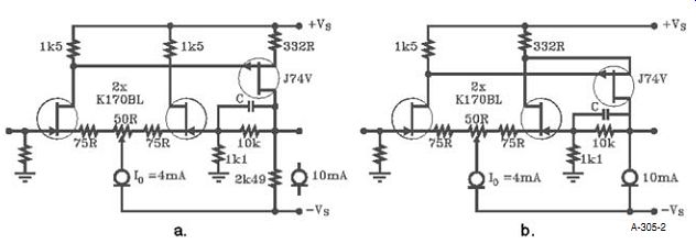
FIGURE 2: A J74 LEVEL-SHIFTER TURNS THE DIFFERENTIAL AMP INTO A DC-COUPLED
AMP.
from further improvement of the inherent linearity, which manifests itself not so much in less measured THD, but in the way the distortion products look, indicating fewer higher frequency components.
I have therefore designed a fully complementary version of the simple amp shown in Fig. 2B (see Fig. 3). Consider the circuit in Fig. 2B as half of a complementary circuit. I have folded this down along the ground line, naturally replacing the n-channel JFETs with p and vice versa.
You can feed the input stages of this new circuit with 4mA constant-current diodes as before, but because the sources of the upper JFETs are sitting at a small but positive voltage and the lower ones at a negative voltage, they can be joined together through a resistor and will feed each other with the necessary source current. A simple trimpot will allow you to adjust this current to the de sired level. An offset adjustment is also necessary as before.
The second-stage JFETs are connected together at their drains, acting as constant-current sources to each other. The whole amp is now a transconductance amplifier, converting input voltage to output current. You convert this output current back to voltage by connecting a resistor from output to ground. Here this resistor is connected back to the negative input of the differential input stage, acting both as a load on the output and a feedback resistor.
With the same feedback networks as before (10k-1k1), the OLG has increased to 300×, which is almost 50dB. The OL THD at 3V went down to 0.06%. The 20dB THD figures are 0.002 and 0.0059%, which are almost 6dB better than the three-JFET circuit.
Interestingly enough, the transconductance amp can drive just about any thing within its current capability, with out much change in the magnitude and structure of the THD. This is an advantage, because a simple load resistor can change the OLG and the OL frequency response of the amplifier without affecting the linearity. Nevertheless, I prefer to isolate the transconductance amp from the outside world with an output buffer, partially to allow low impedance loads, but also to control the OLG independently of the load. This will be helpful in an RIAA phono preamp, as you will see later.
THE EB-604/410 LINE AMP
Based on the transconductance circuit developed in Fig. 3, I designed a complete line amp. The Starter kit EB 604/410 line amp is a high-quality, low noise, low-cost all-JFET circuit, with on board regulators. It is designed to work with 6-20dB gain. For gains up to 12dB, you can use single-matched JFETs (de livered with the kits).
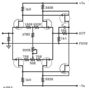
FIGURE 3: THE CIRCUIT CONVERTED TO A FULLY COMPLEMENTARY DIFFERENTIAL CIRCUIT.
For DC stability, I recommend dual monolithic JFETs at 20dB gain. The PCB is 105 × 145mm and contains two completely independent circuits. The amps can be supplied from one common or two independent power supplies. The schematic is shown in Fig. 4.
The input stage is a complementary differential circuit, consisting of Q1-Q4.
Each of these JFETs is working with 2mA drain current. Q1-Q2 (K170BL/ V) and Q3-Q4 (J74BL/V) are closely matched devices. Alternatively, you can use dual monolithic JFETs for Q1-Q2-P1 is setting up the drain current to 2mA and P2 is used to adjust the output offset to 0V. The second stage Q5-Q6 (J74V/K170V) is a folded cascode, coupled to the input stage through resistors R3/R4 and R10/R11. It is using matched high Idss JFETs, and is operating at close to 10mA. John Curl used the same folded cascode configuration in his JC-2 phono preamp module, but he used bipolar transistors for the folded cascode.
The output stage, consisting of Q7-Q8, is a complementary JFET follower circuit (see description in Part II, p. 18, Fig. 16B, of the JFETs article). Again, these are closely matched devices, operating at <9mA, to limit their power dissipation. If you use higher Idss devices, you must put small TO-92 heatsinks on the devices. The circuit is not unity gain stable without the caps C5 and C6 (100pF). At gains >6dB you can reduce the caps to 33pF.
You will recall from the JFET articles that the K170 and J74 JFETs have relatively high input capacitance. Unfortunately, this input capacitance is also voltage dependent, which might cause distortion in certain cases.
This shows up mostly when you drive the circuit from high source impedance.
I checked this for the 410 and found that there is no change up to a source impedance of 5 k-ohm. This is equivalent to a volume control of 20 k-ohm.
If you need higher value volume control, you can use JFETs with lower input capacitance for Q1/Q2 and Q3/Q4.
The high Vp JFETs have significantly lower input capacitance. I have tried the K246BL and J103BL for Q1/Q2 and Q3/Q4, respectively, and they work fine.
All you need to change is the resistor connecting the two sources together.
Since the gate-source voltage is much higher for the high Vp devices, the resistor must be bigger to set up the same drain current as before. For the K246BL/ J103BL it's about 560R, so use a 332R in series with a 500R trimpot. With the K246BBL/J103BL you can use a 100k volume control without any change in distortion.
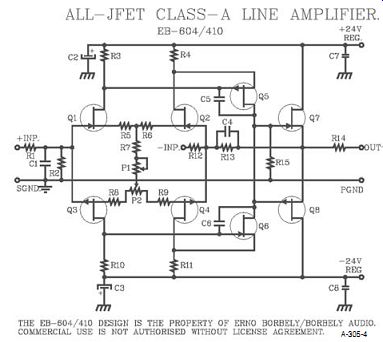
FIGURE 4: EB-604/410 ALL-JFET LINE AMP.
FIGURE 5: EB-604/415 ALL-FET REGULATOR ON THE EB-604/410 BOARD.
---------------
AFTER 20 YEARS, BORBELY AUDIO IS STILL GOING STRONG
This year marks the 20th anniversary of Borbely Audio, and, al though the DIY audio enthusiasts have changed over the years, they continue to be the driving force of our business. Needless to say, our years of experience studying our customers has given us a wealth of information about who they are, why they choose our kits, and what more contributions can Borbely Audio make to the audio market.
To give you a better understanding of how we've determined these, I invite you to view our new online system at www.borbelyaudio.com.
This year Borbely Audio took advantage of technology and transferred all kit documentation, ordering and fulfillment to an online process that enables us to cover and segment our kit offerings from the High-Performance kits, Pro-Audio kits, and our newly released "Starter Kits." Over the past year or so, we've received numerous e-mails, letters, and other correspondence from customers requesting additional kits that are tailored for those beginning their quest for high performance audio.
To that end, Borbely Audio is very proud to release new kits de signed to ensure maximum reliability and performance for the new kit builder. The "Starter Kits" are based on complementary differential designs, exacting superior performance with the same superior components as our other kits share. All of the Starter Kits have on board regulators and newly designed power supplies to complement the kit. We've been able to design these new kits more reasonably priced and yet continue to use the superior components you've come to expect. DIYers everywhere have learned that not all components are made equal.
Our goal as always is to obtain the best possible performance from our components. This is a time-consuming yet worthy task. Components found in many "chain" electronic stores are far inferior in build quality and tolerance. This is one of the single most important aspects for kit builders everywhere. Price is not as strong a factor as you might think with today's DIYers, as we've found price was never a primary issue when exceptional performance was involved. In most cases, price came in fourth behind essentials such as "quality," "avail ability," and "technical support." The new "Starter Kits" provide the best of both price and performance. During the next few months we'll take an in-depth look at these new kits in the pages of audioXpress.
One final observation before turning you loose on the new kits- it's obvious that today's DIY audio kit builders are still around in force. If there is a new design or kit that can be found, they'll find it, simply because they love the experience. The number of online forums for kit builders and DIY audio websites indicates that DIYers are not going anywhere, despite what some might have you believe.
And as long as they are interested in building superior audio equipment, we'll be around to offer it to them.
--Larry Black, Audiokits.com
-----------------
Why not use the K246BL/J103BL in the first place?
The high Vp devices have higher noise than the low Vp ones, and also the inherent linearity is better with the low Vp devices. Nevertheless, the high Vp devices offer a very good compromise between low input capacitance and noise/linearity. I have also tried other high Vp devices, such as the 2N5458 N-channel and the 2N5461 P channel devices, which also work satisfactorily. Don't hesitate to experiment a bit; you have a good chance of getting a very good result.
Only high-quality components are used in the amplifiers. The resistors are non-magnetic DALE CMF-55-143, the electrolytic caps are Nichicon FG-type "Fine Gold" MUSE, and the rest are polypropylene and polystyrene caps. The PCB is FR-4, with the component side printed.
Typical specifications with 6dB gain:
Power consumption per channel: 25mA
Open loop gain: 58dB
Open loop frequency response: 20kHz (-3dB, C5/C6 open)
Closed loop frequency response: >1MHz
Closed Loop THD:
3V/1kHz: 0.0015%
3V/10kHz: 0.0025%
Equiv. shorted input noise: approximately 0.3µV
Input capacitance:
with K170/J74: 45pF
with K246/J103: 7.5pF
with 2N5458/2N5462: 4.5pF
Output impedance: <1 ohm (approximately 50 ohm with R14)
Minimum load: 1 k-ohm
Measured with R12 = 10R, otherwise the noise is dominated by resistor noise.
ON-BOARD REGULATOR
The schematic of the discrete, on-board all-FET regulator is shown in Fig. 5.
The regulators are discrete FET op amps; the positive regulator is made up of differential JFET pair Q1-Q2 (K170BL/V) and MOSFET Q5 (J148), the negative of Q3-Q4 (J74BL/V), and Q6 (K982). Q1-Q2 and Q3-Q4 are closely matched devices. Due to their relatively low breakdown voltage, the maximum input voltage to the regulators is limited to 31V. If the input voltage is >31V the higher-voltage dual JFETs must be used.
The differential pair JFETs are working at 2mA drain current each, which is se up through the 6.9V reference diodes D5 and D6 and source resistors R3 and R4.
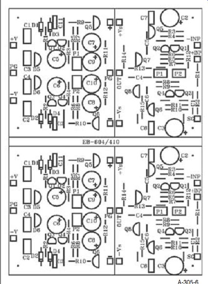
FIGURE 6: STUFFING GUIDE FOR EB-604/410 WITH ON-BOARD REGULATORS.
The reference diodes are fed from constant-current diodes D1 and D2. The output MOSFETs Q5 and Q6 are TO-92 devices and are capable of supplying maximum 35mA. The minimum input output voltage difference is 2V, but I recommend 4V. If the output voltage is fixed at 24V, then adjustment is not necessary and P1 and P2 can be left out (R5 = R6 = 3k32, P1 and P2 are shorted). The output noise of the regulators is <5µV across the audio bandwidth.
Stuffing guide for the EB-604/410 line amp with on-board regulators is shown in Fig. 6. Recommended power supply for the 410/415 combination is the EB 604/263.
SETUP PROCEDURE
If possible, test each amplifier module separately before installing it in the chassis. This simplifies measurements, adjustments, and if necessary, component changes. You need only a basic digital voltmeter (DVM) for the adjustments. However, if you have access to a scope, connect it to the output of the line ...
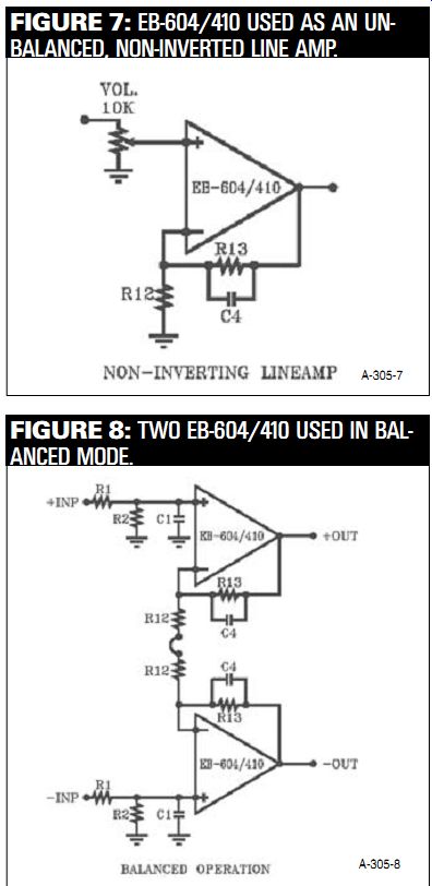
FIGURE 7: EB-604/410 USED AS AN UN BALANCED, NON-INVERTED LINE AMP.
FIGURE 8: TWO EB-604/410 USED IN BALANCED MODE.
FIGURE 9: WIRING DIAGRAM FOR THE EB-604/410 LINE AMP WITH THE EB-604/263 POWER SUPPLY.
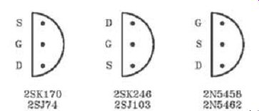
FIGURE 10: PINOUT FOR THE DIFFERENT TYPES OF JFETS (BOTTOM VIEW).
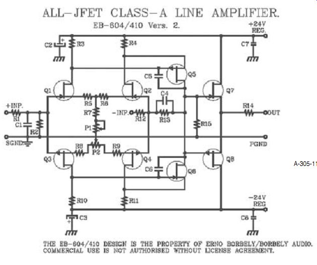
FIGURE 11: THE OUTPUT STAGE IS NOT INCLUDED IN THE GLOBAL FEEDBACK LOOP.
...amp and check whether radio frequency (RF) oscillations are present. If you have complete audio instrumentation in your workshop, perform the usual gain, frequency response, noise, total harmonic distortion (THD), and intermodulation distortion (IM) measurements.
Start the assembly with the regulators.
Insert the solder pins, then add the resistors and the FETs. Finally, install the caps. Connect a 1 k-ohm/1W resistor between the + output and ground and the - output and ground. Connect ±29V unregulated DC to the regulator inputs and check the regulated voltage with the DVM. The output voltage should be ±24V, ±5%.
Next, assemble the amps. Start with the jumpers, then solder the resistors and the JFETs. Finally, add the caps.
Connect the supply jumpers between the regulator and the amp. Connect the +INP of the amps to the input ground. Apply the unregulated supply voltage to the regulators. Check the voltage drop across R4 (or R11) with the DVM. Adjust the voltage drop to 3V with P1. Connect the DVM to the output of the amp and check the offset. Adjust the off set to 0V with P2. The amp is now ready to be installed into the chassis.
APPLICATION NOTES
For 6dB gain connect -INP to ground (R12 = R13 = 2k21). For 3dB gain R12 is 5.6k. If you need 12dB gain, change R12 to 732R or 750R. For a normal, unbalanced, non-inverting line amp, use a 10k or 20k volume control in front of it (Fig. 7). Because of capacitance modulation, I do not recommend volume control higher than 20k, but rather the ALPS 27mm Blue or the 40mm Black potentiometer for volume control.
You can also use two of the EB 604/410s in balanced operation, or as unbalanced-to-balanced converter and balanced-to-unbalanced converter (Fig. 8). For balanced mode, connect the two -INP on the boards together. When used as an unbalanced-to-balanced converter, connect the +INP of the lower amp to ground. For balanced-to-unbalanced operation use the output of the upper amp as the output.
Figure 9 shows the wiring of the line amp. The vertical ground wire on the left-hand side is a bus-bar connecting the ground side of all the RCA connectors together. This is grounded to the chassis, normally on the back panel. You then connect a single insulated wire from this point to the SGND on amp 2. If the power supply is in the same box as the amp then I recommend shielded wire from the RCAs to the input selector switch and from the switch to the inputs.
---------------
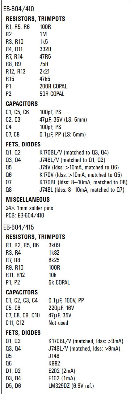
EB-604/410
PARTS LIST
RESISTORS, TRIMPOTS
R1, R5, R6 100R
R2 1M R3, R10 1k5 R4, R11 332R R7, R14 47R5 R8, R9 75R R12, R13 2k21 R15 47k5 P1 200R COPAL P2 50R COPAL CAPACITORS C1, C5, C6 100pF, PS C2, C3 47µF, 35V (LS: 5mm) C4 100pF, PS C7, C8 0.1µF, PP (LS: 5mm) FETS, DIODES Q1, Q2 K170BL/V (matched to Q3, Q4) Q3, Q4 J74BL/V (matched to Q1, Q2) Q5 J74V (Idss: >10mA, matched to Q6) Q6 K170V (Idss: >10mA, matched to Q5) Q7 K170BL (Idss: 8-10mA, matched to Q8) Q8 J74BL (Idss: 8-10mA, matched to Q7) MISCELLANEOUS
24× 1mm solder pins PCB: EB-604/410 EB-604/415
RESISTORS, TRIMPOTS
R1, R2, R5, R6 3k09 R3, R4 1k82 R7, R8 8k25 R9, R10 100R R11, R12 10k P1, P2 5k COPAL CAPACITORS C1, C2, C3, C4 0.1µF, 100V, PP C5, C6 220µF, 16V C7, C8, C9, C10 47µF, 35V C11, C12 Not used FETS, DIODES Q1, Q2 K170BL/V (matched, Idss: >9mA) Q3, Q4 J74BL/V (matched, Idss: >9mA) Q5 J148 Q6 K982 D1, D2 E202 (2mA) D3, D4 E102 (1mA) D5, D6 LM329DZ (6.9V ref.)
-------------------
EXPERIMENTERS AHOY!
Part of my intention in writing this article was to give you a chance to experiment with the circuits yourself. I mentioned that you could use high Vp devices in the input stage, which gives lower input capacitance. I have not tried high Vp devices for the second stage, but you could try some high Idss ones here, too. The K246 and J103 do not come with high enough Idss, so you must find some others.
On the other hand you can use the K246 and the J103 for the complementary source-follower output. Select the highest Idss devices from the "BL" group and match them to ±10% of Idss. You will
lose some inherent linearity using the K246BL/J103BL devices, but they are nevertheless good alternatives for the higher priced K170/J74. Note that the pinout is different for the three types of JFETs (Fig. 10).
Some readers have asked whether you can use the circuit without "global feed back." In this case the global feedback means whether or not the output stage is included in the feedback loop. Figure 11 shows the 410 schematic in which the feedback is taken from the second stage. Compare this circuit with Fig. 3 to see that the input and the second stage are the same as in Fig. 3, with the addition of a complementary source follower stage. Some people believe it should be used this way because the amp sounds softer. I suggest you try it both ways, and choose the configuration that best fits your listening preferences.
The K170BL/J74BL complementary JFET source-follower output stage can drive loads down to 1 k-ohm. Should you need to drive a 600? Sennheiser head phone, you can use two pairs of K170BL/ J74BL in parallel. Some customers have used four pairs of these in parallel to drive 300 ohm headphones! Naturally you can also elevate this design into a higher category by using some of the upgrades I described in the Upgrades notes on the homepage. The Dale CMF-55 143 non-magnetic resistors are very good sounding, but using Cad docks MK-132 instead gives you even more resolution and dynamics. The most dramatic improvement would come from using a stepped attenuator at the input.
Try the fixed-series/variable shunt attenuator (Fig. 9), and you are getting close to my high-performance kits.
AUDIOKITS.COM. 36 Applebee Farms Dr. , Jacksonville, Il. 62650. (217) 243-1006 ; (217) 245-5694 (Fax). 1-888-863-3482 (Toll-free). sales@audiokits.com www.audiokits.com SOURCES ACKNOWLEDGEMENTS My sincere thanks to Walt Jung, who kindly read the manuscript and provided valuable comments and suggestions.
Also thanks to North American distributor Audiokits.com for their continued support and help in the Starter kits development program NOTE ON INTELLECTUAL PROPERTY RIGHTS
DIY amateurs may build this circuit for their own use; however, commercial use or duplication in any form is not authorized. Many of my published circuits have been copied without my permission--not just in the Far East, but also by reputable European and US companies and used in commercial products. This is against the international intellectual property rights.
--------------
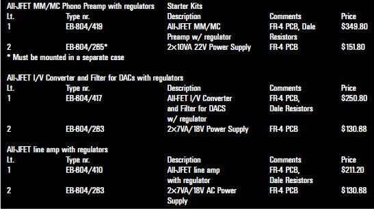
All-JFET MM/MC Phono Preamp with regulators; Starter Kits; Lt. Type nr. Description Comments Price 1 EB-804/419 All-JFET MM/MC FR-4 PCB, Dale $349.80
Preamp w/ regulator Resistors 2 EB-604/265* 2×10VA 22V Power Supply FR-4 PCB $151.80
* Must be mounted in a separate case
All-JFET I/V Converter and Filter for DACs with regulators Lt. Type nr. Description Comments Price
1 EB-604/417
All-FET I/V Converter FR-4 PCB, $250.80
and Filter for DACS Dale Resistors
w/ regulator 2 EB-604/263 2×7VA/18V Power Supply FR-4 PCB $130.68 All-JFET line amp with regulators
Lt. Type nr. Description Comments Price
1 EB-604/410 All-JFET line amp FR-4 PCB, $211.20
with regulator Dale Resistors 2 EB-604/263 2×7VA/18V AC Power FR-4 PCB $130.68
Supply
-------------------------------
============
Also see: