|
|
This low-cost diff amp has good precision and allows you to accurately measure different signals in the presence of high common-mode voltages, such as those you might find in tube equipment or bridged tied output power amplifiers.
An oscilloscope is a very handy tool in audio work, and a differential plug-in allows you to view waveforms that are not referenced to ground. The 7A22 plug-in for my Tek 7603 can work at common-mode voltages as high as ±1000V; or when used at a more modest common-mode voltage of ±1V, it can make differential measurements down to 10 A high-quality differential amp is fairly costly—about several hundred dollars on eBay.
You can build this more modest high voltage differential amplifier (HV diff amp) for about $60. It is based on the Analog Devices AD629 instrument amp IC. This is a monolithic difference amplifier with a high input common-mode voltage range. The AD629 will operate over a ±270V common-mode voltage range, and its inputs are protected from common-mode or differential voltage transients up to ±500V.
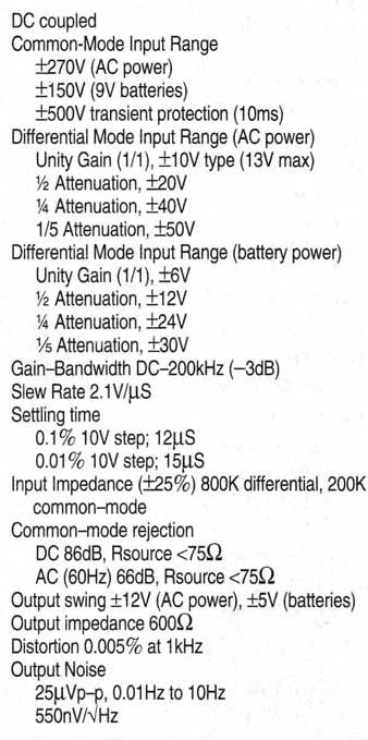
Specifications for the prototype unit are shown in Table 1. The parts list is in Table 2.
HOW IT WORKS
The schematic diagram for the HV diff amp is shown in Fig. 1. The main power source is an 18V AC plug-in AC adapter, or optional power by two 9V batteries. Battery power will reduce the common and differential input range, but allows portability if that is a requirement.
S2 is a DPDT center-off switch that can select either the battery power or the 18V AC input from the plug-in AC adapter at J4. When you select battery power, C5 and C6, in conjunction with ferrite beads FB1and FB2, low-pass filter any HF noise, while C7 and C8 are the main reservoir caps. C9—C12 provide local supply bypass for U1 and U2. LED1, R6, and R7 function as the power-on indicator.
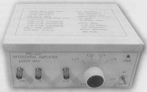
PHOTO 1: Front view of high voltage differential amplifier.
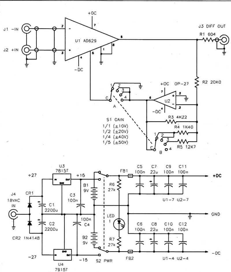
FIGURE 1: HV duff amp schematic.
In order to minimize power drain on the batteries, I chose an LED that has noticeable brightness at only 0.3mA.
When you select AC power, CR1 and CR2 half-wave rectify the 18V AC into roughly ±25V DC. C1 and C2 are the main reservoir caps, and U3 and U4 are linear regulator ICs that provide ±15V DC at the supply rails for U1 and U2. C3 and C4 ensure stability for the regulators.
The AD629 does most of the work, since it has 380k resistors in series with each input lead. The differential gain is Av = 1 (0dB). Differential input signals are applied to U1 through J1 and J2. The ground-referenced differential output is coupled to J3 via current-limiting resistor R1, which also sets the output impedance at about 600 ohm.
The differential input voltage is ±13V maximum for ±15V supply rails, and proportionally less when operating on 9V batteries. There are instances when you may prefer to trade gain for a wider differential input range. I came across a method for doing this in a Burr-Brown applications note (Application Bulletin AB-001) for the INA117 difference amplifier IC, which is an earlier implementation of a high-voltage in amp. The AD629 is pin-compatible with the INA117.
Precision op amp U2 inverts a fraction of the output signal by means of R2 and one of the resistors selected by S1 (R3, R4, or R5). The inverted voltage is fed back to U1 REF+ pin 5, which reduces the gain of U1 in proportion to the resistor ratios. In the unity gain position (1/1), pin 5 is grounded to return to the “data sheet” configuration.
S1 can select from unity gain (±10V nominal differential range, ±13V maximum) to ½ gain with a ±50V nominal differential range (±65V maximum). The INA117 is limited in its gain reduction capability because it is unstable for gains less than 0.2 (1/5). I assume that this same limit applies to the AD629. An added ad vantage of the increased differential range is that the output noise is reduced by the same factor. The common-mode reduction ratio (CMRR) is preserved regardless of the gain reduction.
The DIP version of the AD629 is no longer listed in the latest Newark Electronics catalog. You may be able to obtain it from Analog Devices directly (www.analog.com), or use the SOIC version. The DIP version of the INA117 is available from DigiKey, but observe the reduced common mode and differential input ranges as compared with the AD629.
CHASSIS ASSEMBLY
I built the HV cliff amp into an aluminum enclosure. The front view is shown in Photo 1.1 put a label on the top of the box showing the input and output operating limits, for easy reference.
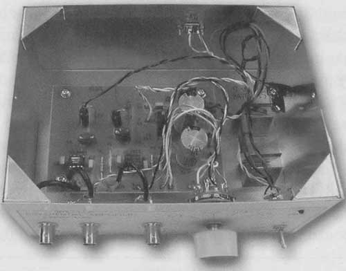
PHOTO 2: Interior view and PCB.
Photo 2 shows the interior view of the HV duff amp. The shells of the BNC jacks are grounded to the circuit board ground plane. The LED and power- supply wires are twisted to minimize pickup or noise radiation. The two battery holders are on the right side of the chassis, with their battery clips.
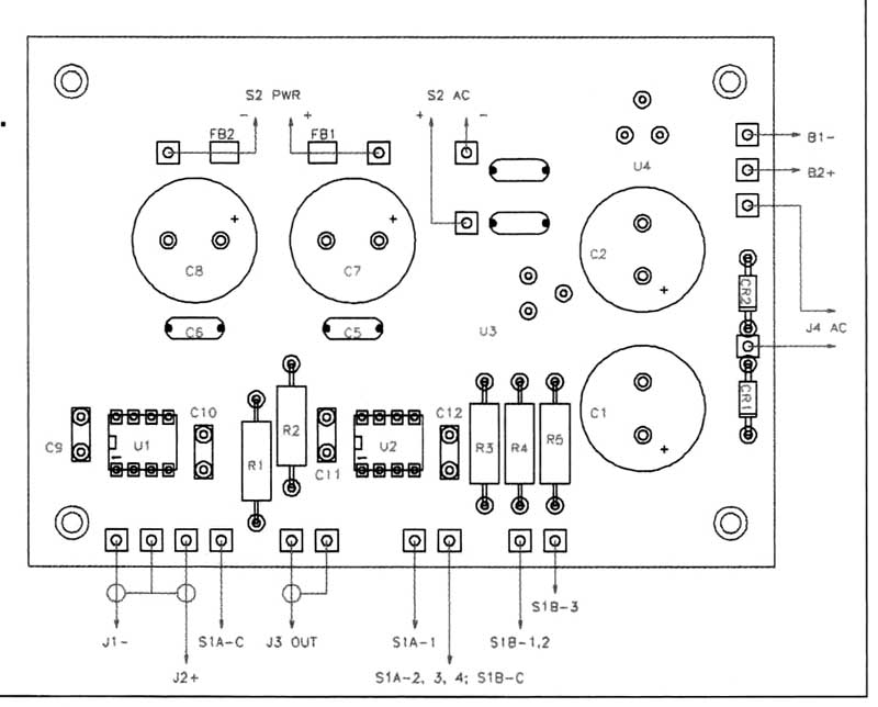
FIGURE 2: Circuit board parts placement.
CIRCUIT BOARD LAYOUT
I built the circuit on a ground plane PC board. Photo 2 shows the finished PC board, and Fig. 2 shows the parts placement. I used low-profile gold-plated 8-pin sockets for the DIP ICs.
The PC board itself was a fairly simple layout, so I routed it with a 0.046” router bit in my Dremel tool rather than use an etched PC board. This maximized the ground plane area. A few in stances required that I wire by hand between components.
Figure 3 shows the top and front view of the chassis with key dimensions, with the panel lettering designations for the front panel. I made a full-size copy of this lettering on drafting appliqué film, which is an adhesive-backed transparent plastic. A coat of light color paint on the enclosure works well with the black photocopy lettering.
The circuit board mounting holes have clearance for a 4-40 screw with flat washer. I used four tapped spacers to mount the board to the chassis. The labels for the top and front panels of the enclosure are shown in Fig. 4.
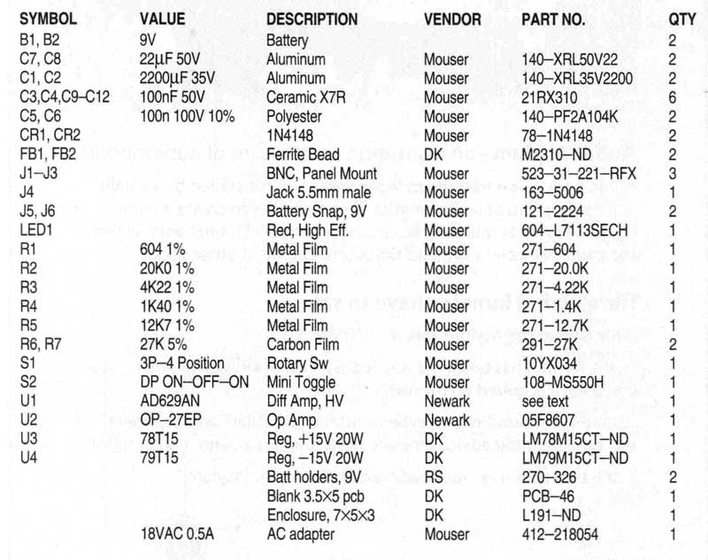
TABLE 2: HV DIFFERENTIAL AMP PARTS LIST
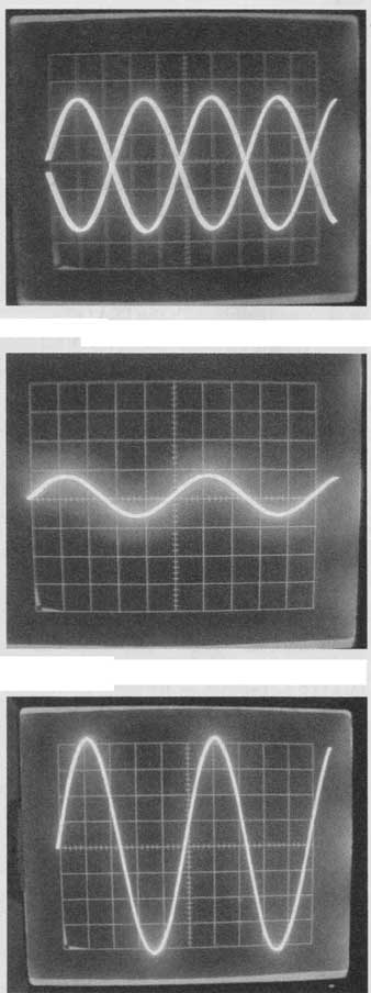
(top to bottom) PHOTO 3: Grid signals from tube phase inverter. PHOTO 4: Plate
voltage using 10x probe. PHOTO 5: Differential voltage plate— cathode using
HV diff amp.
USING THE HV DIFFERENTIAL AMPLIFIER
Signals applied to input jacks J1 and J2 should use standard Xi oscilloscope probes, and the probe end ground leads should be connected together and kept from coming in contact with any ground. The probe grounds will provide signal shielding by way of the HV diff amp chassis.
You can connect the output jack to any high impedance scope or volt meter input by BNC terminated coax. When you select any of the reduced gain settings, you must multiply the scope or voltmeter readings by the inverse of the gain reduction. If you read 5V at the 1/5 gain setting, the actual differential voltage is 25V.
Be sure to keep the common-mode voltage limits in mind when making measurements. High voltages do not appear on the chassis of the HV diff amp, so safety is not an issue as it would be if you used an AC cheater plug to “float the scope” in order to make measurements not referenced to ground. This is a very dangerous practice because it places the entire chassis of the scope at the common-mode voltage level where the measurement is being made (the plate of a tube, for instance).
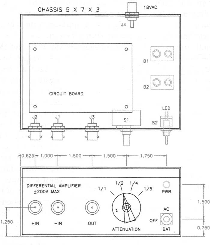
FIGURE 3: Differential amp chassis.
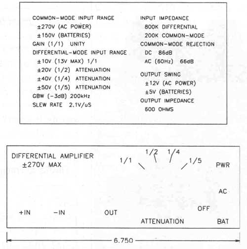
FIGURE 4: Label designations for chassis.
In order to check the performance of the HV diff amp, I bread-boarded the input section of a push-pull tube amplifier. I connected a 12AX7 as a direct-coupled split-load phase inverter. I coupled the plate and cathode through 470nF caps to grounded 470k resistors to simulate the grids of the output tubes. Photo 3 shows the two-channel scope photo of the equal and opposite “grid” signals across the two 470k resistors.
18V RMS, but they are loaded down by the 1M-ohm scope inputs. This is a factor you must keep in mind when working with high impedance circuits. Note that this HV diff amp has an even lower input impedance than a scope, so calculation of the amount of attenuation based on parallel impedances may be necessary in high impedance circuits.
Photo 4 shows the phase inverter plate voltage referenced to ground using a 10x scope probe. The AC signal is riding on the nominal DC plate voltage as it swings between 230V and 282V. This AC component represents the voltage that is coupled to one of the output tube grids.
Photo 5 shows the waveform of the plate-cathode voltage at the phase inverter using the HV diff amp. I set the gain to ½. The output of the HV diff amp is ground referenced, so you can do what you wish with it. You could get a similar presentation on
The voltages are the scope using the 10x probe with AC coupling, or with a differential amplifier plug-in.
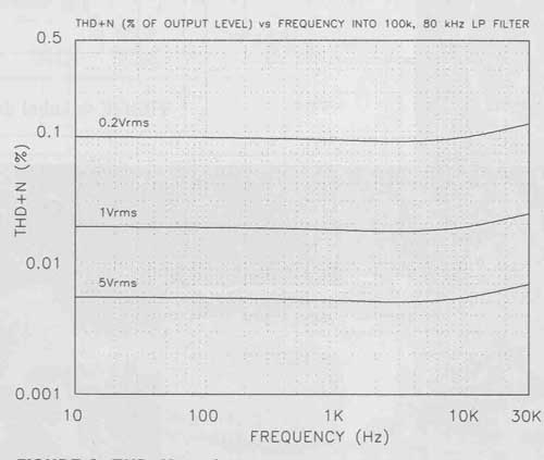
FIGURE 6: THD+N vs. frequency.
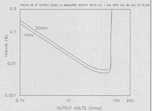
FIGURE 7: THD+N vs. output voltage.
However, the signal from the HV cliff amp can be sent to a distortion analyzer or other low voltage instrument without concern for the high voltage present in the tube circuitry. I measured a THD-I-N of 0.45% across the 12AX7. This fairly high level is probably due to the open- loop connection of the 12 circuitry, and would improve in a close-loop power amplifier.
You might think you could use two 10x probes to increase the common- mode voltage even further. However, this will probably seriously degrade the CMRR of the AD629, whose internal resistors can vary as much as 25% from the nominal values. Refer to AB-001 for details concerning the accuracy and CMRR degradation due to external components.
MEASUREMENTS
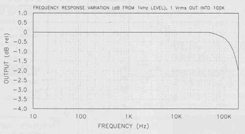
Figure 5 shows the frequency response of the HV duff amp at the unity gain (1/1) setting, from 10Hz to 200kHz. It is ruler flat from DC out to 50kHz, making it very useful for audio work.
Figure 6 shows the THD+N versus frequency for three differential voltages, again at the unity gain setting. The input-referred noise is limited by the Johnson noise of the 380k input resistors in the chip. I engaged the distortion test set 80kHz LP filter to limit out-of-band noise.
The THD+N versus output voltage at unity gain is shown in Fig. 7. The THD is a bit higher at 20kHz due to the usual gain-bandwidth limitations.
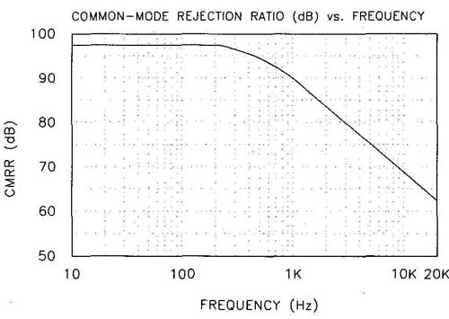
Finally, Fig. 8 shows the common-mode rejection versus frequency. Even at 20kHz, there is 65dB CMRR available. This requires that both inputs be at the same impedance, as low as possible to prevent CMRR degradation.
============
