In Part 2 the author explains the hardware implementation of the Virtual
Crossover.
By RM
In Part 1 [coming soon], I explained the motivation and theory behind the Virtual Crossover, a device that can either temporarily or permanently re place the real crossover circuit in a speaker system. In a temporary application, you can use it to optimize the component values for the real crossover that will eventually replace it; however, if you use it in place of a real crossover, it allows you greater freedom to do things that are not possible with either passive or active real circuits.
Before I proceed to discuss my implementation, I should mention that I decided to build this as a stand-alone device that can operate independently of a PC, although it can also interface to a PC through the RS-232 serial port. I'm sure it is also possible to implement it using some kind of plug-in card in a PC, but I chose not to do this for several reasons.
First, the plug-in cards that I thought might have the capabilities I required were either very expensive, or it was not clear to me how to write specialized software for them. Second, the idea of trying to carry out a real-time simulation using Windows was a bit daunting.
Finally, since I ultimately intended to use this device to play music, I preferred not to start up a PC every time I wished to play my stereo. Nevertheless, I'm sure a PC design would also be a valid approach for this device, and if you should develop such a design, I would be very interested to hear about the results.
IMPLEMENTING THE BASICS
Because it will be important to the discussion of the components in the Virtual Crossover, I repeat the following equation from Part 1: (9) Equation 9 shows how to calculate the output of the crossover, Vout (n), at time n delta_t, given an audio input, Va and the impulse response of the crossover circuit, h_imp. The equation is just a discrete form of the convolution integral, and it is also the expression for the output of a class of digital filters called FIR (finite impulse response) filters.
The most basic requirement for the Virtual Crossover is to perform the above calculation efficiently. Actually, you must calculate equation 9 more than once within each time interval: for each crossover filter and for both left and right- channel audio signals, resulting, for example, in four separate calculations for a two-way speaker system.
The logical choice to implement this calculation is one of the available DSP (digital signal processing) chips. These chips are specifically optimized to carry out the type of calculation in equation 9, which can be described as a series of "multiply-accumulate" steps. I chose the ADSP21061 chip made by Analog Devices, which can perform a complete multiply-accumulate step in a single processor cycle. In fact, it can do more than that; it can multiply--accumulate and fetch new values from a calculation buffer in a single cycle.
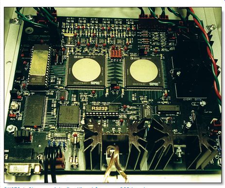
PHOTO 1: Close-up of the first Virtual Crossover DSP board prototype.
This is also a floating-point chip, which is necessary to calculate equation 9 accurately for a wide range of audio in puts. The clock speed for the device I am using is 40MHz, so that a multiply- accumulate cycle is carried out in 25ns.
The 21061 chip is available in a surface mount package, but it is a difficult one-there are 240 pins, with lead spacing of about a quarter of a millimeter.
Hand-soldering a device with such a fine lead spacing is nearly impossible, or at least extremely difficult. I had never designed a surface-mount board before, so the prospect of using such a package was intimidating.
However, in checking with a local PCB fabrication company (Hughes Electronics in Livonia, Mich.), I discovered that the usual procedure is to have such fine-pitch ICs mounted by a ma chine at the time the board is fabricated. That was encouraging, but the down side is that in order to place the solder paste used for the surface-mount ICs, a stencil is required that adds a couple of hundred dollars to the start-up costs of the board.
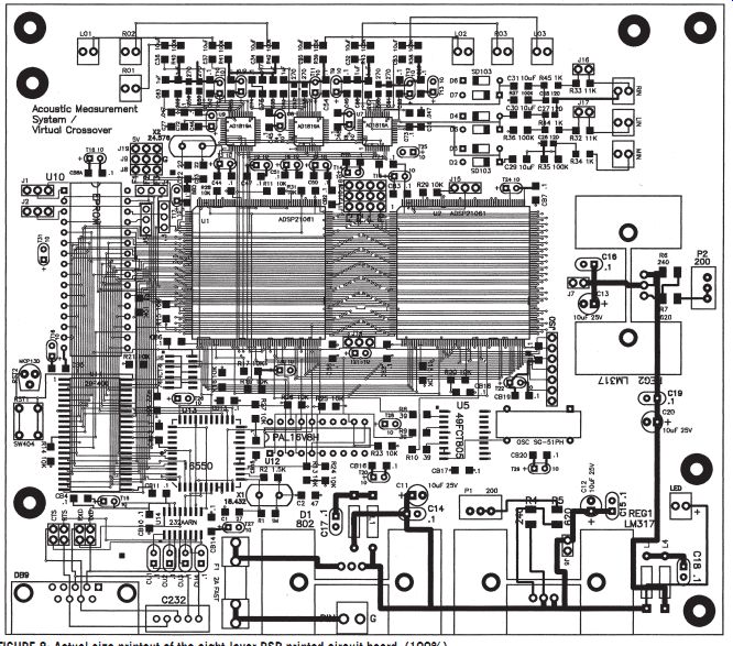
FIGURE 8: Actual size printout of the eight-layer DSP printed circuit
board. (100%)
A MULTILAYER PCB
I ended up designing a multilayer printed circuit board (Fig. 8) for this project, with eight layers (including those on top and bottom) and with surface mount components on top of the board.
To design it, I used an excellent soft ware tool called Tango PCB, made by Accel Technologies. I used version 1.07 for DOS, which I purchased several years ago and which I don't believe is available anymore; however, Accel Technologies offers more recent versions of this product for Windows.
I can't really recommend trying to fabricate this board as a DIY project un less you have a lot of experience with such designs; instead, if you are thinking of building this device, I would recommend obtaining a fabricated board from me, with at least the ICs already mounted. You can solder the discrete components by hand if you wish, although even that requires patience and a steady hand.
In addition to carrying out the equation 9 calculation, the other basic requirement for the Virtual Crossover is the capability of sampling analog audio signals, converting the results to digital form, sending the samples to the DSP for processing, and converting the processed results back into analog form to drive the speakers. To perform all these functions, I chose Analog Devices' AD1819A SoundPort Codec, which packs quite a bit of audio processing in a small package.
The AD1819A carries out all the functions I've listed, including band-limiting of the audio signal with both analog and digital filters. It is intended to inter face with a DSP controller such as the ADSP21061, communicating with it through the synchronous serial port, using a protocol referred to as AC-Link.
This protocol sets up a continuous, bidirectional flow of serial information between the DSP controller and the Codec, with each complete transfer occurring at a standard 48kHz sampling rate. In each 48kHz sampling interval, the Codec sends to the DSP the most re cent values it has sampled from the audio inputs, and the DSP simultaneously returns the most recent values it has processed (according to equation 9) that are ready to be applied to the speakers.
The AD1819A uses a 16-bit A/D converter to discretize the audio input signal. It also has digitally controlled input and output gains, which you can select in steps of 1.5dB.
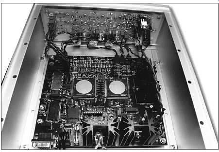
PHOTO 2: View showing DSP board and Output board mounted on front panel.
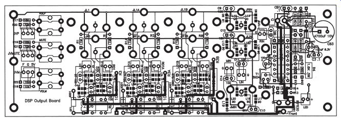
FIGURE 9: Printout of the two-layer Output printed circuit board. (90%)
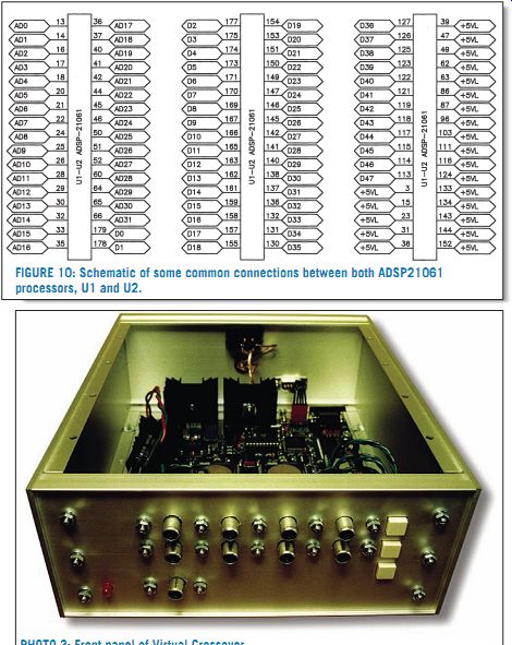
FIGURE 10: Schematic of some common connections between both ADSP21061
processors, U1 and U2.
PHOTO 3: Front panel of Virtual Crossover.
POWER AMPLIFIERS
I should mention at this point that between the output of the Virtual Crossover and the speakers, power amplifiers are required; in fact, you need a separate stereo power amplifier for each driver in the system, so that two power amps are necessary, for example, for a two-way speaker such as the hybrid ESL/TL system.
This requirement has motivated me to become involved with power-amplifier design.
One of the reasons I decided to use the AD1819A Codec and ADSP21061 DSP is that a lot of information about these parts is available on the Analog Devices website at www.analog.com, including design examples. As a novice in this area, it was important that I gain sufficient design information if there was to be any hope that my board would actually work. Unfortunately, there is not as much information on the AD1819A Codec as I would like, but there was enough for me to get my very first board working.
In analyzing the impulse responses of some of the crossover circuits I in tended to use for my hybrid ESL/TL speakers, the first intended application for this device, I concluded that I would need to process in the range of 500-600 points per channel within each 48kHz sampling interval, or a total of up to 1200 operations of the type in equation 9.
Since the clock speed for the version of the ADSP21061 I used is 40MHz, this would require a processing time of 30µs, which is greater than the 48kHz sampling interval of 20.83µs. Therefore, I decided it would be necessary to use at least two ADSP21061 chips in parallel to carry out the required calculations. Fortunately, these devices are de signed to be easily connected together, and examples of multiple-chip systems are shown in the documentation avail able from the Analog Devices website. I ended up using two of these devices in my first implementation of the Virtual Crossover.
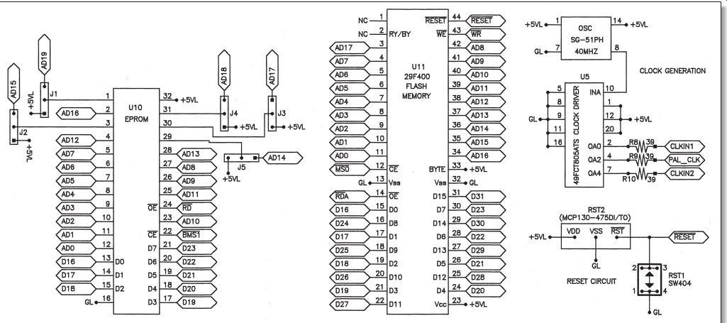
FIGURE 11: EPROM and FLASH memory connections, together with the clock
signal-generation and reset circuits.
The AD1819A Codec provides a single stereo pair of outputs, but this is not sufficient for the multiple drivers of a speaker system. Each impulse-response calculation of the type in equation 9 is for a particular driver; for example, one calculation using the left channel audio input is for the left-hand transmission line in my speaker system, and a separate calculation using another impulse response is for the left electrostatic driver. Therefore, I chose to cascade three AD1819A chips, which is sufficient to supply a three way stereo speaker system. Again, it was fortunate that these devices are de signed to be easily combined, and multichip designs for the AD1819A Codec are also available on the Analog De vices website.
PERIPHERAL CONSIDERATIONS
In addition to the chips that will carry out the basic functions required by the Virtual Crossover, several peripheral features are required. I will describe these systems briefly in this section, then present further details with the schematics.
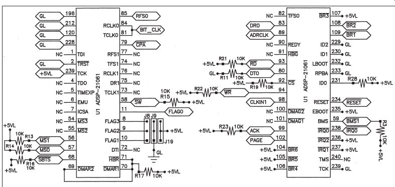
FIGURE 12: Various connections for the master ADSP21061 processor, U1.
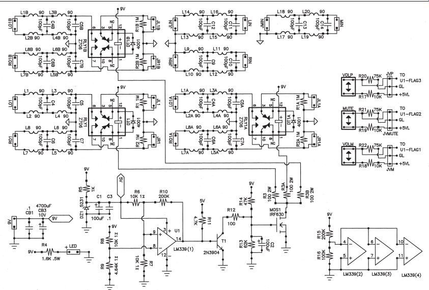
FIGURE 13: Schematic for the Output board mounted inside the front panel
of the enclosure.
The most obvious and important sup port you must add is some sort of memory. The ADSP21061 contains 1MBit of internal SRAM memory, but this disappears when the power goes off; there fore, it is necessary to provide an EPROM chip that boots up the ADSP21061 chips and loads the Virtual Crossover program at startup. I de signed my board to permit using sever al different EPROMs by including selectable jumpers. The EPROM I used initially is the 27C801, which provides 8Mbits, which is more than enough memory for this application.
In addition, considering how the Virtual Crossover will typically be used reveals another type of memory requirement. I envisioned first interfacing the device with a PC through the serial port.
During this stage, I would download to the DSP and try out many different crossover circuit impulse responses. I would also carry out acoustic measurements during this stage to determine the effects of changes in the crossover.
However, once I had determined an optimum crossover design, I wished to download and store the impulse-response information semi-permanently in the Virtual Crossover memory so that, for example, I could power up the device without a PC and have it use the crossover circuit information to play music. To implement this type of operation, some kind of erasable and re programmable memory is required. I chose to use a FLASH memory chip, the AM29F400 by AMD, which provides 4Mbits of programmable memory.
Another important peripheral aspect of this system is the serial interface with a PC, requiring the usual UART and RS 232 level shifter, but additional consideration is also necessary. In order to interface the ADSP21061 with the 16550 UART chip that I used, it is necessary to insert a buffer chip between the two; simply adding wait states to the ADSP21061 memory read/write cycles is not sufficient, because control signals in proper sequence must also be sup plied to the UART. I first became aware of this problem from the ADSP-2106x.
SHARC EZ-KIT
Lite Reference Manual by Analog De vices, where I saw a solution using a GAL16V8 programmable chip as the interface between the ADSP21061 and UART. I developed a similar program for the GAL16V8 and used it in my board design. For the design details, including the .JED file that you can use to program the GAL16V8, please visit my website.
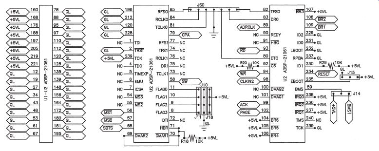
FIGURE 14: Additional common power connections for U1 and U2, together
with various connections specific to slave DSP U2.
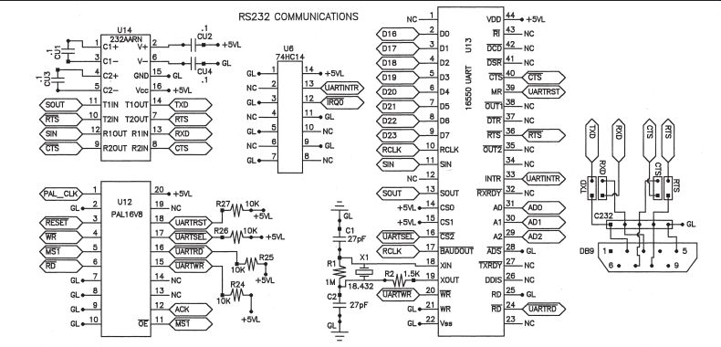
FIGURE 15: Circuits for the RS232 serial interface with a PC.
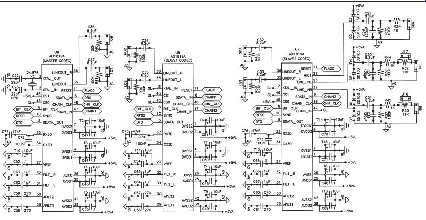
FIGURE 16: Connections for the three Analog Devices AD1819A SoundPort
Codecs.
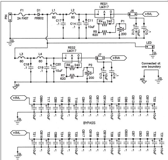
FIGURE 17: Digital and analog power-supply circuits for the DSP board.
THE OUTPUT BOARD
I first made a single PCB for this project, which I referred to as the DSP board.
However, when I tested it I discovered that the audio outputs of the AD1819A Codecs go through a rather nasty transient when they are powered up or reset.
If the Codec outputs are connected directly to power-amplifier inputs, as I envisioned they would normally be, the resulting transient from the power amps might destroy speakers unless the power amps included a timed relay-protection circuit at power-up.
Even if the power amps were protected with relays, a sudden dip in power to the crossover might cause the processors and Codecs to reset, initiating a transient while the power amps were connected. It became evident, there fore, that I needed to include adequate relay protection in the Virtual Crossover itself to avoid such mishaps.
In addition, when it came time to think about placing the crossover in an enclosure and interfacing the three in puts and six outputs to the outside world, it became clear that I needed to design a second board, which I called the Output board, that would include phono jacks for the front panel as well as relay protection.
Photo 1 shows a close-up of the first DSP board that was completed. The output board is mounted on the inside of the front panel of the enclosure; Photo 2 is a view showing both the DSP and output boards. I used PC-mount phono jacks from Switchcraft (no. 3514PC) so that I could mount them directly on the Output board. Photo 3 shows the front panel; the phono jacks and LED are directly soldered in the OUTPUT board. I haven't attempted to label the front panel yet, but I should because it is difficult to remember where all the phono jacks are connected.
I should mention that the schematics do not correspond exactly to the boards shown in these photos. Based on my experience with this first prototype, I have decided on some changes I will make with future boards. I have included these changes in the schematics, since they will be improvements in the Virtual Crossover.
Figure 8 shows an actual-size print out of the DSP board, with the changes that I mentioned already implemented.
Keep in mind that this printout shows all the metallization layers, and since the figure is a single color, it is not possible to tell which lines are on which layers. Figure 9 shows a printout of the Output board, which is a two-layer board with no internal layers.
-----------------------
-----------------------
SCHEMATIC DETAILS
In this section I present detailed schematics of both the DSP and Output boards. With each one, I will discuss important aspects of the design that pertain thereto.
Figure 10 shows some common connections between the two ADSP21061 processors; the notation "U1-U2" indicates that identical connections are made for both processors, U1 and U2.
The labels in boxes indicate common connections that may appear elsewhere on other schematics. For example, "AD0" is the lowest-order bit on the ad dress bus; Fig. 10 indicates that this line is connected both to U1 pin 13 and U2 pin 13. However, this same line will appear elsewhere in the schematics; for example, in Fig. 11 it is also attached to the EPROM and FLASH memory chips.
The common-address and data bus connections in Fig. 10 are necessary to connect the two processors in parallel.
Analog Devices provides information and examples of multiprocessor systems on its website. (These are not the only lines the processors must share; others will appear on later schematics.) In addition to address and data bus connections, Fig. 10 also shows various required power connections for the processors (+5VL, where "L" refers to Logic, as opposed to Analog, power).
Figure 12 shows some connections for the master DSP processor, U1 ("GL" in these diagrams refers to Logic Ground, and "NC" denotes No Connection). MS0 and MS1 lines are used to select external memory, and they must be connected together between U1 and U2; MS0 selects FLASH memory, and MS1 selects the UART. BMS1 is used to select "Boot Memory," which in this case is the EPROM chip U10. Note that many of these lines need to be pulled up.
Several lines in Fig. 12 are involved with the serial interface between the master DSP processor and the Codecs.
This interface follows a protocol referred to as "AC-Link," which provides a method of continuously transferring data and commands at a standard 48kHz rate. BIT_CLK is a 12.288MHz clock that is generated by the master AD1819A Codec, U9, as the timing for this interface. Each information-ex change at the 48kHz rate is initiated by a synchronization signal, RFS0, which is generated by the master DSP, U1.
During each information exchange interval, data is transmitted from the master DSP to the Codecs via the DT0 line, and data is simultaneously sent from the Codecs to the DSP processor on the DR0 line.
In the application information for interfacing the AD1819A Codec to a DSP controller, Analog Devices recommends pulling down the DT0 line with a resistor in the 10-20k range. When I first assembled the DSP board, I used a 15k resistor, which did not work- the AD1819A Codecs did not function properly (Analog Devices explains that they can enter "factory test mode" unless DT0 is pulled down). In order to get the Codecs to work, I needed to use a 10k resistor, which is shown as R11 in Fig. 12.
FOUR FLAGS
Each ADSP21061 processor has four flags that you can configure either as inputs or outputs. I used FLAG0 of DSP processor U1 as an output to reset all three Codecs. The remaining flags, FLAG1-3, I configured as inputs and brought out to header J8. These flags I used as inputs for the volume up/down and mute controls from the Output board, which are push-button switches.
You can see these controls in Fig. 13, the Output-board schematic, and in Photo 3 on the front panel. The adjacent power and ground connections on headers J19 and J9 were also required for these Output-board controls.
RD, WR, and ACK are important signals for interfacing the DSPs to each other and to peripheral devices, and you can find these signals in several locations in the schematics. IRQ0 is the interrupt line to the master DSP processor from the UART (after going through inverting buffer U6), which indicates that the UART has received a byte of information from a PC over the RS-232 serial port. (It is not necessary to have a PC on the serial port for the Virtual Crossover to function, however, if there is no PC, all it can do is play music, using the information that has been stored previously in the FLASH memory.) BMS1 is the boot-memory select line, which selects the boot-up source when the DSPs are powered up or reset. You can see in Fig. 11 that this line selects the EPROM chip, U10. ID0-2 are used to identify master and slave DSPs in a multiple-processor environment; they are set to select U1 as the master, and U2 as the slave.
Figure 14 shows some power connections common to processors U1 and U2, together with some connections specific to slave DSP processor U2. For U2, all four flags are brought out to header J11, even though these flags are not currently used. The flags are very valuable tools in the debugging stage of DSP program development, so they should all be made available even if they will not be used during normal operation of the device.
The lines associated with serial port 0 of U2 are brought to header JS0 in order to accept direct digital input from a CD player, rather than having to sample the input through the A/D converter. I have not yet attempted to do this; it remains as a future project.
The BMS and EBOOT lines control the boot-up sequence when the DSP is powered up or reset. Since I was not sure of the best method to boot up the devices, I brought these lines from U2 out to jumpers J14 and J15 so I could change the settings if there were problems. I ended up setting EBOOT high for both processors and connecting their BMS pins, which means that both devices boot up from the same EPROM at startup. The boot loader provided with the Analog Devices evaluation kit allows each processor to boot a different program from the same EPROM, which is necessary since the master functions somewhat differently than the slave DSP.
EPROM CONNECTIONS
Figure 11 shows the connections for the U10 EPROM, which stores the pro grams that the U1 and U2 DSPs load at startup, along with the connections for the FLASH memory, which stores the impulse-response information and other data that allows the Virtual Crossover to function without a PC. Of course, you must first program the EPROM; I used the Chipmaster 2000 programmer available from Logical De vices, the same programmer that I used to program the PAL16V8 chip for the RS-232 communications interface.
If you are interested in seeing the pro grams I used for the DSPs, I will make the source code available on my web site; these programs, written in assembly code, are called DSPMSTR.ASM for the master ADSP21061 (U1), and DSP SLAVE.ASM for the slave ADSP21061 (U2). I provided jumpers for the U10 EPROM so that you could use different EPROMS. As I indicated previously, the 27C801 device I am currently using has much more memory than is really needed.
Also shown in Fig. 11 is the clock generation circuit for the DSPs and the PAL16V8. The clock signal is one of the most important on the board, and Ana log Devices recommends using a clock driver chip together with series resistors to attenuate reflections on the clock lines. It also recommends laying out the clock lines to reach the devices at approximately equal distances from the clock driver, so that all the devices in the system are synchronized.
Finally, Fig. 11 also shows the RESET-signal generation circuit. I used a "microcontroller supervisor" chip, the MCP130-475DI/TO, which generates a reset pulse whenever the voltage drops below a certain value; this chip is guaranteed to reset somewhere in the range 4.5V to 4.75V. Also, since this device has an open drain output with pull-up resistor, you can connect a reset switch (RST1 in the figure) to manually reset the board.
(One word of caution: if you use this board, do not manually reset it while it is connected to live power amps connected to speakers; if you do, the relays that I mentioned earlier will afford absolutely no protection from the reset transient.)
SERIAL INTERFACE WITH A PC
Figure 15 shows the connections that implement the RS-232 serial interface with a PC. As explained previously, the PAL16V8 chip acts as a buffer between the DSP and UART, allowing signals to be presented in the required sequence and timing. U12 must be programmed, and the program I used (RS232.JED) is available on my website. U6 is an inverter, required only because the 16550 UART generates a positive polarity interrupt signal, whereas the U1 DSP re quires a low IRQ0 interrupt signal.
U14 is an RS-232 level shifter that translates the TTL-level signals from the UART to the approximately ±10V required on the serial line. I provided jumpers at the RS-232 interface output so that, for example, you could also use a null-modem cable. There are two RS 232 output connectors mounted on the board, a header C232 and a 9-pin DB9 connector; I included the DB9 so that you could test the board with a PC while it is removed from the enclosure.
On the back panel of the enclosure, there is also a DB9 connector that would normally be used with a PC; wires from this panel-mount connector plug into header C232.
Figure 16 shows the schematic for the three AD1819A Codecs on the DSP board. These Codecs are connected together in a master-slave type of configuration, with U9 being the master, U8 the slave1 and U7 slave2. Analog Devices provides information on its website about how to interface multiple Codecs, both among themselves and to a con trolling DSP. I needed three Codecs be cause each one has only a single stereo output, whereas I require three stereo outputs for a three-way stereo speaker system.
There are three inputs to the Codecs; LIN and RIN would typically be used for a stereo music input signal, for example, from a CD player. Note that I included with these inputs two 11k series resistors, R32 and R33, which you can optionally short out with jumpers J17 and J16. The input impedance of the AD1819A is specified as 10k in the data sheet, and the maximum input voltage that this device can accept be fore clipping is specified as 1V RMS, or 1.414V peak.
Since the analog output of a CD player can typically be up to 3V peak, it could not be connected directly to the AD1819A input. However, with R32 and R33 in the circuit, together with the 1k-ohm and 100k resistors already there, 3V peak input is lowered to 1.29V at the input to the AD1819A. I included jumpers in case you use a lower-level input source, and this extra attenuation is not needed.
The remaining input, MIN, might be used for a microphone or any other input that requires amplification. MIN provides an optional 20dB gain that you can select or de-select through soft ware. I intended that the MIN input would probably only be used for acoustic measurements.
CODEC FUNCTIONING
The overall function of the Codecs is as follows. Each one is responsible for the output of the left- and right-channel signals associated with one of three crossover circuits. For example, the master Codec, U9, outputs the left and right channels for the first crossover filter at outputs LO1 and RO1. This filter might be the low-pass circuit for the woofers, for example. Slave1 (Codec U8) handles the outputs for the second crossover filter, and slave2 (Codec U7) handles the third filter. In addition, the slave2 Codec is responsible for sampling the audio input signals through its A/D converters and sending the resulting samples to the DSP U1 for processing.
The details of this information exchange may be found in the AD1819A data sheet and other literature available on the Analog Devices website.
The Virtual Crossover can also operate as a measurement system, in which case test signals (typically filtered pulses) are output by the Codecs, and the response (from a microphone, for example, after a specified delay) is relayed back to the DSP for transmission to a PC over the RS-232 port.
Figure 17 shows the circuits for both the digital and analog +5V power sup plies. Analog Devices recommends using separate power supplies if possible, with the grounds connected at one point or in one localized region to avoid ground loops. I used LM317 adjustable voltage regulators for both supplies. Especially for the digital supply, it is important to provide a hefty heatsink and ventilation through the top of the enclosure. I included jumpers at the power supply outputs, J6 and J7, so that I could adjust the supplies before applying power to the rest of the board.
The power input, PIN, is from a 9V DC wall transformer obtained from Jameco. Protection is provided through fuse F1 (this board draws approximately 1.1A when operating normally), and diode D1 protects against accidental application of reverse-polarity power. Ferrites L1-L4 and capacitors C14, C17, C18, and C19 form low-pass filters to isolate digital noise generated on the board from the input power.
RELAY PROTECTION
Figure 13, the Output board schematic, was primarily designed to provide relay protection against the reset transient from the Codecs. It also provides filtering for the input and output signals, isolating them from digital noise generated on the DSP board. Finally, the volume and mute controls are also implemented on this board.
The relay protection works as follows.
Comparator LM339(1) controls whether or not the relays are energized. A 2.5V signal is present at the positive input of the comparator, which is compared to a divided-down 9V power signal from the wall transformer at the negative input.
At power-up, regardless of the state of the output of this comparator, it takes a few seconds for capacitor C2 to charge up to the point that MOSFET MOS1 turns on to switch the relays so the Codec outputs are connected.
Under normal operation, the divided down 9V signal at the negative input would be about 2.85V, so the output of the comparator would be grounded, T1 would be off, and MOS1 would be on. If the 9V power input drops below 7.88V, the output of the comparator goes high.
As a result, T1 switches on, quickly draining the charge from C2 through 100 ohm resistor R12, which turns off MOS1 and disconnects the Codec outputs.
Zener diode DZ1 provides 5V power for the comparator; this 5V is held steady during power transients by capacitor C1.
The series Ls and shunt Cs in the input and output signal paths in Fig. 13 filter out digital noise generated on the DSP board. PC-mount phono jacks are soldered directly to the Output board and protrude through the front panel. A power-indication LED is also soldered directly to the board and protrudes through the front panel.
ENCLOSURE
I used an enclosure available from Lansing Instrument Corp. in Ithaca, N.Y.; the part number for the standard enclosure is B2H10-001A. However, it is desirable to have the top panel perforated at least in the areas above the DSP chips and the +5VL regulator heatsink.
Lansing will punch perforations in the top panel of this enclosure for a very reasonable charge, although there is a $60 additional setup fee for each custom part order.
The standard enclosure itself is $69.71, and the fee for punching the top panel (according to instructions that I supplied to Lansing) is $12.53. Lansing assigned custom-part numbers to this modified enclosure: B2H10-7895 for the complete enclosure with modified top panel, and 38946-7896 for the perforated top panel itself.
I attempted to machine the front and back panels of this enclosure myself; Fig. 18 shows the templates that I used.
As you can tell from Photo 3, my machining capability is rather primitive. I ended up needing to do a lot of filing to get everything to fit in the openings.
COST AND AVAILABILITY
As you have probably already surmised, this is not an inexpensive project. The first prototype DSP board cost $658, including a one-time fee of $270 for the stencil used to mount some of the more difficult surface-mount components.
This cost is for the board itself; it does not include any of the components mounted on the board, although there is a labor charge included to mount some of the surface-mount components when the board is fabricated.
The most expensive component on the board is the ADSP21061 DSP processor, which is about $75 in small quantities, and there are two of them on the board. The initial Output-boards I had made were about $93 each. If you are interested in this system, I may make these boards available at a price considerably lower than that of the initial prototypes, the reduction depending on how many people are interested. If you think you might want to use these boards, please contact me at my e-mail address so that I can give you an idea of what the quantities and prices will be.
In Part 3 I will show how you can use the Virtual Crossover to design the crossover for a hybrid electrostatic/ transmission line speaker system similar to that described in the excellent series of articles by Roger Sanders. I hope to demonstrate some of the unique capabilities of this device that cannot be accomplished with either conventional active or passive real crossovers.
ACKNOWLEDGMENTS
I would like to thank R.J. Smith and Tom Bewick of Hughes Electronics in Livonia, Mich., whose expert and very patient guidance prevented my first surface-mount PCB project from becoming a disaster.
REFERENCES
1. Sanders, Roger R., "An Electrostatic Speaker System-Parts I, II, and III," SB 2/80, 3/80, and 4/80.
RESOURCES
I have posted the software used in the development of the Virtual Crossover. Questions regarding the software or these articles can be directed to my e-mail address at rkm@usol.com.
PARTS SOURCES
Digi-Key Corporation
701 Brooks Ave. South Thief River Falls, MN 56701-0677 1-800-344-4539
Digi-Key.com
Jameco Electronic Components
1355 Shoreway Rd.
Belmont, CA 94002-4100; 1-800-831-4242;
jameco.com
Lansing Instrument Corp.
705 Willow Ave.
Ithaca, NY 14850 1-800-847-3535
www.plantfloor.com/ny/lansinginstrumentcorp.htm
Future Active 1-800-655-0006
www.future-active.com
Accel Technologies, Inc.
12348 High Bluff Dr.
San Diego, CA 92130
www.acceltech.com
Logical Devices, Inc.
2062 Stout St.
Denver, CO 80205 303-308-9600
www.logicaldevices.com
===========
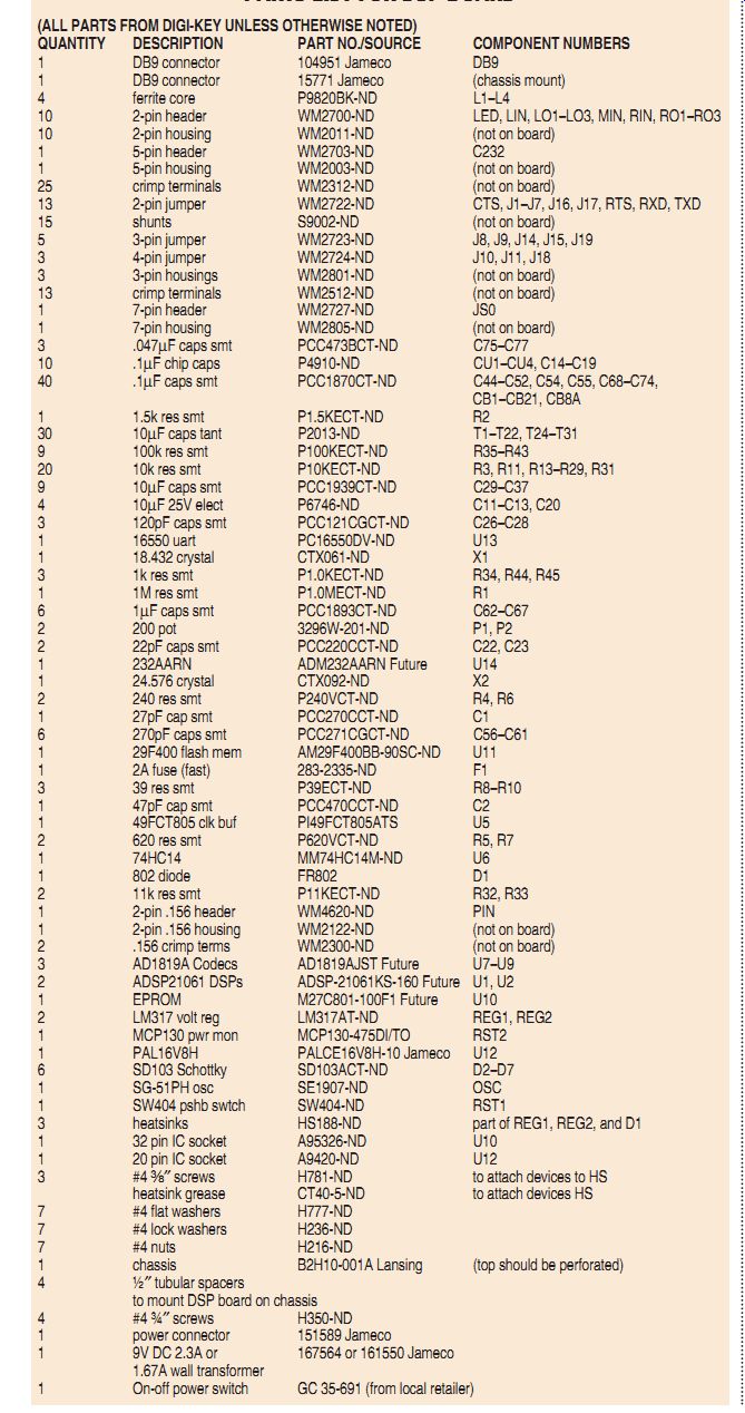
TABLE 1 PARTS LIST FOR DSP BOARD (ALL PARTS FROM DIGI-KEY UNLESS OTHERWISE NOTED)
QUANTITY DESCRIPTION PART NO./SOURCE COMPONENT NUMBERS
1 DB9 connector 104951 Jameco DB9 1 DB9 connector 15771 Jameco (chassis mount) 4 ferrite core P9820BK-ND L1-L4 10 2-pin header WM2700-ND LED, LIN, LO1-LO3, MIN, RIN, RO1-RO3 10 2-pin housing WM2011-ND (not on board) 1 5-pin header WM2703-ND C232 1 5-pin housing WM2003-ND (not on board) 25 crimp terminals WM2312-ND (not on board) 13 2-pin jumper WM2722-ND CTS, J1-J7, J16, J17, RTS, RXD, TXD 15 shunts S9002-ND (not on board) 5 3-pin jumper WM2723-ND J8, J9, J14, J15, J19 3 4-pin jumper WM2724-ND J10, J11, J18 3 3-pin housings WM2801-ND (not on board) 13 crimp terminals WM2512-ND (not on board) 1 7-pin header WM2727-ND JS0 1 7-pin housing WM2805-ND (not on board) 3 .047µF caps smt PCC473BCT-ND C75-C77 10 .1µF chip caps P4910-ND CU1-CU4, C14-C19 40 .1µF caps smt PCC1870CT-ND C44-C52, C54, C55, C68-C74, CB1-CB21, CB8A 1 1.5k res smt P1.5KECT-ND R2 30 10µF caps tant P2013-ND T1-T22, T24-T31 9 100k res smt P100KECT-ND R35-R43 20 10k res smt P10KECT-ND R3, R11, R13-R29, R31 910µF caps smt PCC1939CT-ND C29-C37 410µF 25V elect P6746-ND C11-C13, C20 3 120pF caps smt PCC121CGCT-ND C26-C28 1 16550 uart PC16550DV-ND U13 1 18.432 crystal CTX061-ND X1 3 1k res smt P1.0KECT-ND R34, R44, R45 1 1M res smt P1.0MECT-ND R1 61µF caps smt PCC1893CT-ND C62-C67 2 200 pot 3296W-201-ND P1, P2 2 22pF caps smt PCC220CCT-ND C22, C23 1 232AARN ADM232AARN Future U14 1 24.576 crystal CTX092-ND X2 2 240 res smt P240VCT-ND R4, R6 1 27pF cap smt PCC270CCT-ND C1 6 270pF caps smt PCC271CGCT-ND C56-C61 1 29F400 flash mem AM29F400BB-90SC-ND U11 1 2A fuse (fast) 283-2335-ND F1 3 39 res smt P39ECT-ND R8-R10 1 47pF cap smt PCC470CCT-ND C2 1 49FCT805 clk buf PI49FCT805ATS U5 2 620 res smt P620VCT-ND R5, R7 1 74HC14 MM74HC14M-ND U6 1 802 diode FR802 D1 2 11k res smt P11KECT-ND R32, R33 1 2-pin .156 header WM4620-ND PIN 1 2-pin .156 housing WM2122-ND (not on board) 2 .156 crimp terms WM2300-ND (not on board) 3 AD1819A Codecs AD1819AJST Future U7-U9 2 ADSP21061 DSPs ADSP-21061KS-160 Future U1, U2 1 EPROM M27C801-100F1 Future U10 2 LM317 volt reg LM317AT-ND REG1, REG2 1 MCP130 pwr mon MCP130-475DI/TO RST2 1 PAL16V8H PALCE16V8H-10 Jameco U12 6 SD103 Schottky SD103ACT-ND D2-D7 1 SG-51PH osc SE1907-ND OSC 1 SW404 pshb swtch SW404-ND RST1 3 heatsinks HS188-ND part of REG1, REG2, and D1 1 32 pin IC socket A95326-ND U10 1 20 pin IC socket A9420-ND U12 3 #4 ³/8 ohm screws H781-ND to attach devices to HS heatsink grease CT40-5-ND to attach devices HS 7 #4 flat washers H777-ND 7 #4 lock washers H236-ND 7 #4 nuts H216-ND 1 chassis B2H10-001A Lansing (top should be perforated) 4 ½" tubular spacers to mount DSP board on chassis 4 #4 ¾ "screws H350-ND 1 power connector 151589 Jameco 1 9V DC 2.3A or 167564 or 161550 Jameco 1.67A wall transformer 1 On-off power switch GC 35-691 (from local retailer)
=====
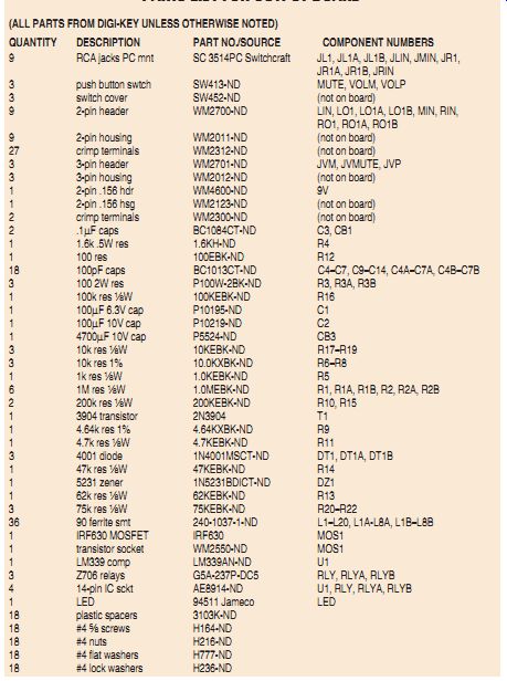
TABLE 2
PARTS LIST FOR OUTPUT BOARD
(ALL PARTS FROM DIGI-KEY UNLESS OTHERWISE NOTED)
QUANTITY DESCRIPTION PART NO./SOURCE COMPONENT NUMBERS 9 RCA jacks PC mnt SC 3514PC Switchcraft JL1, JL1A, JL1B, JLIN, JMIN, JR1, JR1A, JR1B, JRIN 3 push button swtch SW413-ND MUTE, VOLM, VOLP 3 switch cover SW452-ND (not on board) 9 2-pin header WM2700-ND LIN, LO1, LO1A, LO1B, MIN, RIN, RO1, RO1A, RO1B 9 2-pin housing WM2011-ND (not on board) 27 crimp terminals WM2312-ND (not on board) 3 3-pin header WM2701-ND JVM, JVMUTE, JVP 3 3-pin housing WM2012-ND (not on board) 1 2-pin .156 hdr WM4600-ND 9V 1 2-pin .156 hsg WM2123-ND (not on board) 2 crimp terminals WM2300-ND (not on board) 2.1µF caps BC1084CT-ND C3, CB1 1 1.6k .5W res 1.6KH-ND R4 1 100 res 100EBK-ND R12 18 100pF caps BC1013CT-ND C4-C7, C9-C14, C4A-C7A, C4B-C7B 3 100 2W res P100W-2BK-ND R3, R3A, R3B 1 100k res ¹/8W 100KEBK-ND R16 1 100µF 6.3V cap P10195-ND C1 1 100µF 10V cap P10219-ND C2 1 4700µF 10V cap P5524-ND CB3 3 10k res ¹/8W 10KEBK-ND R17-R19
3 10k res 1% 10.0KXBK-ND R6-R8 1 1k res ¹/8W 1.0KEBK-ND R5 6 1M res ¹/8W 1.0MEBK-ND R1, R1A, R1B, R2, R2A, R2B 2 200k res ¹/8W 200KEBK-ND R10, R15 1 3904 transistor 2N3904 T1 1 4.64k res 1% 4.64KXBK-ND R9 1 4.7k res ¹/8W 4.7KEBK-ND R11 3 4001 diode 1N4001MSCT-ND DT1, DT1A, DT1B 1 47k res ¹/8W 47KEBK-ND R14 1 5231 zener 1N5231BDICT-ND DZ1 1 62k res ¹/8W 62KEBK-ND R13 3 75k res ¹/8W 75KEBK-ND R20-R22 36 90 ferrite smt 240-1037-1-ND L1-L20, L1A-L8A, L1B-L8B 1 IRF630 MOSFET IRF630 MOS1 1 transistor socket WM2550-ND MOS1 1 LM339 comp LM339AN-ND U1 3 Z706 relays G5A-237P-DC5 RLY, RLYA, RLYB 4 14-pin IC sckt AE8914-ND U1, RLY, RLYA, RLYB 1 LED 94511 Jameco LED 18 plastic spacers 3103K-ND 18 #4 5/8 screws H164-ND 18 #4 nuts H216-ND 18 #4 flat washers H777-ND 18 #4 lock washers H236-ND
=======
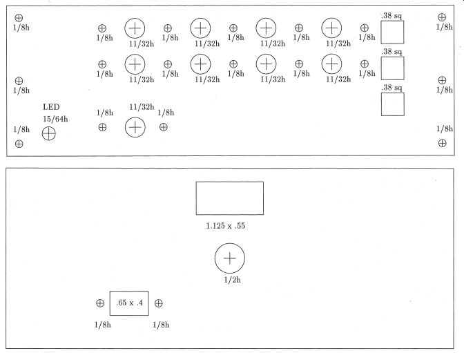
FIGURE 18: Templates used to machine the front and back panels of the
B2H10-001A enclosure, available from Lansing Instrument Corp. (90%)
----------------------
Also see:
Link | --A MODULAR HYBRID AMP SYSTEM