Component testing is a subject that was covered in "Getting The Most From Your Multimeter" (BP239) in some detail. In fact the whole of Section 2 in BP239 is devoted to the subject of component checking. Here we will consider this important topic in some detail again, carrying on from where BP239 left off. We will be concerned with the testing of components that were not covered in BP239, as well as more advanced methods of testing components that were covered by this earlier book. We will also look at a few quick but effective test methods that are not covered in BP239. These include a quick method of checking transistors.
Unijunction Transistors
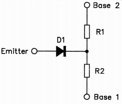
Figure 1.1
There seems to be few new circuits these days that utilize a unijunction transistor. These components offer a very simple means of producing an audio or infra-audio oscillator, timing circuit, etc., but have been largely ousted by the 555 timer integrated circuit and the low power versions of that device.
These offer better predictability and reliability, as well as being much more versatile. However, from time to time you may still find yourself building a project that uses one of these devices, particularly if you indulge in the increasingly popular pastime of building projects from old publications. Also, you may need to deal with one of these components if a project built some years ago should develop a fault. These devices once appeared in electronic projects for the home constructor almost as frequently as the 555 and its derivatives do today.
Internally, a unijunction transistor effectively consists of two resistors and a silicon diode connected in the arrangement shown in Figure 1.1. Note that connecting two resistors and a silicon diode in this configuration will not give you a circuit that will properly mimic a unijunction transistor. In its most common role as a relaxation oscillator, a unijunction transistor operates in a circuit of the type shown in Figure 1.2. Initially the single semiconductor junction (from which the device derives its name) is reverse biased, and C1 is able to charge up via RI. This continues until the charge voltage reaches about 0.6 volts more than the voltage at the junction of the internal potential divider of the unijunction. The semiconductor junction (i.e. the diode of Figure 1.1) then becomes forward biased.
This results in a regenerative action within the device that causes its base 1 to base 2 resistance to drop to a very low level.
This has several effects, one of which is to rapidly discharge C1 via the emitter - base 1 terminals of the unijunction and the low resistance of R3. This regenerative action does not occur if you use two resistors and a diode in a unijunction style circuit, and it is for this reason that a proper unijunction device is needed in order to get this type of oscillator to function properly. When the charge on C1 reaches a low level, the discharge current becomes too low to maintain the regenerative action, the unijunction switches off, and C1 starts to charge up again via R1 . This action continues indefinitely.
Pulse signals are generated across R2 and R3 due to one of the internal resistors of the unijunction effectively becoming a short circuit while the device is in the triggered state. This reduces the base 1 to base 2 resistance of the component, giving an increase in the voltage across the two base load resistors. There is also a non-linear sawtooth waveform (at what is often quite a high impedance) generated across C1.
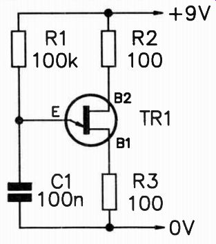
Figure 1.2
Probably the best method of checking a unijunction transistor is to connect it into a relaxation oscillator such as the one shown in Figure 1.2. It should not take more than a minute to breadboard a simple circuit of this type. You will need some means of detecting the audio output signal, but something as basic as a crystal earphone will suffice. If a relaxation oscillator of this type fails to oscillate it is often due to unsuitable component values rather than what could genuinely be considered a fault in the unijunction transistor.
With some circuits a wide range of frequencies have to be covered in a single range. This requires the use of a variable timing resistance which might have a minimum resistance of just a few kilohms running through to a maximum resistance that could be as high as a few megohms. If the timing resistance is made too low, the result is that the current through R1 is high enough to hold the unijunction in the "on" state.
This will clearly prevent oscillation from occurring. The result will be much the same if the timing resistance is too high, but with leakage currents preventing the device from triggering. If the device is held in the triggered state the measured voltage across C1 will be quite low, but if it is failing to trigger, the voltage across C1 will probably be 50% or more of the supply voltage (but you will need a high impedance voltmeter to stand any chance of getting an accurate reading). If you find that oscillation cuts off with a variable frequency oscillator of this type adjusted well towards one or other end of its frequency range, this almost certainly indicates a problem with the timing resistance becoming too high or too low for the particular unijunction in use. Under these circumstances the only way of obtaining satisfactory results might be to try a new unijunction transistor in the circuit.
This problem can also occur with fixed frequency oscillators where it has been necessary to use a very high or very low timing resistance for some reason. It might then be possible to obtain correct operation of the circuit by making the timing resistance lower and the timing capacitance higher, or the timing resistance higher and the timing capacitance lower, as appropriate. Provided any change in the value of one is matched by a proportional but opposite change in the other, the operating frequency of the circuit should remain unchanged.
If the timing resistor and capacitor are both very high in value, bear in mind that any lack of oscillation can be due to leakage in the capacitor. The same is also true of timer circuits that use a simple C - R timing network, and it is something that can afflict any timing circuit which uses a high value resistor and capacitor, not just unijunction circuits. What happens in these cases is that at some point the leakage current through the capacitor becomes equal to the charge current through the resistor. At this point the charge voltage ceases to rise, and the trigger point of the unijunction (or whatever) is never reached.
It is not practical to check for this problem by simply measuring the voltage across the timing capacitor to see if it has stopped rising. The current tapped off by the multimeter, even if it is a digital type with a resistance of about ten or eleven megohms, could well be high enough to ensure that the charge voltage would stop rising before the trigger potential is reached. Using the multimeter set to a high resistance range to make a leakage check on the timing capacitor is a more reliable method of checking for this problem. For satisfactory results to be obtained the leakage resistance of the capacitor would need to be about double the value of the timing resistor, and quite probably much higher in value than this. If a timing circuit or low frequency oscillator is unreliable or inconsistent in performance, this is usually indicative of problems with excessive leakage in the timing capacitor.
Capacitor leakage is a very common problem with simple timer circuits and very low frequency oscillators. Where possible use a non-electrolytic capacitor. The high values involved sometimes make this impractical, but tantalum bead capacitors often offer a solution to the problem. Failing that, an electrolytic component sold as a "low leakage" type should be used. Avoid very cheap or old components in critical applications such as this, as they often have very high leakage levels.
Transistor Resistance Checks
You can make a rough check on a unijunction device by making some resistance checks between its terminals. Data for unijunction transistors will specify the base 1 to base 2 resistance (the " RBB" parameter), and this can obviously be checked without any difficulty. This resistance is usually a few kilohms, and is between 4k7 and 9k1 for the popular 2N2646 unijunction for example.
From the emitter to either of the base terminals a diode action should be obtained, although the forward resistance …
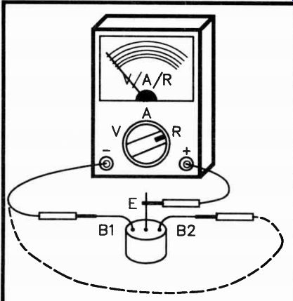
Fig. 1.3 Initial resistance check on a U.J.T.
… reading may be a little higher than usual due to the inclusion of about half the base 1 to base 2 resistance in series with the diode. In fact the deflection of the meter's pointer may be very small if you use a low resistance range. One having a centre scale reading of about 20k or more should be about right. Unijunction transistors are not usually symmetrical, and the emitter to base 1 resistance is likely to be a little higher than the emitter to base 2 resistance. Figures 1.3 and 1.4 show how to make these emitter - base checks, and the results that should be obtained.
If you are using a digital multimeter rather than an analogue type, remember that the test prods for each test must be …
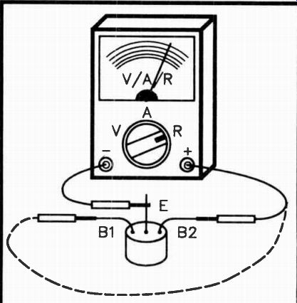
Fig. 1.4 The second pair of checks on a U.J.T.
… connected the other way round. Also remember that the test must be undertaken using the meter set to the "hi" setting, where appropriate, so that the test voltage is high enough to forward bias the semiconductor junction. This warning should also be heeded when making the resistance checks on semi conductor junctions that are described later in this Section.
This general method of checking unijunction transistors can be modified and used as a quick method of checking bipolar devices. The equivalent circuit of a bipolar transistor is a pair of back-to-back diodes connected as shown in Figure 1.5.
As can be seen from this diagram, the polarity of the diodes is different for n.p.n. and p.n.p. devices.
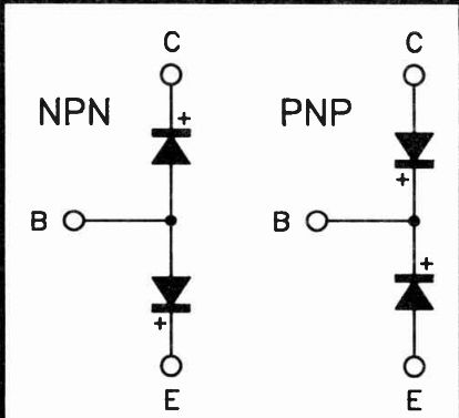
Figure 1.5.
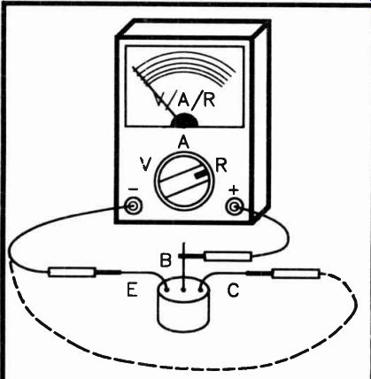
Fig. 1.6 Initial resistance checks on a bipolar transistor.
In order to test a transistor it is merely necessary to make some resistance checks across pairs of contacts in order to make sure that the correct diode actions are obtained. First the pair of checks detailed in Figure 1.6 should be made. This reverse biases the two diode junctions in turn, and should give an extremely high reading in both cases (probably an infinite reading). The next test (which is shown in Figure 1.7) forward biases both diode junctions, and should give the low resistance readings normally associated with a forward biased silicon junction. The final pair of tests are shown in Figure 1.8, and they check for a very high resistance between the collector and emitter terminals, regardless of which way round the test prods are connected. For both n.p.n. and p.n.p. devices the two diodes are connected with the opposite polarity, and whichever way round the test prods are connected, one or other of these diodes will block the current flow.
The checks in Figures 1.6 to 1.8 are for an n.p.n. test transistor, but the same method of testing can be applied to p.n.p. devices. However, the setup of Figure 1.6 will give low readings, while that of Figure 1.7 will give very high readings.
As pointed out previously, the tests of Figure 1.8 should produce high readings for either type of transistor.
Simple static tests of this type are obviously not 100% reliable. A device could pass these tests but still be deficient in some way. However, in practice a transistor which passes these tests is very likely to be fully serviceable, and not the cause of a fault. Things are more clear cut if a device fails one of these tests. If this should happen, there is very little chance of the component being fully functional. I will not say that it is impossible for a transistor to fail one of these checks and still be operational, but on the face of it this would seem to be totally impossible.
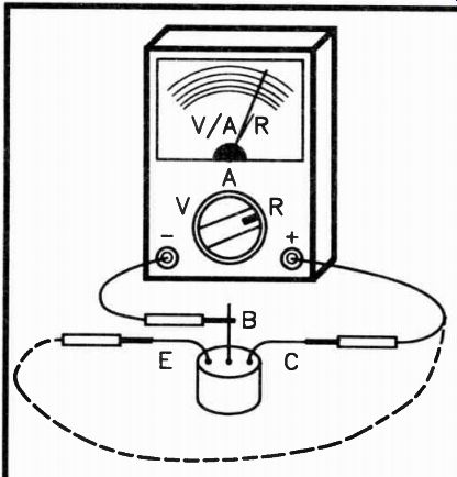
Fig. 1.7 The second set of resistance checks on a bipolar transistor
Fig. 1.8 Testing for a low leakage level
Another use of these tests is in finding out whether a transistor is an n.p.n. or p.n.p. device. It can also help to determine which lead is which on a device of unknown type number.
This can be useful when trying to sort out what's what in a bargain pack of "untested" transistors or "tested but unmarked" devices. First use trial and error to find a pair of terminals which do not provide continuity with the test prods connected either way round. These are the collector and emitter, but these simple resistance checks will not tell you which is which. Then try the tests of Figure 1.6. If high resistance readings are obtained, the test device is an n.p.n. type. Low resistance readings show that it is a p.n.p. type.
To determine which leadout is the emitter and which one is the collector, try subjecting the device to a current gain check with these terminals connected first one way round, and then the other. With one method of connection the transistor should provide a healthy level of current gain, while with the opposite method of connection it should have little or no current gain. Obviously the former is the correct method of connection. Provided the test voltage is only a few volts there is no real risk of damaging a silicon transistor by connecting it with the wrong polarity. This method would be a bit risky with germanium transistors though, and it is probably best not to try it with these.
S.C.R’s and I.C’s
This method of testing can also be applied to S.C.R’s - both thyristors and triacs. A thyristor is a four layer semiconductor which, as far as static resistance checks are concerned, is effectively two transistors connected as shown in Figure 1.9.
Both transistors are normally switched off, giving a very high resistance between the anode and cathode terminals, regard less of which way round the test prods are connected. The gate and cathode terminals are effectively the base and emitter terminals of an n.p.n. transistor, and as such provide a diode action. In fact when subjected to resistance checks, a thyristor behaves in almost exactly the same way as an n.p.n. transistor, with the gate, anode, and cathode respectively acting as the base, collector, and emitter. There is one difference though, and this is that there is a high resistance from the gate to the anode whichever way round the test prods are connected. An n.p.n. transistor provides a diode action between its base and collector terminals.
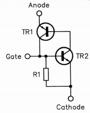
Fig. 1.9 The equivalent circuit for a thyristor.
Once again, this method of testing can be used to help identify the terminals of a device which has an unknown leadout configuration. Use trial and error to find two terminals that provide a diode action. These are the gate and cathode terminals, and from the polarity of the junction you can deduce which is which. The other terminal is obviously the anode.
Results are similar if a triac is tested using the same resistance checks, but with the MT2 terminal taking the place of the anode, and the MT1 terminal taking the place of the cathode. However, as a triac is a bidirectional device, its gate to MT1 terminals will act as a forward biased diode whichever way round the test prods are connected. This complicates matters if you use these tests in an attempt to identify the leadouts of a device which has an unknown leadout configuration. There is no way of ascertaining which is the gate and which is the MT1 terminal since there is continuity between these terminals with the test prods connected either way round.
Integrated Circuits
Integrated circuits are notoriously difficult to test. As we shall see shortly, it is possible to test some of the more simple analogue and digital devices by rigging up a basic test circuit and making a few voltage checks. This approach is inapplicable to many integrated circuits though, as their functions are far too complex to be tested in such a fundamental manner. It is possible to apply resistance checks to integrated circuits though, and in many cases this will produce useful results. The only problem in using this type of testing is that the complexity of many integrated circuits makes it difficult to determine what sort of resistance readings should be present between any two given terminals. Being realistic about it, the only way of overcoming this problem is to make checks on a device that is known to be fully functioning, so that you have something against which tests made on a suspect device (or devices) can be made.
There is a potential flaw in this system in that much of the circuitry in an integrated circuit is well removed from any of the pins. A major fault in a part of the circuit that only connects to one of the pins via a very indirect route may not show up in resistance checks. In practice a lot of faults in integrated circuits occur due to excessive input and output currents, or similar problems, and the damaged circuitry will be in parts of the device which connect directly to one or more of its pins. Also, where a breakdown does occur some where in the middle of a complex integrated circuit, the result is often a chain fault which results in much of the circuit being destroyed. This is likely to show up quite clearly on resistance checks. You still need to bear in mind that resistance checks on semiconductor devices are not totally conclusive. If a device passes the checks it could still be below specification.
If a device fails a test, then it is almost certainly a "dud". Testing the resistance from every pin to every other pin of an integrated circuit, with the test prods connected both ways round, is probably not a practical proposition. Even with an eight or fourteen pin device it could take quite a long time, and with a forty pin integrated circuit it would take an inordinate amount of time. Probably the best approach is to measure the resistance between the 0 volt supply pin and every other pin, and then repeat the procedure with the test prods reversed. Obviously you will not be able to memories the results of numerous resistance checks, and will have to write down the test results obtained from the standard device against which others will be judged. A simple chart, as in the example shown here, is probably the best way of writing down your results.
--------------
Pin Number Negative Prod Positive Prod
To 0 Volt To 0 Volt
1 5.5k 500k 2 5.5k 500k 3 4.5k 500k 4 5.5k 500k 5 4.5k 500k 6 5.5k 500k 7 4.5k 500k 8 5.5k 500k 9 4.5k 500k
10 0 Volt Pin 0 Volt Pin
11 5.5k 500k 12 4.5k 500k 13 5.5k 500k 14 4.5k 500k 15 5.5k 500k 16 4.5k 500k 17 5.5k 500k 18 4.5k 500k 19 5.5k 500k 20 3.5k 180k
------------------
Dangers
There are a few points to keep in mind when trying this type of testing. One is that it works better with bipolar integrated circuits than it does with CMOS, NMOS, or PMOS types. It will actually work quite well with these MOS integrated circuits, but only if they have pull-up resistors on the inputs.
What can happen otherwise is that stray and varying voltages on the inputs result in the resistance readings you obtain varying over wide limits. This obviously makes a set of test results of dubious worth, and difficult to take anyway.
Another point about MOS devices which do not have pull up resistors at inputs, or some other effective form of static protection, is that they are vulnerable to damage due to static charges. Making measurements on a device which is out of circuit and not in its protective packaging is a bit risky, especially if it is a highly complex and costly component.
There are ways of reducing the risk, one of which is to fit the test component onto a breadboard which is wired so that each pin of the device is connected to a common "earth" rail via a high value resistor (around 5.6 to 10 meg-ohms should suffice). This should prevent any large voltage build-ups on the pins so that the device is kept safe. It should also prevent any stray voltages reaching sufficient amplitude to operate any of the inputs, and in this way the varying readings mentioned previously are avoided. It is a good idea to fit the test device onto a breadboard anyway. You can then use a short piece of wire and a crocodile clip lead to make the connection to the 0 volt pin of the device, leaving both hands free to connect the other test prod to the remaining pins and to note down results.
Another method of protecting static sensitive devices is to push their pins into a piece of conductive foam (the black foam material in which many integrated circuits are supplied these days). In my experience this material does not conduct particularly well, and it will not have a significant affect on the resistance readings. This method has the disadvantage that it is a little slower and more difficult to make the connections to the pins and note down the results.
When checking delicate integrated circuits you must be careful about the choice of measuring range. A low range is undesirable as it could produce quite large current flows that could damage the test components. A high resistance range is not a good choice as the test voltage could be high enough to damage the test components (but this depends on the type and model of multimeter in use). A range having a mid-scale value of about 20k should be suitable. When testing very delicate devices it is probably best to only take measurements with the positive test prod (or negative prod of a digital instrument) connected to the 0 volt supply pin. This avoids applying a voltage of the wrong polarity to the other pins of the device.
Wherever possible, the best method of testing any complex integrated circuit is to plug it into a circuit that is known to be fully functioning, and then see if the device functions properly in this circuit. However, in practice this might not be too easy to achieve. Very often you will not know for certain whether the main circuit is alright and the integrated circuit is at fault, or vice versa, or perhaps they are both faulty. Plugging a new integrated circuit into part of a circuit that does not seem to be functioning properly may seem to be the obvious course of action, but do not be in too much of a hurry to plug an expensive integrated circuit into a circuit board that caused the demise of the original integrated circuit, as fitting a replacement device could just lead to this new component being instantly "zapped" at switch-on! If you think you have located a faulty integrated circuit, it is always a good idea to make a few checks to determine whether or not there is a fault on the board which caused the damage to the device.
Integrated circuits are very reliable, and failures are often due to something like an excessive supply voltage due to a power supply fault.
LC Test Circuits
Rigging up a breadboarded test circuit for a complex integrated circuit will usually be an impractical proposition, but many of the more simple types can be tested in this manner.
When a fault is proving to be difficult to locate, testing the semiconductors, preferably with them completely removed from the circuit board, is always a good idea. If one or more of the semiconductors proves to be faulty, then replacing the faulty component or components will probably cure the problem (but note the warning given previously). If the semi conductors prove to be fully serviceable, then you know that the problem is in the passive components or the soldering, and you can go on to check these.
As I have pointed out many times before, and will no doubt explain many more times in the future, if a newly constructed project fails to work, probably more than nine times out of ten it is due to a bad joint, a short circuit due to a solder splash, or something of this nature. With a newly constructed project where the semiconductors prove to be functioning correctly, the board itself is probably the part of the unit to concentrate on next. With a project that has worked correctly but has become faulty, the passive components would represent the most likely cause of the problem.
For the checks described here the particular breadboard used is not too important. The test circuits are so simple that virtually any breadboard should suffice, but it obviously needs to be a reasonably modern type capable of taking integrated circuits with 0.1 inch pin spacing (or one fitted with a carrier for standard dn. integrated circuits). Operational amplifiers represent one of the most simple types of integrated circuit as far as testing is concerned. They are easily tested by using them as voltage comparators, as in the simple test circuit of Figure 1.10. An operational amplifier is a differential amplifier, which simply means that it amplifies the voltage difference across its inputs. If the non-inverting (+) input is at a higher voltage than the inverting (-) input, the output goes positive. If the relative input voltages are reversed, the output goes positive. In practice the d.c. voltage gain of an operational amplifier that is used open loop (i.e. without any negative feedback) is very high, being typically about 200,000 times. Therefore, only a minute voltage difference is needed across the inputs in order to send the output fully positive or negative.
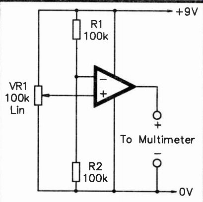
Figure 1.10
In the test circuit of Figure 1.10 a fixed potential of about half the supply voltage is fed to the inverting input of the test device by the potential divider circuit formed by R1 and R2.
VR1 permits a variable voltage to be fed to the non-inverting input. If VR1 is initially set for minimum voltage at its wiper, and then steadily advanced, the output voltage from the circuit should initially be quite low, but should suddenly jump to almost the full supply voltage with VR1 at roughly the middle of its adjustment range. Due to the very high open loop gain of an operational amplifier, it should be virtually impossible to set VR1 to give an intermediate output voltage.
In fact with many operational amplifiers it may well prove to be totally impossible to obtain an intermediate output voltage.
Do not expect the maximum and minimum output voltages from the operational amplifier to be equal to the positive and negative supply potentials. With most operational amplifiers (including the standard pA741C and most of its bipolar and f.e.t. equivalents) the maximum output voltage falls about 1 volt or so short of the positive supply potential. The minimum output voltage is often more than 2 volts, but with some MOS and bipolar types (such as the CA3130E, CA3140E, LM358, and LM32) the minimum output voltage can go to within a few millivolts of the negative supply voltage. Modern operational amplifiers almost invariably have good immunity to latch-up. This is where the output voltage goes to the wrong level because the differential input voltage is excessive, or one or both inputs are taken outside their normal operating voltage range. This latch-up could result in the output going high with VR1 set for around minimum voltage, or low when it is set for about maximum voltage (i.e. jumping to the wrong state at the extremes of VR1's adjustment range). Few non obsolete devices suffer from this problem though, and it would be as well to be suspicious of any modern device that does have this trait.
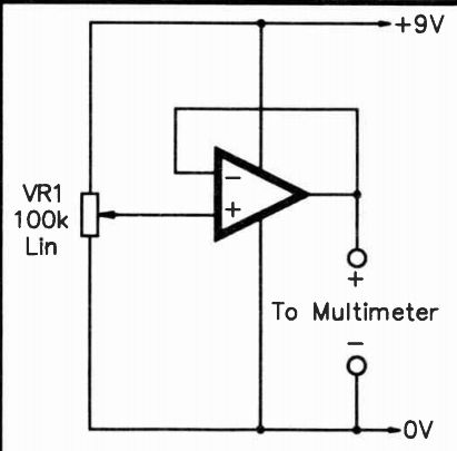
Fig. 1-11 Testing an op. amp. connected as a voltage follower
Another very simple but useful test for operational amplifiers is to try them as voltage followers, as in the test circuit of Figure 1.11. With 100% negative feedback from the output to the inverting input of the amplifier, it has unity voltage gain from the non-inverting input to the output. VR1 can be used to set any input voltage between 0 volts and 9 volts, and in theory the output voltage measured on the multimeter should be exactly the same as the input voltage. In practice the output voltage limitations of the operational amplifier must be taken into account. As pointed out previously, for most devices this means that the minimum output potential will be about 2 volts, and the maximum will be around 1 to 1.5 volts less than the positive supply voltage. With appropriate types, the minimum output voltage will be insignificantly more than 0 volts.
Adjustment of VR1 should give a smooth variation between the output voltage limits imposed by the test device. If the output voltage tends to jump all over the place, or simply stays fully positive or negative, this indicates that the test device is faulty.
Apart from operational amplifiers, there are probably not many linear integrated circuits which lend themselves well to simple test setups of this type. It is a technique that can be used with some audio power amplifiers though. Some modern audio power amplifier integrated circuits are effectively high power operational amplifiers, and the test circuits of Figures 1.10 and 1.11 should work perfectly well with these. With a device such as the LM380N, which has built-in bias components, this method of testing is not applicable.
However, it would be quite feasible to fit the device onto a breadboard and connect it to a 9 volt supply. If its biasing is working correctly, the output voltage should be within a few percent of half the supply voltage.
Digital I.C’s
Simple static testing circuits are easily applied to many types of digital integrated circuit, including gates, decoders, multiplexer, etc. On the other hand, there are some logic devices that are essentially dynamic in their function, and which can not be fully tested by taking d.c. voltage checks. The techniques described here can be used to good effect with most of the digital integrated circuits used in home constructor designs though.
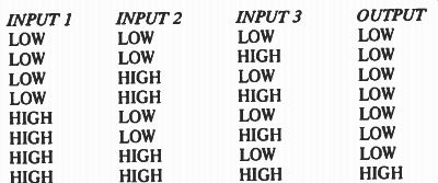
The basic action of many digital integrated circuits is to produce a certain output state, or set of output states, for a given set of input logic levels. Gates, inverters and decoders, for example, fall into this category. The usual way of showing the function of these more simple logic devices is by way of a "truth table". In its most basic form this just consists of a list of input states, with the output state or states being shown for each set of input conditions. For instance, this is the truth table for a three input AND gate.
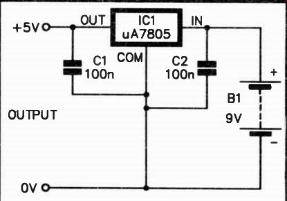
Figure 1.12.
Integrated circuits of this type are easily tested with the aid of a breadboard, a power source, a multimeter, and a few link wires. First wire the supply pins of the chip to a suitable power source. For most logic devices this means a 5 volt supply, and virtually all modern bench power supplies can provide a 5 volt output. Improvising a temporary power source using batteries is not easy as 1.5 volt cells can obviously not provide 5 volts. Three cells gives about 4.5 volts, or four cells gives around 6 volts. When testing logic integrated circuits you need to bear in mind that many of them are only guaranteed to operate with a supply voltage that is within a few percent of the specified supply potential. The acceptable voltage range depends on the logic family from which the test device is taken. Note that the supply voltage range is not the same for all the logic families under the general TTL heading ("LS", "HC", "HCT", etc.). Some of the CMOS TTL devices have relatively wide supply voltage ranges, and should operate properly with a 3 volt, 4.5 volt, or 6 volt battery supply.
With many logic families there is only a 5% tolerance on the supply voltage (i.e. it should be between 4.75 and 5.25 volts). In practice a 4.5 volt or 6 volt supply is likely to be satisfactory for static tests, but it is obviously better if the supply voltage is within the chip manufacturer's recommended operating range. The results of tests are then conclusive. A simple way of providing an accurate 5 volt supply is to use a 9 volt battery plus a 5 volt monolithic voltage regulator, as in the circuit of Figure 1.12. The additional components should be easily accommodated on the breadboard.
Testing ordinary CMOS logic circuits is less problematic.
The operating voltage range of old devices is about 3 to 15 volts, and with modern types the acceptable supply voltage range is 3 to 18 volts. A 3, 4.5, 6, or 9 volt battery supply is adequate for testing purposes. Some TTL devices have quite high supply currents even under static operating conditions, but the quiescent current consumption of most CMOS devices, including many of the more complex ones, is negligible. A small (PP3 size) 9 volt battery is therefore perfectly suitable as the power source.
Having connected the supply, the next step is to use the link wires to set pp the first set of input states. Simply connect inputs to the positive supply rail if they must be taken high, or to the negative supply if they must be set to the low state. The multimeter is then used to measure the output voltage or voltages, to ensure that they are correct. Then the link wires are adjusted to set up the next set of input states, the output voltage should be checked again using the multi meter, and so on until the output voltage has been checked for every set of input states.
This can be rather time-consuming, especially when you consider that each integrated circuit may contain several gates.
In fact it is the single gate chips with numerous inputs that require the longest test procedures. An eight input gate for instance, has some two hundred and fifty-six different input states. With devices of this type it is probably best to rationalize the test procedure to a considerable degree in order to make the task more manageable. Suppose that an eight input NAND gate must be tested. The basic action of this device is to provide a low output level unless all eight of its inputs are high. Obviously only testing all two hundred and fifty-six input conditions would give definite proof that the device was fully functioning, but a good rationalized test procedure would be to first check that the output was low with all eight inputs tied to the high state. Next input 1 would be taken low, and a check made to see if the output had gone low. Then input 1 would be returned to the high state, and input 2 would be taken low. The output level would then be checked again.
Next input 2 would be returned to the high state, input 3 would be taken low, the output voltage would be checked, and this procedure would be continued until all the inputs had been tested in the low state. If each input was able to exercise control over the output, then it would be highly unlikely that the device was faulty. This is the rationalized truth table for an eight input NAND gate.
------------
Logic Voltages
In order to interpret the results of this form of testing you need to know the valid voltage ranges for the logic 0 and logic 1 levels. When testing the CMOS 4000 range of integrated circuits there is no great difficulty here. Logic 0 ("low") should give a voltage reading that is so low it will probably fail to register on the meter, while logic 1 ("high") should give a reading that is virtually equal to the positive supply potential. This is due to the use of complimentary output transistors, which gives the effective output circuit of Figure 1.13(a) when an output is high, and that of Figure 1.13(b) when it is low. The low value resistor is the resistance of the transistor that is switched on, while the very high value resistor is the resistance of the transistor that is switched off.
The very high "on" to "off" resistance ratio of the output transistors ensures that the unloaded peak-to-peak output voltage is not significantly less than the supply voltage.
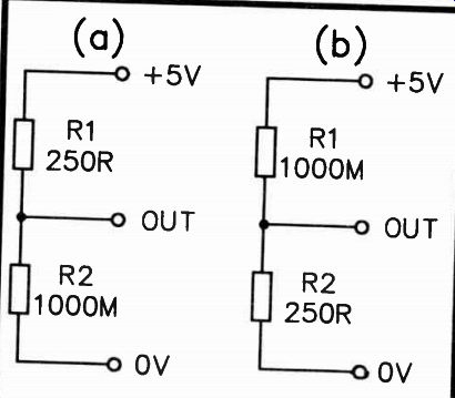
Fig. 1.13 CMOS equivalent output circuits
In CMOS data books you will not find that the high and low logic levels are stated as being within a few millivolts of their respective supply voltages. Logic 0 is usually given as something like 0 to 30% of the supply potential, with logic 1 at anywhere between 70 and 100% of the supply voltage.
These are voltage ranges to which the inputs of a CMOS device are guaranteed to respond properly. With the outputs of CMOS devices switching almost fully between the two supply levels, this may all seem to be of academic importance.
However, you must remember that in normal use CMOS outputs may be switching between the two logic levels at a high frequency, and they may then fail to reach the same voltage levels that are achieved in static tests. Perhaps of more relevance in the current context, CMOS outputs are sometimes loaded more heavily than the very light loading provided by a multimeter or several CMOS inputs. The input resistance to CMOS logic devices incidentally, is about a million megohms.
This gives what for practical purposes can be regarded as infinite fanout under d.c. conditions, but due to input capacity the dynamic fanout is about fifty.
If a CMOS logic integrated circuit produces the right unloaded output voltages, the chances are that it is fully functioning. Results are not totally conclusive though. I have encountered CMOS devices in the 4000 logic family that do not work when plugged into a circuit that operates at medium to high speeds, but which seems to be perfectly alright when subjected to static and low frequency tests. I have heard of others encountering the same problem, and so this is presumably a reasonably common type of fault. The cause of the problem seems to be that an overload on the output has caused an excessive output current which has damaged one of the complementary output transistors. This then provides a high resistance load for the other transistor which acts as a simple common source switch having a resistive load. Under static tests this might give quite plausible results, but at frequencies of more than a few hertz the output stage fails to work due to the low "on" output current and stray capacitance slowing down the switching time to inadequate level.
A safer method of making static tests on CMOS logic integrated circuits is to connect the multimeter to a potential divider connected across the supply rails, and to then connect this to each of the test points in turn via a link-wire, as in Figure 1.14. The potential divider tries to pull the test point to about half the supply voltage, but the output under test tries to pull the test point high or low. The output, if it is functioning correctly, will largely win the battle, as its output transistors can provide a resistance that is significantly lower than the value used in the potential divider. The output voltages will fall significantly short of either supply voltage, but will be well within the acceptable ranges of 0 to 30% and 70 to 100% of the supply voltage. If one of the output transistors is damaged, then one of the logic levels will be achieved properly, but with the output set to the other logic state the output voltage will be about half the supply voltage.
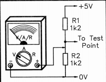
Figure 1.14
TTL Outputs
The acceptable output voltage range for TTL devices varies slightly from one type to another. However, in general, and for types which operate from a 5 volt supply, a logic 0 level is anything from 0 to 0.8 volts, and a high level is anything from 2 to 5 volts. This gives a relatively narrow range of illegal voltages, but in practice an unloaded TTL output will be little more than 0 volts when it is low, and around 4 volts when it is high. Faults in the output stages of TTL devices, in my experience anyway, seem to be more rare than those in CMOS types. It would probably still be a good idea to use the method of loading described previously when testing TTL integrated circuits though.
If you are testing TTL devices that can operate on a supply potential of other than 5 volts, and you are having to use a supply voltage of other than 5 volts, then the acceptable voltage levels for each logic level must be adjusted proportionately in order to match the change in supply voltage. You could consult the data sheet/book for the device concerned if you want more accurate information about the valid voltage ranges for various supply voltages. However, in practice the outputs will probably go to what are clearly acceptable voltages or completely invalid potentials, making any highly accurate voltage tests unnecessary.
Instate Outputs
There is a slight complication when testing many logic integrated circuits in that they have "tristate" outputs, or "three state" outputs as they are also known. Apart from the usual high and low levels, these have an "off" state. In this state the output has a very high output impedance, and it goes to a logic level determined by some other device. This other device is usually the output of another logic element, an input, or a pull-up/pull-down resistor.
Testing a tristate device should not present any real difficulties, and it is again just a matter of including the potential divider in the test circuit. High and low logic levels will produce the appropriate voltage levels, while the "off" state should result in the output being taken to around half the supply voltage by the potential divider circuit.
Decoders Etc.
Obviously many logic integrated circuits are not simple gates and inverters, and provide more complex tasks. Despite this, many logic devices can be tested using simple static voltage checks. As an example, take the popular 74LS138 three to eight line decoder integrated circuit. This has the pinout arrangement illustrated in Figure 1.15.
The basic function of this device is to activate one of the outputs ("0" to "7"), with the activated output being selected by the binary number fed to the three main inputs ("A" to "C"). Input "A" is the least significant bit - input "C" is the most significant bit. "000" on these inputs would activate output "0", 001 activates output " 1", 010 activates output "2", and so on through to 111 activating output "7". The outputs are all active low types, so the activated output is low while all the others are in the high state.
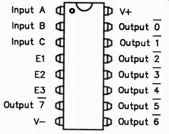
Fig. 1.15 The 74LS138 pinouts. This device can be tested in much the same
way as logic gates.
Testing a device of this type does not pose any real problems, and the same basic techniques that are used with gates would seem to be equally applicable to a device of this type.
It is just a matter of wiring the inputs, in turn, to each of the eight different sets of input states. For each set of input conditions the outputs must be checked to ensure that the right one, and only the right one, is in the low state.
There is an added complication in that the 74LS138 has three enable inputs; two negative ones (pins 4 and 5) and one positive type (pin 6). When carrying out the test procedure described above it would be necessary for each of these to be taken to their active state. If the initial test procedure gave positive results, it would then be necessary to test the enable inputs. This is just a matter of measuring the output voltage from the activated output, using the potential divider loading described previously. In turn, the three enable inputs are then taken to their non-active states, which in each case should result in the output voltage going to about half the supply voltage (i.e. the output should go to the "off" state).
Static Dynamic Testing
Using a multimeter it is obviously not possible to undertake high speed dynamic tests on logic integrated circuits. On the other hand, it is quite possible to slow down the operating speed of a test circuit to the point where a multimeter can be used to check that outputs are at the correct logic levels. This is a sort of cross between true dynamic and true static testing.
The multimeter is measuring static voltages, but they need only be maintained for a second or two, after which the circuit is clocked on to the next phase by an input pulse so that the next voltage check can be made.
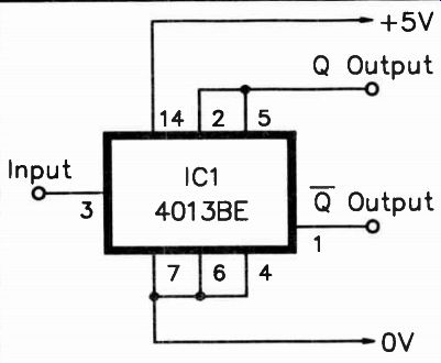
Fig. 1.16 Connecting a D type flip-flop as a divide by two circuit enables
it to be tested.
As a simple example of how this type of testing can be undertaken, consider the circuit of Figure 1.16. This has one half of the 4013BE dual D type flip/flop connected as a divide by two circuit. In common with most flip/flops (and several other types of logic circuit elements) this one has two outputs.
These are the "Q" and "not Q" outputs (the latter having the "not" bar over the Q). They differ in that the Q input is active high, whereas the not Q output is active low. On successive input pulses the Q input should be toggled from one logic level to the other, and the not Q input should always be at the opposite state.
Testing this circuit requires a low frequency input signal at about one pulse every two to five seconds. Most logic pulsers can provide a signal of this type or a simple clock oscillator can be breadboarded together with the rest of the circuit. A suitable circuit based on the ever useful 555 timer integrated circuit is provided in Figure 1.17. Another alternative, and quite a good one, is to use a push button switch to permit input pulses to be generated manually. The only problem with this method is that contact bounce tends to result in push button switches generating numerous spurious output pulses. These would obviously result in misleading results, and they must be suppressed. This is easily done using a simple active debouncing circuit, as in the circuit of Figure 1.18.
Monitoring the two outputs of a flip/flop presents a slight problem. One solution is to use a low enough clock frequency to permit the multimeter to be used to measure both voltages, in turn, between clock pulses. If you have two multimeters, and a lot of people these days have both analogue and digital instruments, then there is obviously no difficulty. Use one multimeter to check the Q output, and the other to test the not Q output. Another method is to measure the voltage across the two outputs. Assuming that a 5 volt supply is used, the differential output voltage should alternate between +5 volts and -5 volts. Obviously this method is only possible if you are using a digital multimeter, or one of the few analogue types that can handle input voltages of either polarity.
To test the divide by two flip/flop circuit, check that each input pulse results in both outputs changing state. Pin 4 is the …
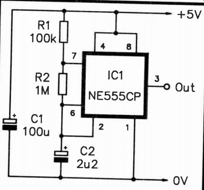
Fig. 1.17 A low frequency clock oscillator based on the 555 timer.
… reset input, and if this : s taken high it should result in the Q output going low and the not Q output going high. The divide by two action will be inhibited while the reset input is high. If the reset input is returned to the low state, and the set input (pin 6) is taken high, the Q output should be forced high, the not Q output should be forced low, and the divide by two action should again be inhibited.
These methods of testing can be applied to other logic integrated circuits, including some that, on the face of it, represent what might reasonably be termed a testing time.
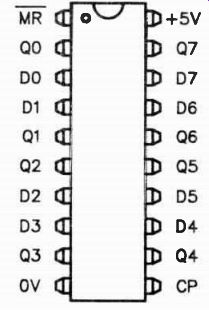
A 74LS273 8-bit D type flip/flop is a good example of an integrated circuit which falls into this category. This is quite a complex device which has the pinout configuration shown in Figure 1.19.
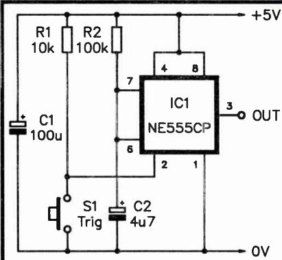
Fig.1.18 A simple debouncer circuit based on a 555 timer
Probably the most common application of this device is as an eight bit data latch. When used in this role the eight data inputs ("DO" to "D7") are fed from something like the data bus of a microprocessor. A negative pulse from the address decoder or other control logic circuit is applied to the "CP" (clock pulse) input in order to latch the bit pattern on the eight inputs onto the eight outputs ("QO" to "Q7"). The MR input is the master reset input, and taking this low sets all the outputs low and inhibits the device.
The obvious first test on this device is to take the master reset terminal low, and to check that this sets all the outputs low. Then set up a bit pattern on the inputs by (say) wiring DO to D3 low, and D4 to D7 high. Applying a pulse to the clock pulse input should result in this bit pattern being transferred to the outputs. lf the device is providing the correct latching action, changing the bit pattern at the inputs should have no effect on the bit pattern on the outputs.
With a little ingenuity it should be possible to test virtually any logic integrated circuit, including such things as multi-bit latches, magnitude comparators, and multiplexer. You need to be familiar with the functions of the devices you are trying to test though, and as with most testing, the better your technical knowledge the greater your chances of carrying out the task successfully.
Component Analysis
In BP239 a method of using a multimeter plus a few other components as a transistor current gain meter was described.
This basic concept can be extended to permit virtually any static parameter of a transistor to be checked, and it can also be used with other components. Suppose that you wish to test the gain of a transistor at specific collector voltage and current levels, because your data on the device only gives a gain range at these figures. Also, you may wish to make a test of this type if you need to test some high power transistors that can not be tested conclusively using many transistor checkers. The test setup of Figure 1.20 should give the desired result.
The variable voltage power supply is adjusted to give the required collector voltage, and VR1 is adjusted for the required collector current, as registered on multimeter 2. This current reading is then divided by the base current reading obtained on multimeter 1 in order to obtain the current gain of the test transistor. As an example, suppose the collector current is set at 100 milliamps and that the measured base current is 850 microamps (0.85 milli-amps). Dividing 100 milliamps by 0.85 milliamps gives the d.c. current gain figure of about 118 (100/0.85 = 117.64). Obviously this test setup calls for two multimeters, but if you only have one multimeter it is still usable. Start with a shorting link in place of multimeter 1, and then adjust VR1 for the correct collector current. Then use the meter in position one, and use a shorting link for multimeter 2. This enables the base current to be measured so that the current gain calculation can be made. If you wish to be pedantic, you can use resistors instead of shorting links in order to mimic the resistance of the multimeter. You can also adjust the supply voltage slightly higher in order to compensate for the voltage drop through multimeter 2, and thus give exactly the required collector voltage. In practice this sort of thing is probably not worthwhile, and is unlikely to give much improvement in the accuracy of results.
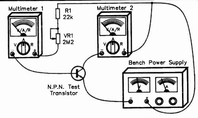
Fig. 1.20 A comprehensive transistor gain testing setup.
This sort of improvised setup can be used to test the more obscure aspects of semiconductors. Suppose you have a thyristor which is not behaving as expected, but passes the resistance checks described previously, and seems alright when subjected to a simple trigger test (as described on page 60 of BP239). One possibility would be that the hold-on characteristic of the device is not within the specified limits.
Remember that a thyristor, unlike a transistor, remains switched on even if the input current is removed. It can only be switched off by reducing the current flow between the anode and cathode terminals below a certain threshold level.
This is called the "hold-on" or "holding" current, or is usually termed "Ihm" in thyristor data sheets and books.
The holding current could be checked using the simple test circuit of Figure 1.21. VR1 is initially set at minimum resistance so that a fairly high current flow is produced when the test device is triggered. To trigger the thyristor it is merely necessary to momentarily operate push button switch PB1.
In fact you do not need to have a push button switch here - briefly fitting a shorting wire in this part of the circuit will trigger the thyristor. Once it has been triggered, the multi meter should register the anode current, and this current should be maintained when the trigger current to the gate is removed. By adjusting VR1 it is possible to vary the anode current, and it is a matter of slowly adjusting this control for a reducing anode current while carefully monitoring results on the multimeter. At some stage the current reading will suddenly drop to zero. The holding current is the reading that was obtained just before the meter indicated zero current flow.
If the holding current is very low, the cut off might not be obtained even with VR1 adjusted for maximum resistance.
Adding another fixed value resistor in series with VR1 will permit lower currents to be accommodated by the test circuit.
Alternatively, you might simply decide to temporarily short circuit the anode and cathode terminals of the thyristor to reduce the anode current to zero, to check that the device does not have a tendency to stick in the "on" state.
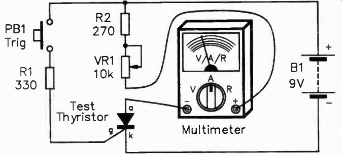
Fig. 1.21 A setup for testing thyristor holding current
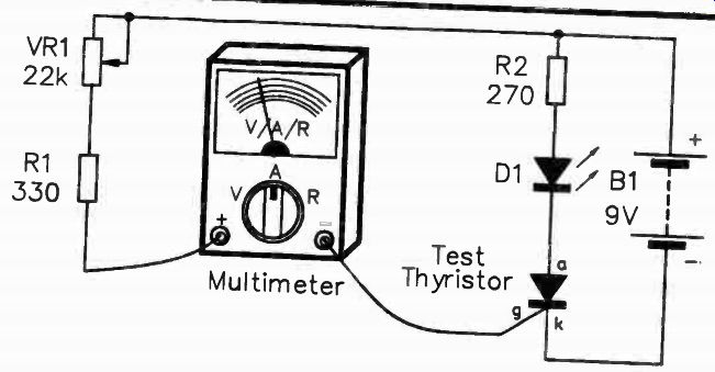
Fig. 1.22
Another important thyristor parameter is the maximum gate trigger current ("Ig" in the data books). Note that this figure is not the maximum permissible gate current, but the maximum input current that will be needed in order to trigger the device. With many modern thyristors this figure is only a fraction of a milliamp, whereas it is typically about 20 to 30 milliamps with most of the older types. Using a type that has a high trigger current could obviously prevent the circuit from operating if it is designed for a modern high sensitivity type.
The gate trigger current can be measured using the test circuit of Figure 1.22. This time start with VR1 at maximum resistance, and slowly advance it until l.e.d. indicator D1 lights up (which indicates that the ,thyristor has triggered). The reading on the multimeter then indicates the gate trigger current at which the device is activated.
There are plenty of pieces of test gear for testing components such as diodes, transistors, resistors, and capacitors, but you can not expect to have specialist test equipment to cover all component testing. The range and diversity of modern electronic components is such that even if a full range of component testing equipment could be purchased or home constructed, so many pieces of equipment would be needed that it would not be a practical proposition to do so. In practice you are unlikely to find test equipment to meet all your component testing requirements anyway. Simple breadboard test circuits utilizing one or two multimeters represent a versatile and inexpensive solution to the problem.
If you understand the function of a component and its d.c. characteristics, then it will almost certainly be possible to test it using a simple improvised test circuit.
L.E.D’s and L.C.D’s
The testing of light emitting diodes was covered in BP239. It is basically just a matter of switching the multimeter to a suitable resistance range and connecting it to the 1.e.d. with the appropriate polarity. If the l.e.d. is functioning correctly it should light up. This method of testing should work equally well with seven segment displays and bargraph types. The segments of a seven segment display are given identifying letters from "A" to "G", and the decimal point is usually just abbreviated to " DP". Figure 1.23 shows the standard arrangement of the segments in one of these displays.
When testing a common cathode type, connect the positive test prod to the cathode terminal, and then touch the negative test prod onto each of the other terminals in turn to see if the appropriate segments light up. For a common anode display, connect the negative test prod to the anode, and the positive test prod to each of the cathodes. This assumes you are using an analogue multimeter - the test prods must be connected the other way round if you use a digital type.
Infra-red 1.e.d.s, as used in remote control systems etc., pose a slight problem. All the components of this type I have encountered fail to produce any visible light output at all.
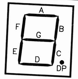
Fig. 1.23 The segment layout for a seven segment display.
These are easily checked using the resistance range of a multimeter.
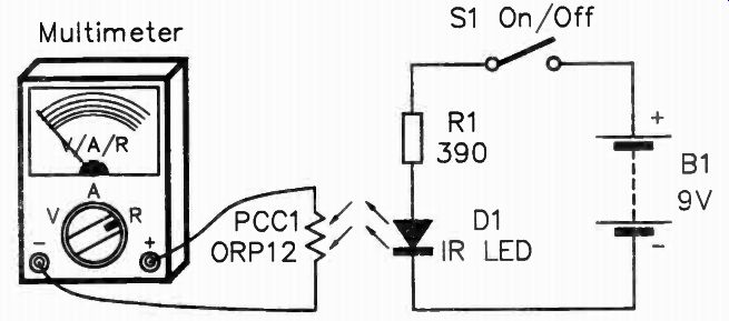
Fig. 1.24 Even something as awkward as an I.R.L.E.D. can be tested with a
little ingenuity.
However, simply testing that an infra-red 1.e.d. provides a diode action should give a good indication of whether or not the component is functioning properly. If it does not provide a diode action, then it is certainly faulty. If it does, then it is possible but highly unlikely that it is faulty.
As a more comprehensive test you could try the simple test circuit of Figure 1.24. This uses a 9 volt battery and current limiting resistor R1 to bias the infra-red diode into conduction.
Its infra-red output is directed at photocell PCC1, which is the ever popular ORP12 cadmium sulphide cell, but virtually any other cadmium sulphide photo-resistor should be suitable. The resistance of PCC1 is measured using the multimeter. If the battery is disconnected from the infra-red 1.e.d. its output will be cut off, the light level reaching PCC1 will decrease, and a higher reading should be shown on the multimeter. It is not necessary for this test to be carried out in near or total dark ness, but you should try to keep the photocell shielded from my strong sources of light. The lower the ambient light level reaching PCC1, the more pronounced the change in PCC1's resistance should become.
Although cadmium sulphide photo-resistors are often thought of as only visible light detectors, they offer good sensitivity at the light wavelengths produced by infra-red light emitting diodes. In common with many photo devices, most cadmium sulphide photocells offer peak sensitivity to this part of the spectrum.
Liquid crystal displays (l.c.d’s) represent a difficult type of component to test. In normal use the common terminal is connected to earth or a pseudo-earth, and the other terminals are fed with a low frequency a.c. drive signal if their respective segments must be switched on. In some cases the display is driven from anti-phase outputs providing a varying d.c. signal, giving what is effectively an a.c. signal across any display segment that is activated. This second method is popular for low voltage battery powered equipment as it enables about double the drive voltage to be achieved for a given supply voltage.
Although liquid crystal displays are driven from a.c. signal sources, they will in fact operate properly if fed with a d.c. signal of either polarity. If you set a multimeter to a resistance range, connect one test prod to the common terminal (the metal plate at the rear of most l.c.d’s provides an easy connection point), and then apply the other test prod to each of the segment terminals in turn, good segments should switch on when their terminal is connected.
In practice this method of testing has to be regarded as a little risky. Firstly, you should not use a high resistance range where the test voltage could be excessive for the display.
Secondly, the reason liquid crystal displays are driven with a.c. signals is that they are damaged by d.c. signals. Quite small d.c. signals over a period of time can lead to failure of these components, and with large d.c. signals they can be damaged in a matter of minutes. Provided you only apply a d.c. signal to each segment for a second or so, there is probably no danger of significantly shortening the life of the display. I have used this method of testing in the past, and have not noticed any long term problems with the displays.
However, you have been warned of the danger, and it is up to you whether or not you use this method of testing.
Finally
When testing any components you need to take great care not to add to any faults already present in equipment. You need to be particularly careful with MOS integrated circuits. A lot of the warnings about handling precautions for these devices are a bit over the top, and many of the recommendations are certainly not practical propositions for amateur users.
However, you should avoid having any obvious sources 9f high static voltages near these components, and handle them no more than is reasonably necessary. Avoid using test techniques that could apply excessive voltages to the inputs of test components. If the general techniques described in this Section are applied sensibly, a wide range of devices can be thoroughly and safely tested.