A multimeter, even one having a fairly basic specification, is undoubtedly a very versatile piece of test equipment. however, with the addition of some simple pieces of electronics it is surprising how much more can be brought within the repertoire of a multimeter. In this Section several simple add-on circuits are described, including such things as an active r.f. probe, high input impedance boosters, and memory units. These should enable your multimeter to reach the parts that other multimeters can not reach! R.F. Voltages The problems of r.f. voltage measurement were discussed in BP239. In brief, the main problem is that of most multimeters having a.c. voltage ranges that only cover the audio frequency range. In fact a few analogue multimeters do cover frequencies well into r.f. spectrum, and one analogue instrument I had seemed quite happy measuring signals at about 50MHz! This is the exception rather than the rule though, and an upper frequency response that falls away rapidly above about 20kHz would seem to be more normal these days. The situation is worse with digital multimeters, where it is unusual to have a.c. ranges that have good accuracy beyond a few hundred hertz.
A second problem is that of the input capacitance. This tends to give strong detuning or loading if a simple a.c. volt meter circuit is used to measure medium or high impedance r.f. signal sources. The severity of the problem depends very much on the circuit involved. Many modern digital circuits use a crystal controlled clock oscillator, and with the current low cost of crystals even some quite simple digital devices now sport a crystal controlled clock circuit. The configuration shown in Figure 2.1 is a popular one, and on the face of it there is not likely to be any real difficulty if it is checked with a simple a.c. voltmeter circuit to see if there is any output from the circuit. The output would seem to be at a reasonably low impedance.
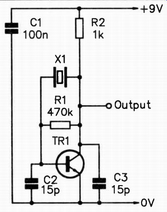
Fig. 2.1 A common crystal oscillator configuration
In practice it is quite possible that checking the output from the collector of TRI with such an instrument would cause the oscillator to cease operating. Capacitors C2 and C3 effectively form a capacitive tapping on the tuned circuit, which in this case is crystal X1 . These two capacitors do not need to be very accurately matched in order to obtain the desired circuit action with a phase inversion through the crystal so that positive feedback is obtained. However, a gross mismatch here and too little feedback to sustain oscillation will result. With this type of circuit the two capacitors are usually at values of around 10 u to 47 u, and the input capacitance of a simple a.c. voltmeter, especially if it does not use a probe type detector, could effectively boost the value of C2 by a few hundred percent.
The accepted way of obtaining a high input impedance at high frequencies with minimal shunt capacitance is to use an active probe. In other words, a probe unit that contains a buffer amplifier plus the rectifier and smoothing circuit. The output of the circuit is at d.c., and any stray capacitance in the output cable (which could be quite considerable) is of no real consequence. It is swamped by the very much higher value smoothing capacitance connected across the output of the rectifier and smoothing circuit. The lack of any cable at the input of a probe helps to keep the input capacitance to a minimum, and with an active type the isolation between the input and the rectifier and smoothing circuit helps to further minimize the input capacitance. Obviously the buffer amplifier will have a certain amount of input capacitance, but this need be no more than about 10p or so. While any input capacitance is undesirable, about 10 u is the minimum that can be readily achieved in practice, and is low enough to give excellent results in virtually all circumstances.
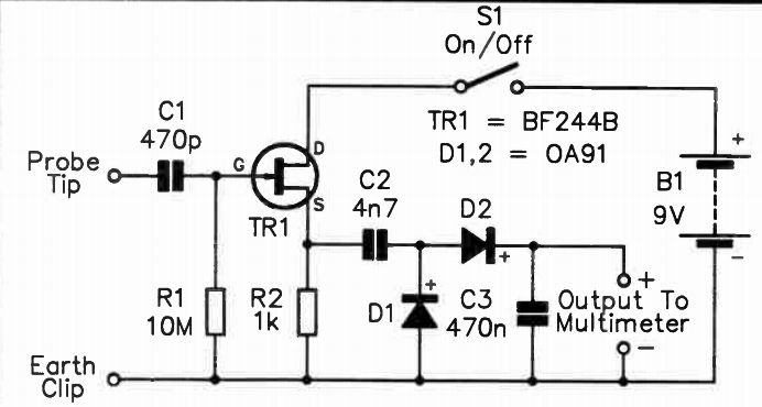
Fig. 2.2 The Active R. F. Probe circuit diagram
The Circuit
Figure 2.2 shows the circuit diagram for a simple but useful active r.f. probe. I built this for use with a 20k/volt analogue multimeter, but it should be usable with any multimeter, from low sensitivity analogue types through to digital and high impedance analogue instruments. The buffer amplifier is based on TRI, which is a J-fet device used in the common drain (or source follower) mode. This gives a little less than unity voltage gain, which is all we require in this application.
The advantage of a source follower stage is that it gives a high input resistance and low input capacitance. The input resistance is only fractionally less than the value of gate bias resistor R1, which is 10 megohms in this circuit. With the source follower mode there is no Miller Effect to multiply the basic input capacitance of the transistor, and this gives an input capacitance of only about 10 u.
The rectifier stage is a conventional twin diode half wave type, using germanium diodes to minimize the losses through the circuit. C3 is the smoothing capacitor. It would be unreasonable to expect good linearity from a circuit of this type, but it performs better in this respect than you might think.
The d.c. output voltage is approximately equal to the r.m.s. input voltage, and although the unit may not be suitable for precise measurements, it gives you a very good idea of the voltage level present at the input. The frequency response of the unit is quite good, and it should work well with input frequencies anywhere in the range 100kHz to 50MHz.
It is important to keep in mind that the unit is not intended for use with anything other than low voltage circuits, and that it will not function properly with input levels of more than a few volts peak-to-peak. Obviously these days most radio frequency circuits are low voltage semiconductor types, and relatively few electronics hobbyists have the need to test high voltage valve or semiconductor circuits which have high voltage supplies. If you should use the unit with circuits of this type there is a definite risk of damaging the semiconductors in the probe, especially TR1.
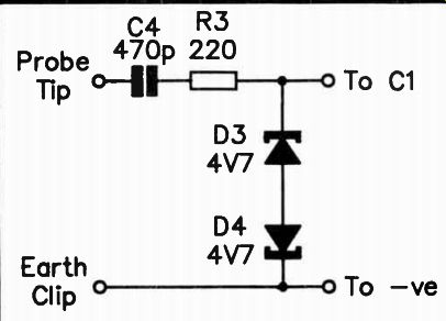
Fig. 2.3 A simple overload protection circuit for the R. F. probe
This risk can be minimized by adding the protection circuit of Figure 23. This consists of a series resistor plus zener diodes D1 and D2 to clip the input signal at approximately plus and minus 5.4 volts. Regardless of the input signal's polarity, one diode will act as a standard zener while the other will operate as a forward biased silicon diode. They provide approximate clipping levels of 4.7 and 0.7 volts respectively, giving a combined clipping level of plus and minus 5.4 volts.
I would not recommend fitting this protection circuit unless you are likely to use the unit on circuits that could provide dangerously high input voltages. The diodes are used in a series arrangement rather than a parallel one so as to minimize their capacitance, but they still give a substantial boost to the probe's input capacitance. This, together with input resistor R1, form a lowpass filter. This significantly impairs the high frequency performance of the circuit.
As always, unless you are completely sure you know what you are doing, you should not test any circuits which contain high voltages. Do not use a unit of this type on mains powered equipment that does not include an isolating transformer to give a chassis that is properly isolated from the mains supply.
To do so would be very dangerous indeed, and could prove fatal.
The circuit is very simple, and it is easily constructed using stripboard or a custom printed circuit board. Try to keep the layout compact so that the unit can be made as small as possible. The layout is not particularly critical, with no likelihood of the circuit breaking into oscillation. Designing a compact component layout is therefore quite straightforward.
Note that D1 and D2 are germanium diodes, and not the more familiar silicon variety. The practical importance of this is that they are more easily damaged by heat, and due care needs to be exercised when soldering them into circuit.
Mechanically, construction of any probe-type project requires a certain amount of ingenuity. You may be able to obtain a probe type case that will accommodate all the components including the battery, but it is quite possible that you will have to improvise using a small plastic case. Several cases of this type are available quite cheaply. A suggested form for the unit is shown in Figure 2.4. To keep the unit reasonably small and light the battery must be a low capacity type, such as one of the PP3 size batteries that are readily avail able. A low capacity battery is quite adequate as the current consumption of the circuit is only a few milliamps, and it is not necessary to use one of the expensive "high power" types.
The connection to the earth rail is made via an insulated lead about half a meter long and terminated in a crocodile clip. If the case is made from a soft plastic the small grommet in the exit hole for this lead is not essential, but will serve to give the unit a neater appearance. The metal prod part of the unit consists of a long M3 or 6BA bolt which is filed to the usual pointed tip. Ideally the bolt should be about 50 to 75 millimeters long, so that it is easy to poke the unit into the less accessible parts of the equipment under test. In practice you might have to settle for a somewhat shorter bolt, since longer ones do not seem to be stocked by electronic retailers. The bolt is fixed at one end of the unit using a suit able nut, and a solder-tag is fitted over the bolt inside the case.
This provides an easy means of making the connection to the probe tip.
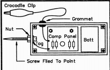
Fig.2.4 A suggested form of construction for probe- type projects
The on/off switch can be fitted on the case anywhere that will keep it out of the way when using the unit. Similarly, the exit hole for the output cable can be positioned anywhere that does not make the unit awkward to handle and use.
Probably in both cases the rear end of the unit is the best place for them. The on/off switch needs to be a very small type, and a sub-miniature toggle or slider type should be suitable.
The output cable does not need to be a screened type, and any twin cable should be suitable. As the output is at d.c. and a fairly low impedance it is quite in order to use a fairly long cable if desired.
It has to be emphasized that this is only a suggestion for the general make-up of the unit, and it is really a matter of making the most of the materials that are available to you. With a little ingenuity it should be possible to produce a reasonably professional finished unit. A fairly slimline case is preferable to a short stubby type, as a long slim case makes it easier to get the unit into the more inaccessible parts of electronic projects.
---------------
Components (Figs 2.2 and 2.3)
R1 10M watt 5%
R2 1k 1/4 watt 5%
R3 220 V4 watt 5%
C1 470p ceramic plate
C2 4n7 polyester
C3 470n polyester
C4 470p ceramic plate
TR1 BF244B
D1, D2 0A91 (2 off)
D3, D4 BZY88C4V7 4.7V 400mW zeners (2 off)
B1 9 volt (PP3 size)
S1 SPST miniature toggle
Case, circuit board, battery connector, etc.
----------------------
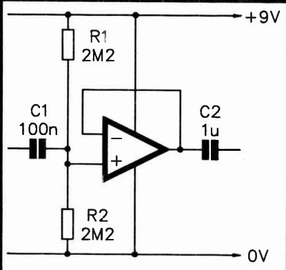
Fig. 2.5 The type of circuit that is prone to loading effects when making
d.c. voltage checks.
High Resistance Probe
The advantage of a d.c. voltmeter which has a very high input resistance was discussed in BP239, but to briefly recapitulate, the limitations of an ordinary analogue multimeter come to light when testing a high impedance circuit, such as the bias network in the buffer amplifier of Figure 2.5. This is a standard operational amplifier voltage follower circuit, where the voltage gain from the input to the output is unity. The circuit provides plenty of current gain though, with a low output impedance being produced from what in this case is an input impedance of about 1.1 megohms. R1 and R2 bias the input of the amplifier to approximately half the supply voltage, or about 4.5 volts in other words.
Measuring this voltage with a high impedance voltmeter, such as a digital multimeter having an input resistance of about 10 or 11 megohms, will give reasonably accurate results. The resistance of the multimeter is effectively shunted across R2, and will tend to pull the measured voltage below the 4.5 volt level, but the measured voltage should not be too far from the unloaded voltage at this point.
Making the same measurement with an ordinary 20k per volt multimeter will give a very different result. To measure a nominal potential of 4.5 volts it would seem to be reasonable to use the multimeter on its 5 volt d.c. range, but on this range it provides an input resistance of only 100k (5 x 20k = 100k). This would shunt R2 to such an extent that a very low reading indeed would be obtained. With an inexpensive 1-k per volt multimeter the resistance on the 5 volt d.c. range would only be 5k, which instead of giving nearly full scale deflection of the meter, would result in R2 being shunted to the point where the meter's needle would probably not be noticeably deflected!
The circuit of Figure 2.6 is for an input resistance booster that provides any multimeter with an input resistance of 20 megohms on its lower d.c. voltage ranges. The unit is not usable with input voltages of more than about 7 volts, but it is on low voltage readings that a high input resistance is likely to be greatest benefit. With modern semiconductor circuits virtually all voltage readings seem to be in the sub-ten volt range anyway.
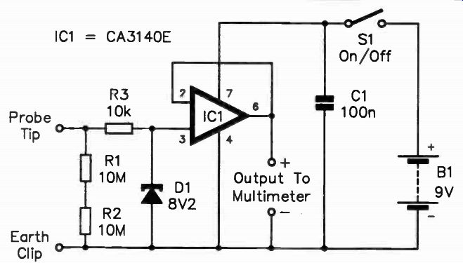
Figure 2.6
The circuit is basically just an operational amplifier used in the unity voltage gain non-inverting mode. R.3 and D1 provide protection against excessive input voltages. For positive input voltages D1 is reverse biased, and it acts as a conventional zener diode which avalanches to clip the input voltage at a little over 8 volts. With a negative input voltage D1 becomes forward biased, and clips the input signal at about -0.7 volts, like an ordinary forward biased silicon diode.
R1 and R2 are the input bias resistance for IC1, and they set the input resistance of the circuit. Two 10 megohm resistors in series obviously gives an input resistance of 20 megohms, but it is quite in order to use three or more of these resistors connected in series if desired. For instance, with five 10 megohm resistors an input resistance of some 50 megohms would be obtained, and accurate results should then be obtained even when testing very high impedance circuits.
IC1 is a CA3140E, which is a type that has an ultra-high input resistance due to its MOS input stage. It is also capable of operating in a circuit of this type without the need for dual balanced supplies. This is possible because the output stage can provide output voltages as low as a few millivolts. The use of an alternative operational amplifier in the IC1 position is not recommended. Very few other types have suitable characteristics.
Using a 9 volt supply the maximum output voltage from IC1 is about 8 volts, and it will be somewhat less than this as the battery nears exhaustion. The CA3140E can operate with supply voltages up to 36 volts, giving output voltages up to almost 35 volts. By using a higher supply potential it is there fore possible to extend the maximum input voltage that the unit can handle, but a supply voltage of more than about 18 volts (which can be provided by two PP3 size 9 volt batteries connected in series) are probably not very practical. Note that the voltage rating of D1 should be about one volt less than the nominal supply voltage.
The circuit is so simple that construction should pose few difficulties. Note though, that IC1 is a MOS input device that consequently requires the usual anti-static handling precautions. In particular, use an holder for this for this component, do not fit it onto the circuit board until construction is in other respects complete, and handle the pins as little as possible. The unit does not have to be built in probe form, but this probably represents the most practical approach. It is vulnerable to stray pick-up at the input due to its very high input impedance (especially if more than two input resistors are used), and because IC1 effectively provides half wave rectification. This will not matter if the unit is constructed as a probe, because a long positive test lead will then be avoided.
Pick-up in the short probe tip and wiring should be negligible.
If conventional test leads are used at the input it is quite likely that there will be a strong indication from the meter under no input conditions due to the stray pick-up of mains "hum" etc. One solution, and probably the best one, is to use oscilloscope style screened test leads. These can be expensive to buy ready-made, but do-it-yourself leads of this type can be produced reasonably cheaply. Another alternative would be to add a lowpass filter at the input of the unit, but this would slow up its response time slightly. Note that stray pick-up at the input does not matter when testing low impedance sources since the pick-up will drop to an insignificant level when the unit is connected to the test point. The same is not true when testing high impedance sources, and unless pick-up is kept down to an insignificant level the accuracy of voltage readings will be adversely affected.
The voltage range of the multimeter is, of course, unaltered by adding the impedance booster unit. However, bear in mind the maximum input voltage limitations mentioned previously.
Components (Fig.2.6)
R1 10M % watt 5% R2 10M 1/4 watt 5% R3 10k es watt 5% C1 100n ceramic disc D1 BZY88C8V2 8.2 volt 400mW zener diode IC1 CA3140E B1 9 volt (PP3 size)
S1 SPST miniature toggle Case, circuit board, 8 pin d.i.l. i.c. holder, battery connector, etc.
Dual Range Booster
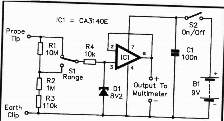
Fig.2.7 The circuit for the "improved" high resistance probe
Figure 2.7 shows the circuit diagram for an improved voltage probe unit. This is much the same as the original in that it consists of a voltage follower circuit with an overload protection circuit at the input. It is different in that the input bias resistors have been replaced with a simple two step switched attenuator (R1 to R3 plus S1). With S1 set so that R4 connects to the top end of R1 the unit functions in much the same way as the original circuit, but with a reduced input resistance of a little over 11 megohms. This input resistance is obviously still quite good, being comparable to analogue high impedance voltmeters and digital multimeters.
With S1 set to the opposite position the input attenuator reduces the input voltage by a factor of ten. Whereas previously the circuit had a maximum input voltage of around 7 to 8 volts, switching in the attenuator multiplies this to a more useful 75 to 80 volts maximum. It does this without the need for higher supply voltages, and requires the addition of only two extra components (S1 and a resistor) in comparison to the original circuit. Provided a miniature type is used for S1, there should be no difficulty in building the unit as a probe type tool. Note that the attenuator resistors must be close tolerance types in order to give accurate results on both ranges.
In use the unit is not greatly different to the original design.
However, bear in mind that when it is set to divide the input voltage by a factor of ten, the actual voltage reading is ten times the figure indicated by the multimeter.
Components (Fig. 2. 7)
R1 10M 0.6 watt 1%
R2 1M 0.6 watt 1%
R3 110k 0.6 watt 1%
R4 10k 1/4 watt 5%
C1 100n disc ceramic disc
D1 BZY88C8V2 8.2 volt
400mW zener diode
IC1 CA3140E
B1 9 volt (PP3 size)
S1 SPDT miniature toggle
S2 SPST miniature toggle
Case, circuit board, 8 pin d.i.l. i.e. holder, battery connector, etc.
Memory Probe
One of the most common problems when making voltage checks on circuit boards is the difficulty in holding the test prods in position while looking away to read the multimeter.
The small size and intricacy of modern circuits makes the job of keeping the test prods in place one that often requires all your concentration, even if you are able to clip the earth lead in place while the tests are made. You need to take due care when making voltage checks on awkward pieces of equipment-- it is all too easy to slip with the test prod and short circuit two adjacent contacts. Some lackadaisical testing could soon add a few more faults to the equipment being checked! A useful but rare feature which aids testing awkward equipment is a memory facility. This can operate in more than one way, but in its most simple form the multimeter holds the highest or last reading until a reset button is operated. If you are testing fixed voltages, you can simply connect the test prods to the test points, remove them, read the voltage from the multimeter, reset the instrument to zero, and move on to the next test. There is a slight flaw in this method of testing in that if the input voltage is slowly varying, this will not be apparent. You will simply get a reading equal to the highest input voltage while the test prods were connected to the circuit under test, or the last reading prior to them being removed, depending on the design of the multimeter.
This is not really a major drawback though, as in practice there are very few test voltages that vary slowly. Mostly they are either static or vary at a rate that is too high for the multi meter to cope with. However, it is probably not the technique to use if you are (say) checking for low frequency instability on supply lines, or anything where there is a definite possibility of a slowly fluctuating input voltage.
Although very few multimeters have any form of integral memory circuit, it is not difficult to add this feature using an external circuit. It will only function on the lower d.c. voltage ranges, but these are the ones that are most often used when making "dab it and see" style checks on circuit boards.
A very basic memory circuit can be provided using a passive circuit such as the one shown in Figure 2.8. This relies on the multimeter being a high input resistance type. When an input voltage is connected to the unit, C1 charges up to this input voltage, and when the input voltage is removed it discharges slowly into the high input resistance of the multimeter. The discharge process is very slow due to the high input resistance of the multimeter and the high value of C1. This gives you a few seconds to read the multimeter before the displayed voltage has time to "sag" significantly. Pressing reset button PBI rapidly discharges C1 through R1 so that a new reading can be taken. R1 provides current limiting so that sparking at PBI 's contacts is avoided, and it has a long operating life.
Although this circuit will work, it does have a couple of major deficiencies. One of these is simply that the readings are not held very well. Although the time constant of C1 and the 10 or 11 megohm input resistance of the multimeter is very long, tests made with a digital multimeter will clearly show the reading dropping on each update of the meter's display. This can be a bit confusing, making it difficult to take readings.
The second problem is the high value of C1. This will rapidly charge if the unit is fed from a low impedance source, but it could take several seconds or even minutes if the test point is at a high impedance. This could result in very low readings and misleading results being obtained. Also, connecting a high value capacitor to test points involves a slight risk of damaging components in the circuit. C1 could be made lower in value, but this would exacerbate the problem of "sagging" readings. C1 must be given a value that gives a goodcom promise between these two problems.
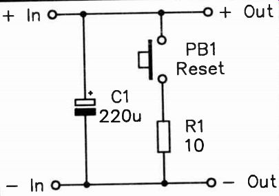
Figure 2.8
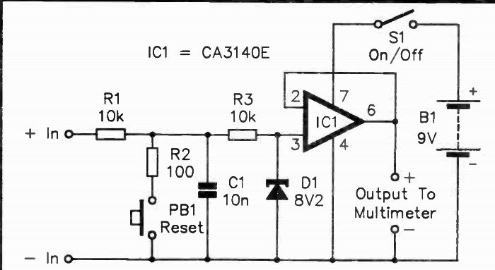
Fig.2.9 The circuit for the Active Memory Unit
Vastly superior results can be obtained using an active circuit, such as the one shown in Figure 2.9. The input part of the circuit is much the same as the passive circuit of Figure 2.8, and works in exactly the same way. It differs in that the value of the charge storage capacitor (C1) has been made very much lower in value at just 10 nanofarads. This is less than a thousandth of the original value, and it ensures that the input voltage quickly rises to the correct level even when the unit is fed from a high impedance voltage source.
The active part of the circuit is an operational amplifier used in the unity voltage gain non-inverting mode. This is much the same as the stage used in some of the previous circuits. It is possible to use such a low charge storage capacitor due to the MOS input stage of the CA3140E used in the IC1 position, and the ultra-high input resistance this provides.
The input resistance is about 1.5 million megohms, which ensures that there is no significant decrease in the charge on C1 over a period of a few seconds. In fact the main discharge path for C1 is likely to be through its own dielectric, and the use of a good quality plastic foil type is recommended. The low value of C1 means that there is little risk of it causing any damage to components in the equipment under test. However, R1 provides current limiting that ensures there is absolutely no risk of any charge or discharge currents of sufficient magnitude to damage anything in the test circuit.
D1 provides overload and reverse polarity input protection, as in some of the circuits described previously. Obviously this component provides an additional discharge path for C1, and could degrade the performance of the circuit. In practice this does not seem to be a problem though, and at voltages reasonably well below the avalanche point a zener diode seems to exhibit a very high resistance indeed.
This is another very simple circuit that should be very easy to construct. It could easily be built as a probe, and in use this would probably be the most convenient form for the unit.
Bear in mind that the maximum output voltage is about one volt less than the supply voltage. Higher supply voltages can be used in order to increase the maximum possible output voltage, but the 36 volt maximum permissible supply potential for the CA3140E must not be exceeded.
Components (Fig. 2.9)
R 1 10k 1/4 watt 5%
R2 100R 1 / 4 watt 5%
R3 10k 1 / 4 watt 5%
C1 10n polyester or polycarbonate
D1 BZY88C8V2 8.2 volt 400mW zener diode
IC1 CA3140E
B1 9 volt (PP3 size)
S1 SPST miniature toggle
PB1 Push to make - release to break
Case, circuit board, 8 pin d.i.l. i.c. holder, battery connector, etc.
A.C. Voltage Booster
Although multimeters have few major deficiencies, few are very good at making very low voltage measurements. This is one respect in which digital instruments are generally much better than analogue types, apart from a few high quality analogue multimeters. It is perhaps not so much a problem for d.c. voltage measurements, where most multimeters are some what better, and very low d.c. voltage measurements are not something that need to be made very often anyway. The problem is usually more acute when making measurements on audio gear where it is often necessary to make low a.c. voltage checks. Few multimeters, especially analogue types, offer full scale values of less than about 5 or 10 volts. This does not provide particularly good resolution, and makes it impossible to measure potentials of just a few millivolts. In some cases even inputs of a few hundred millivolts can not be measured with reasonable accuracy.
If you have a digital multimeter with 0.1999 volt a.c. and d.c. voltage ranges, then you are fortunate in that you can accurately measure quite small a.c. and d.c. voltages, with a resolution of some 100 microvolts (0.1 millivolts). This is adequate for most audio testing, but the frequency response limitations of most digital multimeters have to be taken into account. With an upper limit to the frequency response of typically about 500 hertz, gain testing etc. can be undertaken provided a suitable test frequency is chosen. Noise measurement and most frequency response testing are not practical
propositions using such an instrument. Also, the lack of logarithmic decibel scaling on a digital multimeter makes it less than ideal for much audio testing.
As pointed out in BP239, some audio tests can be under taken by ensuring that the output level is high enough to properly drive a multimeter set to a low a.c. voltage range. This is a bit risky though, in that there is a real possibility of overloading the equipment under test and obtaining misleading results.
Not all equipment can provide a high enough output level to permit this approach to be used successfully. More reliable results and a greater range of tests can be undertaken if the multimeter is preceded by an amplifier to boost its sensitivity.
This method is particularly useful if it is applied to an analogue multimeter which has an a.c. voltage range with a full scale value of only about one volt, a bandwidth of 20kHz or more, and decibel scales. Adding a simple and inexpensive amplifier to a multimeter of this type provides you with a setup that is capable of the type of testing that would otherwise require an expensive a.c. millivolt meter or an oscilloscope.
The Circuit
Figure 2.10 shows the circuit diagram for a simple a.c. voltage booster circuit. The input stage is a simple unity gain buffer amplifier that provides an input impedance of over one meg ohm (less at high frequencies due to the inevitable input capacitance). This high input impedance alone gives a definite advantage over using an unaided analogue multi meter for low a.c. voltage checks. Most analogue multimeters have a sensitivity of 20k per volt on the d.c. voltage ranges, but the sensitivity is often much lower on the a.c. voltage ranges. It is usually in the region of 5 to 10k per volt. This gives rather low input impedances on the low a.c. voltage ranges (only 10k on a 2 volt a.c. voltage range with a sensitivity of 5k per volt for instance).
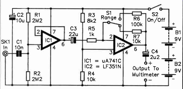
Fig.2.10 The A. C. Voltage Booster circuit diagram
The voltage amplification is provided by IC2 which is an operational amplifier used in the standard inverting mode. It has two switched feedback resistors (R6 and R7) which provide voltage gains of 40dB (one hundred times) and 20dB (ten times) respectively. With the multimeter switched to (say) the 2.5 volt a.c. range this would give full scale values of 25 millivolts and 250 millivolts r.m.s. Note that these are the full scale values, and that it should be possible to measure voltages of around one millivolt reasonably accurately. The theoretical bandwidth of the amplifier is about 400kHz in the X10 mode, and 40kHz in the X100 mode. In practice the bandwidth might be slightly less than these figures, but even so, the unit still encompasses more than the full audio range.
The limiting factor might be the bandwidth of the multimeter, but most analogue types seem to have a frequency response that extends at least as far as the 20kHz upper limit of the audio spectrum.
Power is obtained from two 9 volt batteries wired in series to give an 18 volt supply. This enables an output of up to about 5 volts r.m.s. to be obtained. In order to obtain accurate results right up to the full scale value, the multimeter must therefore be switched to a range having a full scale value of 5 volts or less. Most multimeters have a suitable range, but a few have a 10 volt range as their lowest a.c. voltage type. With instruments of this kind they should either be used at output voltages of less than 5 volts, or a higher supply voltage should be used. The maximum permissible supply potential is 36 volts, which gives a maximum unclipped output voltage of around 11 volts r.m.s. If the multimeter has a 1 or 1.5 volt a.c. voltage range, then it will almost certainly be possible to obtain satisfactory results with the unit powered from a single 9 volt battery. The current consumption is only a few milliamps, and PP3 size 9 volt batteries are adequate as the power source.
Constructing this unit is a little more difficult than building the circuits described previously in this Section. The unit is still pretty simple, but as it has a high input impedance and a fair amount of voltage gain it is necessary to be reasonably careful with the component layout if instability is to be avoided. As the input and output of the circuit are out-of phase, problems with stray feedback are minimized, but reasonable care with the layout still needs to be taken. In order to avoid problems with stray pick-up of mains "hum" etc., it is a good idea to fit the unit in a metal case earthed to the negative supply rail.
The test leads must be of the screened variety so as to minimize stray pick-up and to minimize the risk of problem with instability. Obviously there is no need to use a screened lead to connect the output of the unit to the multimeter in order to avoid stray pick-up. The signal in the output cable is at a relatively high level and low impedance. However, using screened output lead is probably a good idea as it keeps down any radiation of the output signal to an insignificant level which aids the avoidance of problems due to stray feedback
Components (Fig.2.10)
R1 2M2 1 / 4 watt 5%
R2 2M2 1 / 4 watt 5%
R3 8k2 1 / 4 watt 5%
R4 10k Vs watt 5%
R5 1 k 0.6 watt 1%
R6 100k 0.6 watt 1%
R7 10k 0.6 watt 1%
C1 10n polyester
C2 10µ 40V elect
C3 22µ 25V elect
C4 21./2 63V elect
IC1 pA741C
IC2 LF351N
SK1 3.5min jack socket or similar
S1 SPDT miniature toggle
S2 SPST miniature toggle
B1 9 volt (PP3 size)
B2 9 volt (PP3 size)
Case, circuit board, 8 pin d.i.l. i.c. holder (2 off), battery connector (2 off), etc.
Gain Estimation
In use the system is suitable for many applications that would conventionally be the province of an a.c. millivoltmeter or an oscilloscope. These include such things as gain measurement, noise measurement, and frequency response testing.
Some types of audio testing are covered towards the end of BP239, including frequency response testing and audio output power measurement. These can both be checked using the setup described here, but the higher sensitivity achieved with the amplifier added enables measurements to be made at lower levels than would otherwise be possible.
The measurement of voltage gain is an important part of audio testing, since a loss of gain in an audio circuit is a common result of a fault. Quickly tracking down the stage which has inadequate voltage gain can obviously make finding the exact problem much easier and faster. The basic method of checking is to inject an audio signal at a suitable level into the input of the equipment, and to then check the signal level at various points in the circuit. If there is a total or very substantial loss of signal at some point in the unit, then locating the faulty stage is not likely to be too difficult. You could, for example, make tests at the input and output of every stage in the circuit working from the input to the output. When a point in the circuit with an inadequate level is located, the fault is in the immediate vicinity of that point, and is probably just prior to it.
Very often the problem is not a total break in the signal path, or even a large loss of gain. The loss of gain is frequently only around 10dB (about 3 times) to 30dB (about 30 times). When testing for these lower levels of signal loss you need to be able to judge the sort of voltage gain that each stage should be providing. The problem might be obvious, because a stage of amplification might be providing losses rather than gain. On the other hand the problem could be a less obvious one with, for example, an amplifier that should be providing 50dB of voltage gain actually providing only about 20dB of gain.
Transistors have three basic amplifying modes, and the basic circuits for each of these are shown in Figure 2.11. The configuration shown in (a) is the common collector mode, which is better known as the "emitter follower" mode. It is easy to spot this type of amplifier as it is the only one which has the output signal coming from the emitter. There is no difficulty in working out the voltage gain of an emitter follower -- it is always fractionally less than unity. This type of amplifier is used as an impedance converter to match a high impedance source to a low impedance load.
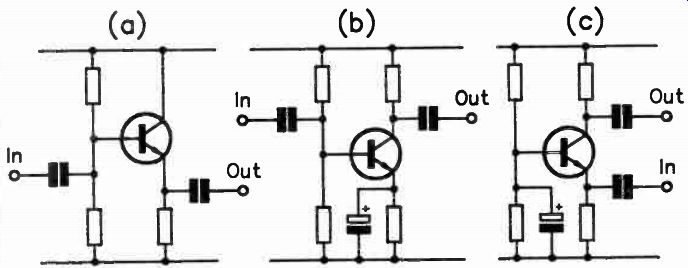
Fig.2.11 The three transistor amplifying modes.
The configuration of (b) is the common emitter mode, and is probably the one that is used most frequently. The voltage gain of this mode is quite high, but the precise figure varies considerably depending on the component values and the current gain of the transistor. With low gain transistors the voltage gain is still likely to be in excess of ten times, and with high gain types such as the BC107 and BC547 series the voltage gain would normally be over one hundred times.
Modern common emitter stages often use a more simple form of biasing which has the emitter connected direct to the earth rail and the two base bias resistors replaced with a resistor connected between the base and collector terminals.
This provides a certain amount of negative feedback, but does not massively reduce the voltage gain of the circuit. What does produce a large loss of gain is the unbypassed emitter resistor which is sometimes included to provide local negative feedback. In some cases there is a single resistor and no bypass capacitor in the emitter circuit. In other cases there are two resistors with a bypass capacitor connected across one of them.
As a quick "rule of thumb", the voltage gain is approximately equal to the value of the collector load resistor divided by that of the unbypassed emitter resistance. This gives quite accurate results unless the unbypassed emitter resistance is quite low in value (about 100 ohms or less). The problem is that there is effectively some emitter resistance within the transistor that must be added to the external resistance. As this internal resistance is typically only about 25 ohms, it is often not large enough to affect the calculation significantly.
However, if the emitter resistance is quite low in value, the voltage gain of the stage will be slightly lower than the method of calculation described above would suggest.
The configuration of (c) is the common base mode. This is little used in audio circuits, but it is sometimes used as part of the so-called "long-tailed pair" configuration. This is basically just an emitter follower stage directly driving a common base amplifier. The input impedance of this type of stage is low, and it is sometimes used as the input stage of a circuit that requires a low input impedance (such as certain types of microphone preamplifier). There is a moderate …
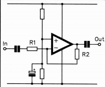
Fig.2.12 The inverting amplifier configuration.
Voltage gain = R2/R 1.
… amount of voltage gain through this type of circuit, which provides an action that is a bit like a step-up transformer.
Accurately judging the voltage gain of audio amplifier stages that are based on operational amplifiers is a somewhat easier task than dealing with discrete transistor based circuits.
There are two basic modes of operation, which are the inverting mode of Figure 2.12, and the non-inverting mode of Figure 2.13. In the inverting mode the non-inverting input is biased to about the mid-supply level by a potential divider circuit. A negative feedback circuit comprised of two resistors connects between the output, the inverting input, and the input. These are resistors R1 and R2 in Figure 2.12, and their value sets the voltage gain of the amplifier. It is delightfully simple to calculate the voltage gain. Simply divide the value of R2 by that of R1.
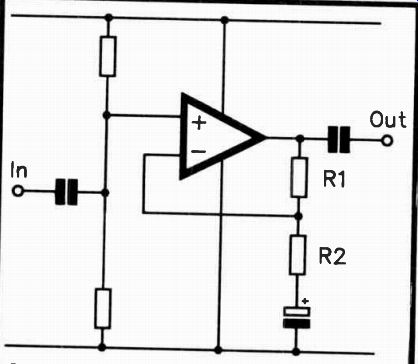
Fig. 2.13 The non inverting amplifier configuration.
Voltage gain = (R1 + R2)/R2.
The non-inverting circuit is similar, but the input signal is coupled to the non-inverting input. The feedback network connects between the output, the inverting input, and the earth rail. The mathematics of the circuit's voltage gain are a bit different with this configuration. The voltage gain is equal to the values of R1 and R2 divided by the value of R2.
If the ratio of R1 to R2 is quite high, simply dividing R1 by R2 will give a reasonably accurate answer.
Both configurations are frequently used with capacitors in the feedback circuit in order to give a contoured frequency response. This technique is often used in tone controls and R.I.A.A. preamplifiers for instance. This complicates matters as in order to work out the voltage gain you must first calculate or look-up the reactance of each capacitor at the test frequency, then work out the effective feedback resistances.
It is probably more practical to simply check that the appropriate type of frequency response is being produced, and to assume that the stages are functioning correctly if nothing seems to be amiss with the frequency response.
Stages based on audio amplifier integrated circuits can cause problems when trying to "guesstimate" voltage gains.
Some or all the negative feedback components may be within the integrated circuit. The popular LM380N audio power amplifier device is a good example of such a component. In these cases the relevant data book or data sheet should supply the typical voltage gain of the device, which is 34dB (50 times) in the case of the LM380N. Some audio integrated circuits have one feedback resistor within the device and the other one as an external component, so that the designer can exercise some control over the voltage gain of the device. For instance, some audio power amplifiers in the TBA800 series use this system, with an internal resistor of about 6k in value connected between the output and the inverting input of the amplifier. Provided you can find the value of the feedback resistor in the data on the device, or perhaps graphs showing voltage gain versus external feedback resistor value, you should be able to work out the correct voltage gain for the circuit.
One final point to watch when gain testing is that there is no overall negative feedback loop which will affect the voltage gain through each stage. With power amplifiers and discrete preamplifier circuits, it is not unusual to have several stages connected in series, with overall negative feedback to set the closed loop voltage gain accurately at the required figure.
Stages which provide unity voltage gain will still do so with overall negative feedback applied, but those that provide voltage gain will produce less than normal due to the feedback.
This presents no real problem provided you spot the overall feedback and take it into account. In fact a lack of gain through one stage will probably be partially counteracted by increased gain through another stage, making the lack of gain in the faulty stage stand out more clearly.
Current Tracing
Tests on circuit boards tend to be in the form of voltage rather than current tests, since the latter can only be made if a break is made in the signal path so that the meter can be connected into it. There are actually some expensive pieces of equipment which measure current flow using a Hall Effect device to measure the magnetic field around the wire which carries the current, but these are quite expensive and are probably not a practical proposition for the home constructor. There is a more simple alternative, and although it is quite crude by comparison it can nevertheless provide some quite useful results.
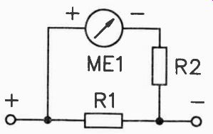
Fig.2.14 Basic current measuring circuit
This alternative system is really just a variation on the standard current meter arrangement. The basic current measuring setup is shown in Figure 2.14. It consists of a resistor through which the current to be measured must pass (R1), plus a voltmeter to measure the voltage developed across the resistor (MEI and R2). Ohm's Law dictates that the voltage across the resistor is proportional to the current flowing through it. Although the meter is actually measuring the voltage across the resistor, it can therefore be calibrated directly in terms of current flow.
In a simple current tracing setup a dual test prod with the prods separated by a few millimeters is used. This is connected to a length of copper track on the printed circuit board, or onto a component leadout wire. In effect, the piece of copper track or leadout wire between the two prods acts as the resistor of the current meter. By measuring the voltage developed across the two prods a good idea of the current flow through the track or wire is obtained.
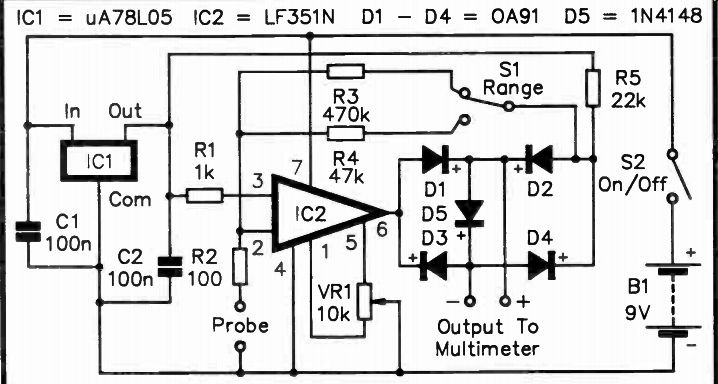
Fig.2.15 The current tracer circuit diagram.
The problem with this arrangement is that the resistance through a short piece of copper track or leadout wire is extremely low. Even with a fairly high current of an amp or two, the voltage obtained is unlikely to be more than a milli volt. With small currents the voltage obtained is likely to be no more than a few microvolts, and could be even less. Even using a digital multimeter on its 0.1999 volt range (which has a resolution of 100 microvolts) it is unlikely that usable results would be obtained. An ordinary 20k per volt analogue multi meter plus a high gain d.c. amplifier on the other hand, will work very well in this application. Figure 2.15 shows the circuit diagram for an add-on amplifier that enables an analogue multimeter to be used as a current tracer.
This is basically just a conventional full-wave precision rectifier of the type often used in audio millivoltmeter circuits.
It is not essential to have a circuit that will respond to inputs of either polarity, but it is a definite advantage. In this application you can not simply connect one test prod to the earth rail and dab the other one onto various points in the circuit, thus ensuring an input of the correct polarity. The tracking of many modern printed circuit boards is so convoluted that the polarity of the signal carried by each track might not be immediately obvious. The only slight drawback of this method is that you can not determine the polarity of the current flow using the unit, although it would seem unlikely that it would ever be necessary to do so. An advantage of using a dual polarity circuit is that the unit should be able to detect a.c. signals as well as d.c. types, but the limited upper frequency response means that it will only operate efficiently at frequencies of a few hundred hertz or less.
The circuit is a form of operational amplifier inverting mode amplifier. IC1 is a small monolithic voltage regulator that provides a stable bias potential of 5 volts to the non inverting input of IC2. It also provides what is effectively the mid-supply earth rail. The meter circuit is driven from between this pseudo-earth and the output of the amplifier by way of a bridge rectifier (D1 to D4) and series resistor R5. R2 plus R3 or R4 forms the negative feedback network, and controls the voltage gain of the circuit. Having two switched feedback resistors provides the unit with two sensitivities, with R3 offering approximately ten times more gain than R4. As the rectifier circuit is included in the feedback loop it tends to counteract the non-linearity through the diodes, giving better results. Germanium diodes are used for D1 to D4 because their lower voltage drop makes them more suitable for this application than the more common silicon diodes such as the 1N4148.
D5 is used to protect the meter against severe overloads. If a strong output signal should be produced, D5 will become forward biased and will clip the output voltage at about 0.65 volts. This should prevent any damage to the multimeter, which should be switched to the 50 microamp d.c. current range. VR1 is the offset-null control. With a theoretically perfect operational amplifier this control is unnecessary. Real operational amplifiers tend to fall short of theoretical perfection in a number of ways, and one result of this is small voltage differences between the inputs and the output. These are multiplied by the closed loop voltage gain of the amplifier, and with the high gain that has to be used in this application the result is a strong positive deflection of the meter under standby conditions. VR1 enables the offset voltage to be trimmed out, and the meter to be properly zeroed under quiescent conditions.
Construction of the unit should once again be quite simple.
Although the circuit has a substantial amount of voltage gain, its low input impedance plus the fact that the input and output are out-of-phase means that instability is not a major problem. VR1 can be an ordinary panel control, or a preset resistor on the main circuit board. Using a panel mounted control has the advantage that it can easily be re-trimmed from time to time should it prove necessary to do so (which it probably will). If this component is a preset resistor it should be a multi-turn type as the resolution of many ordinary preset resistors is inadequate for this application. Using a multi-turn "trimpot" has the advantage of making the critical adjustment of VR1 much easier.
There are two approaches to the test prods for this unit.
One is simply to use a pair of ordinary multimeter type test prods, which you place a few millimeters apart on the track or wire being tested. This is the method I prefer as it is simple, and it permits the test prods to be positioned as far apart as the length of track or lead permits. This gives the best possible input signal to the unit. The disadvantage is that by using an inconsistent track or wire length it becomes more difficult to interpret results. You must learn to take into account the length of track or wire used when assessing results. This is not too difficult, since the effective sensitivity of the unit is proportional to the length of track or wire used. The second method is to fix the two prods together so that the metal tips are a few millimeters apart. This brings the advantage of a consistent gap between the prods, and only one hand is needed to manipulate them. The drawback is that a quite small gap must be used if the unit is to be usable on any track or wire.
This gives a relatively low input signal, and effectively reduces the sensitivity of the unit.
When first switched on it is unlikely that any offset will be apparent, and the meter should be properly zeroed. This is due to the fact that with no input signal connected to an inverting mode operational amplifier circuit its effective voltage gain is unity. If you place a short circuit across the test prods, this will place the circuit under normal operating conditions, and a strong deflection of the meter will probably result. VR1 is adjusted to accurately zero the meter, and it will almost certainly need to be adjusted very carefully in order to achieve this. Carry out this adjustment with the unit on its more sensitive range (S1 set to switch R3 into circuit), as it is on this range that there is the largest offset.
The only way to master a unit of this type is to experiment with it on a circuit that is operating correctly, and where you know the approximate current running through each track.
This will give you a good idea of what to expect when testing faulty equipment. In many cases the current flows in faulty areas of equipment are so far removed from the correct figures that there is no difficulty in detecting them. The sensitivity of the unit should be adequate, but low currents may not give a significant deflection of the meter. You can obtain increased voltage gain by making R2 lower in value.
This reduces the input impedance of the unit, but as the source impedance is so low this should not result in significant loading of the test voltage. The main problem is that the higher the sensitivity is made, the more difficult it becomes to zero the meter using VR1, and the more prone the circuit becomes to drifting of the bias levels. It is perhaps worth while experimenting with lower values for R2 to see if this gives acceptable stability, and it is worthwhile using a lower value if results are acceptable in this respect.
Components (Fig.2.1.5)
R1 1k 1 / 4 watt 5%
R2 100R 1 / 4 watt 5%
R3 470k 1 / 4 watt 5%
R4 47k 1 / 4 watt 5%
R5 22k 1/4 watt 5%
VR1 10k lin potentiometer or multi-turn preset
C1 100n disc ceramic
C2 100n disc ceramic
IC1 µA78L05 +5 volt 100mA regulator
IC2 LF351
D1 0A91
D2 0A91
D3 0A91
D4 0A91
D5 1N4148
S1 SPDT miniature toggle
S2 SPST miniature toggle
B1 9 volt (PP3 size)
Case, circuit board, 8 pin d.i.l.
Lc. holder, battery connector, control knob, etc.
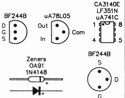
Fig.2.16 Leadout and pinout details (I.C. top views, transistor base views).