Fiber optics have for many years now been hailed as the way of things to come, but have so far had only limited impact. Some of the problems involved with fiber optic communications have proved to be difficult and time consuming to crack, especially the problems of high attenuation over a given length of cable, and the relatively high cost of effective fiber optic cables. Fiber optics are now beginning to have a greater impact on the electronics world, and it is an area which offers a lot of scope for the electronics experimenter.
Advantages
Electronic signals have for many years been sent quite successfully over ordinary "hard -wire" links, or via radio links of one kind or another, and on the face of it there is no way of justifying all the expense and effort that has so far gone into fiber optic development. In fact fiber optic links, whether for something like high quality audio or video links over long distances, or control short distances, can have definite advantages.
One big advantage of fiber optic links is their total immunity to pick up of electrical interference. Ordinary wired links can be designed to minimize this problem, but it is difficult to totally eliminate it, and doing so can be extremely expensive indeed.
Obviously the non-electrical nature of a fiber optic cable makes electrical interference irrelevant, except in that pick up of interference in the electronics at the receiver is still possible. However, effective screening of the receiver circuit is unlikely to prove to be particularly difficult.
In a similar vein, high speed signals sent down an ordinary electrical cable tend to radiate electrical interference which can disrupt radio and television reception in the vicinity. Again, a fiber optic cable it is totally free from electrical radiation, and although the transmitter unit might generate a certain amount of radio frequency radiation, it is quite easy to contain it using simple screening techniques.
Stemming from this lack of radiation, in a system having several cables running side-by-side there is no problem with crosstalk.
Obviously light could leak from cable to another, but fiber optic cables are enclosed in an opaque outer sleeving which in practice results in no significant leakage, and certainly nothing like enough to give any crosstalk problems. This lack of radiated signal makes fiber optic links relatively secure and virtually tap-proof.
Other advantages include no fire hazard problems as there are no electrical signals to cause sparking or the possibility of excessive currents flowing and causing overheating of the cable.
There is electrical isolation through the link so that problems with earth loops can not occur. With suitable transmitting and receiving circuits it is possible for fiber optic links to have very large bandwidths. Wide bandwidth links can be produced using coaxial electrical cables, but modern optic cables generally have lower losses than coaxial types in wide bandwidth applications.
Optic cables are usually narrow and light, as well as being resistant to weather and many chemicals. This often enables them to be used easily in hostile environments or awkward situations where electrical cables, particularly coaxial types, might be less well suited.
Despite their advantages fiber optic cables have yet to achieve really widespread use. The obvious drawback is that electrical signals can not be feed direct to an optical cable, and in many cases the expense and difficulty of the necessary encoder and decoder circuits could not be justified. We are nowhere near the stage where electrical and electronic equipment could be economically wired up with fiber optic cables, and they are generally only used where distances of at least several meters are involved, or freedom from electrical interference is of crucial importance.
An important point to bear in mind when using optical fibers is that they normally have a recommended minimum radius, and if they are bent through a tighter curve than this it is quite likely that the cable will sustain serious damage at that point, rendering it useless. The "minimum bend" radius as it is usually termed in the data sheets, is generally between about 50 and 80 millimeters.
There is a popular electronics joke about tying a knot in a mains lead to make it more difficult for the electricity to run down the cable, and thus reduce the power fed the device served by the cable. The effect of curves in a mains cable may be insignificant, but with fiber optic cables curves (even ones that are inadequate to damage the cable) can impede the propagation of the light waves and cause significantly increased losses.
Cable Basics
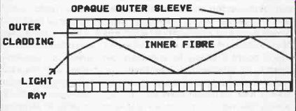
Fig. 1. Cross section through an optical fiber showing high order propagation.
Although many people seem to be under the impression that a fiber optic cable just consists of a glass filament contained in an opaque outer sleeving, things are actually a little more complicated than this. These days the glass filament is more likely to be polymer than glass, and the usual arrangement is as outlined in Figure 1 where there is a central core having a high refractive index and an outer cladding of lower refractive index. Refraction where the inner filament and the outer cladding meet enables light to travel down the cable by effectively bouncing from wall to wall down the cable. It is this bouncing effect that enables the cable to operate as a light guide, taking the Bight around corners and bends. The angle at which the light is reflected depends on the characteristics of the cable and the entry angle of the light. In Figure 1 the light ray is subjected to "high order mode" propagation, but light entering at a shallower angle would bounce off the wall of the cable at a much shallower angle, and would consequently travel much further per bounce. This is termed "low order mode" propagation. The practical importance of these two modes is that light travelling through the cable in the high order mode has to travel significantly further than light which is propagated in the low order mode. This smears signals sent down the cable, and limits the maximum frequency that can be accommodated. This is only of significance in very wide bandwidth links though, and with the types that we will consider here it is not a practical consideration. So called "Single mode" cables are designed so that only one mode of propagation is supported, but it is not necessary to use a cable of this type with the relatively narrow bandwidth systems described in this guide.
There is an alternative type of cable called "graded index" cable (as opposed to the "stepped index" type described previously).
This is actually quite similar to the stepped index cable, but there is a gradual change from a high refractive index at the centre of the cable to a lower value close to the sleeving. This results in the light travelling down the cable in much the same way as described previously, but with the light taking a curved route (as in Figure 2) rather than being propagated in straight lines.
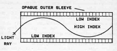
Fig. 2. Propagation through a graded index fiber optic cable
The standard size for optical fiber cables is 2.2 millimeters in overall diameter with a fiber diameter of 1 millimeter. There are various connectors available for use with this size of cable, as well as a few devices which connect to suitably prepared cables. A typical connector system has a "plug" which is fitted onto the end of the cable and secures it to the "socket" which mounts on the circuit board and has an aperture into which the photocell (emitter or detector) fits. The analogy with electrical plugs and sockets is perhaps not a very good one in that an optical connector system does not usually carry the light signal and does not usually contain any optics - it is just used to keep the cable in place and aligned with the photocells. The photocells with integral connectors that I have encountered have all had a sort of screw terminal into which the cable is fully pushed home, after which it is secured by tightening the terminal.
An important factor to keep in mind is the light wavelength at which the emitter has its peak output. Ideally the receiving device should have a peak response at a matching frequency, and it must certainly have reasonably high sensitivity at this frequency. Also bear in mind that the cable will only have a limited bandwidth, and it must provide reasonably low losses at the output wavelength of the emitter. Most opto devices intended for fiber optic applications operate at peak efficiency in the infrared or nearly infrared part of the spectrum. Most cables are quite efficient in the visible light part of the spectrum, and some are designed to peak at the centre of the visible light range. The majority have optimum efficiency in the infrared part of the spectrum though.
Fiber optic cables are usually supplied with unprepared ends, and may be extremely inefficient unless the ends are properly cut and polished. In my experience the cable will give good results if it is cut at right angles using a sharp modeling knife, cutting through it cleanly in a single movement. A fine file can be used to polish the ends of a cable, but if it has been cut properly in the first place this is unlikely to significantly increase the level of light transmission. It is important that the cut is made perpendicular to the cable, as an angled cut will give reduced efficiency, and will tend to shift the optimum light entry angle off its normal end-on angle.
What can be very much more difficult than cutting the cable is stripping off the outer sleeving from the end of a cable. This is often necessary in order to fit the cable into a connector, and like stripping sleeving from an ordinary wire lead, it is important not to nick the inner part of the cable. With electrical leads this is mainly to avoid the severe physical weakening effect this has on the cable, but this in not a major factor with an optic cable except in an extreme case. It is more a problem of the efficiency of the cable being greatly reduced unless due care not to damage the fiber is taken.
Ordinary wire strippers can sometimes be quite effective with fiber optic cables, but most cable/stripper combinations do not seem to give good results. A method which often works well is to make a slit along the sleeving over the entire length of the piece that is to be removed. This requires a very sharp knife, with due care being taken not to cut too deep and not to slip and cut yourself or the worktop (the small round shape of fiber optic cables makes them a little awkward to deal with). Once this cut has been made it is quite easy to peel back the piece of sleeving and trim it off with the knife.
Audio Link
A good starting point for someone wishing to experiment with fiber optic communications is to build an audio link. In its most basic form this would consist of a simple amplitude modulation system with the brightness of the transmitting LED being varied in sympathy with the amplitude of the audio input signal. This would give corresponding variations in the leakage current through the receiving photocell, which would be converted to a varying voltage by adding a load resistor in series with the photocell. This signal would be amplified and would provide the audio output signal.
In practice this simple method has its drawbacks, and the main one is simply a lack of linearity through the photocells. This lack of linearity is directly reflected in the distortion performance of the link which is consequently very poor. Readers with the appropriate technical knowledge might like to experiment with a system of this type, but it is not a topic that will be perused further in this guide.
A system which generally gives better results is a frequency modulation type, which is essentially the same as the system used for high quality VHF radio broadcasts. However, in this case we are dealing with a carrier frequency of around 100kHz rather than the 100MHz of a band II radio transmission. A system of this type can be quite simple, and the block diagram of Figure 3 shows the basic arrangement for a simplex (single way) link of this type.
The transmitter is based on a voltage controlled oscillator (VCO), and as its name implies, the output frequency of this circuit can be varied by means of a control voltage. This voltage is the audio input signal in the present application, and as the signal voltage rises and falls, so does the VCO's output frequency. A lowpass filter is used to process the audio input signal before it is fed to the VCO, and this is to prevent heterodyne "whistles" from being generated due to beat notes between the VCO and any high frequency input signals. In most cases the input signal will only span the audio range, but there could be distortion products at higher frequencies, and there is also the possibility of radio signals being picked up in the wiring and reacting with the VCO signal or harmonics on the VCO's output signal.
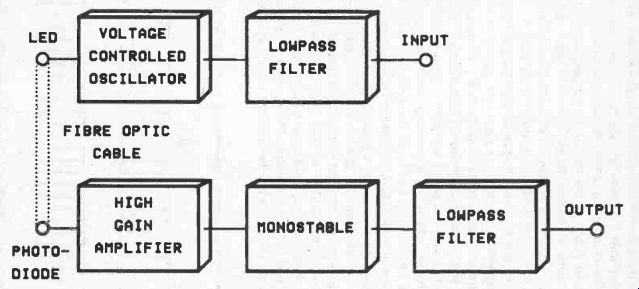
Fig. 3. Block diagram for a simple fiber optic audio
The output of the VCO drives the emitting device, and with simple links of the type described here this device is a light emitting diode (LED) of some kind. In order to get good results it is generally necessary to drive the LED at a substantial current, and a buffer amplifier will therefore normally be needed between the output of the VCO and the LED.
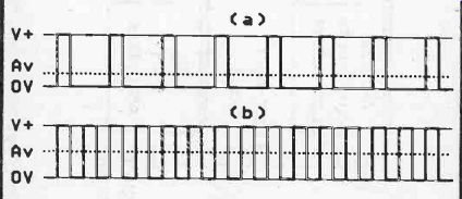
Fig. 4. In the output waveform of (a) the average voltage is one quarter of
the supply voltage. In (b) the frequency has been doubled, and so has the average
output voltage.
At the receiving end of the system a photo-diode is used as the detector (or possibly a photo -transistor would be used here), and even with efficient coupling of light through the system the output from the photo detector is unlikely to be very large. In fact it would by typically only a few millivolts peak to peak. A high gain amplifier is consequently needed in order to boost the signal to a high enough level to drive the next stage of the unit.
This next stage is a monostable multivibrator and it must be of the non-retriggerable variety. It therefore provides an output pulse of a duration that is controlled by the C-R timing network and is totally independent of the input pulse duration. This gives a simple but effective frequency to voltage conversion, and the waveforms shown in Figure 4 help to explain the way in which this operates. In Figure 4(a) the input frequency is such that the output from the monostable has a 1 to 3 mark-space ratio, and the output is in the high state for 25% of the time. The average output voltage (as indicated by the dotted line) is consequently one quarter of the high state output voltage. In Figure 4(b) the input frequency has been doubled so that there are twice as many output pulses in a given period of time, and the mark space ratio is 1 to 1. This gives an average output voltage of half the high state output voltage, and twice the level of the previous example. In other words, the monostable is not just giving a frequency to voltage conversion, but it is also providing a linear characteristic.
The output from the monostable does not itself constitute an audio frequency signal, but a lowpass filter is all that is needed in order to smooth the pulsed output into a normal audio signal. The main drawback of this very simple form of frequency to voltage conversion is that a high degree of attenuation (preferably 80dB or more) is needed at the minimum output frequency of the VCO in order to give a low ripple output. On the other hand, this system is very simple and reliable in other respects, and with modern circuits it is not difficult to produce an output filter having a suitably sharp cut off characteristic. A small amount of residual carrier signal on the output would probably not be a serious problem anyway, since the carrier is always at frequencies well outside the audio range, and any breakthrough at the output will therefore be inaudible.
This may seem to be an unnecessarily complicated way of doing things, but it does have its advantages, particularly with regard to the linearity through the system. The main point to note in this respect is that linearity through the LED and the photo -diode is totally irrelevant as they are used as switches and not in a linear mode. In theory the system has perfect linearity, but in practice a certain amount of distortion will be generated, mainly due to non linearity in the VCO's control characteristic, but other stages of the system can also contribute significant distortion levels. Even so, a simple system can achieve a total harmonic distortion level of under 1% together with a high signal to noise ratio.
Transmitter Circuit
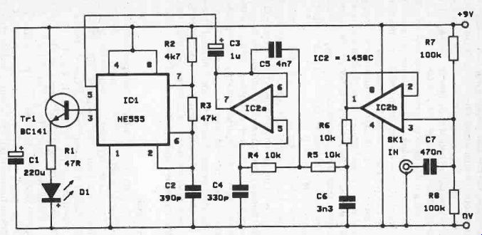
Fig. 5. The circuit diagram for the fiber optic audio transmitter.
The full circuit diagram of the transmitter unit appears in Figure 5.
There are various integrated circuits that are suitable as the VCO, as well as numerous discrete component configurations, but for an inexpensive system the popular NE555 is the obvious choice, and although it is a very cheap device, it offers a quite reasonable standard of performance. It can be frequency modulated by coupling the input signal to pm 5, which connects to the potential divider that sets the 1/3 V+ and 2/3 V+ switching thresholds of the device. In effect the upper threshold is raised and lowered so that the time taken for timing capacitor C2 to oscillate between the two levels can be raised and lowered. This does not give the standard VCO effect in that increased input voltage gives reduced output frequency, and reduced input voltage results in boosted output frequency. This is of no real importance in practice, and the system stills works perfectly, but with a phase inversion of the signal through the overall system.
Tr1 is an emitter follower buffer stage which provides the high drive current needed by the LED (Dl). The NE555 can actually provide quite high output currents, but it seems to be possible to set the LED current more accurately and reliably with the buffer amplifier added. R1 sets the LED current at about 40 milliamps, but as the LED is switched off for approximately 50% of the time this results in an average LED current of only about 20 milliamps.
The output current can be raised or lowered by altering the value of R1 if desired, and the output current is inversely proportional to the value of this component (e.g. Hiving its value doubles the output current). Bear in mind that most LEDs can take a maximum average current of only about 50 to 100 milliamps though, and obtaining long range using a high output power is not a practical proposition.
The input filter is a conventional 18dB per octave type based on IC2a. The cut off frequency is at about 10kHz or so, and the system does not achieve the full audio bandwidth of about 20kHz.
The centre carrier frequency is about 30kHz, and the minimum carrier frequency is close to the 20kHz upper limit of the audio range. This, on the face of it, does not give much scope for using a higher filter cut off frequency so as to give the full audio bandwidth. By making R4 to R6 (and the equivalent resistors in the filter at the receiver) 5k6 in value, the system can in fact accommodate the full audio spectrum, but it is also necessary to reduce the value of C2 to 180pF in order to raise the carrier frequency to an adequate figure (about 60kHz) to accommodate the extra bandwidth. C4 in the receiver circuit should also be reduced in value to 180pF incidentally.
This increase in bandwidth leaves the system more exposed to problems with heterodynes and general noise, and the photocells may be less effective at the higher frequency range. Good results should be obtained provided a strong signal is present at the receiver, but under marginal conditions results may be degraded to an unacceptable level. It is therefore advisable to use the values specified in the components list unless the full audio bandwidth is really needed.
IC2b operates as an input buffer stage which ensures that the filter is fed from a suitably low source impedance, and it gives the unit a reasonably high input impedance of about 50k.
=============
Components for Fiber Optic Transmitter (Fig. 5)
Resistors (all Vs watt 5%)
R1 47R R2 4k7 R3 47k R4 10k R5 10k R6 10k R7 100k R8 100k
Capacitors
C1 220µ 10V elect
C2 390pF ceramic plate
C3 1 u 63V elect
C4 330p ceramic plate
C5 4n7 polyester layer
C6 3n3 polyester layer
C7 470n polyester layer
Semiconductors
IC1 NE555
IC2 1458C
Tr1 BC141
D1 see text
Miscellaneous
SK1 3.5mm jack socket
Circuit board, case, battery, etc.
========
Receiver Circuit
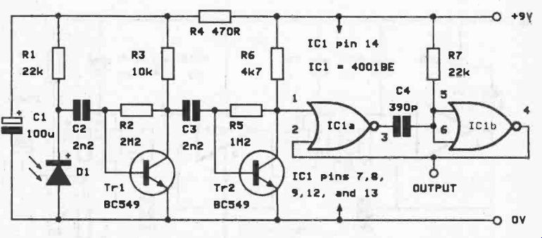
Fig. 6. The circuit diagram of the amplifier and mono-stable stages of the
fiber optic receiver
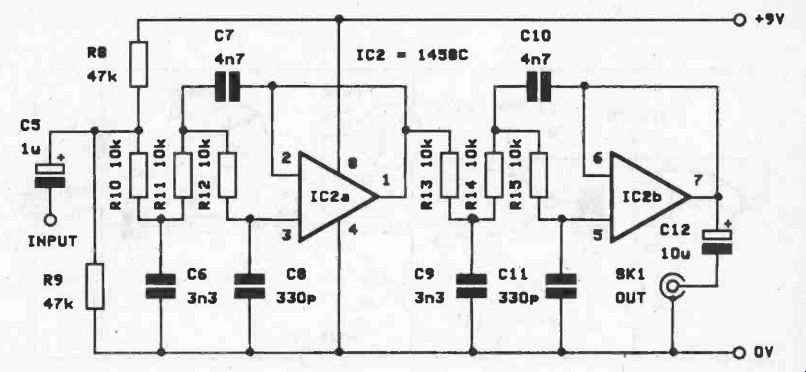
Fig. 7. The circuit diagram for the filter stages of the fiber optic receiver.
The main receiver circuit diagram appears in Figure 6, but the output filter circuit is shown separately in Figure 7.
D1 is the detector diode, and it operates in the reverse bias mode where its leakage resistance provides a sort of light dependent resistance action. R1 is its load resistor, and C2 couples the output from the detector circuit to the input of the amplifier. This is a two stage capacitively coupled design with both stages operating in the common emitter mode: This gives a high overall voltage gain of more than 80dB. Provided a reasonably strong input signal is present, this gives a sufficiently high output voltage swing at the collector of Tr2 to drive the monostable multivibrator.
The latter is a conventional CMOS type formed from two 2 input NOR gates (IC1a and IC1b) with C4 and R7 as the timing components. The other two gates of IC1 are unused, but their inputs are tied to earth in order to prevent spurious operation of these gates.
Turning our attention to Figure 7, this is basically just two third order (18dB per octave) filters of the type used in the transmitter unit. They are connected in series so as to provide a total of six poles and an overall attenuation rate of 36dB per octave. This gives around 100dB of attenuation of the carrier signal at its lowest frequency, and an output signal which has a reasonably low carrier content.
The system will handle input voltages of up to 1 volt RMS or so without producing serious distortion, and there is slightly less than unity voltage gain through the system.
Components for Fiber Optic Receiver (Figs. 6 and 7)
Resistors (all 1/4 watt 5%):
R1 22k R2 2M2 R3 10k R4 470R R5 1M2 R6 4k7 R7 22k R8 47k R9 47k R10 to R15 10k (6 off)
Capacitors
C1 100µ10V elect
C2 2n2 polyester layer
C3 2n2 polyester layer
C4 390p ceramic plate
C5 1 µ 63V elect
C6 3n3 polyester layer
C7 4n7 polyester layer
C8 330pF ceramic plate
C9 3n3 polyester layer
C10 4n7 polyester layer
C11 330pF ceramic plate
C12 10µ 25V elect
Semiconductors
IC1 4001BE
IC2 1458C
Tr1 BC549
Tr2 BC549
D1 see text
Miscellaneous
SK1 3.5mm jack socket
Circuit board, case, battery, etc.
Components for Data Link Receiver (Figs. 6 and 11)
Resistors (all 1/4 watt 5%)
R1 22k R2 2M2 R3 10k R4 470R R5 1M2 R6 4k7 R7 22k R8 to R13 5k6 (6 off)
Potentiometer
VR1 22k sub -min hor preset
Capacitors
C1 100µ 10V elect
C2 2n2 polyester layer
C3 2n2 polyester layer
C4 390p ceramic plate
C5 3n3 polyester layer
C6 4n7 polyester layer
C7 330p ceramic plate
C8 3n3 polyester layer
C9 4n7 polyester layer
C10 330p ceramic plate
Semiconductors
IC1 4001BE
IC2 1458C
IC3 CA3140E Tr1
Tr2 BC549 (2 off)
D1 See text
Miscellaneous
SK1 25 way D connector
Case, circuit board, wire, etc.
Construction
Construction of the unit is mainly quite simple and straight forward, and from the electrical point of view the main point to watch is that due care is taken with the layout of the amplifier in the receiver unit. This has high gain, a fairly wide bandwidth, and an input and output that are in-phase. Any stray feedback of significant proportions from the output to the input of the circuit is therefore likely to cause instability. Use a layout that keeps these two points in the circuit as well isolated from one another as possible. IC1 is a CMOS device and it consequently requires the standard antistatic handling precautions to be observed. The main precautions are to use a socket for the device, and not to plug it into circuit until the unit is in all other respects finished. Until it is time for IC1 to be plugged into the holder it should be left in its antistatic packaging (which is usually conductive foam or a plastic tube). Try to avoid touching the pins as far as possible and handle the device as little as possible when fitting it. Also avoid having any obvious sources of static electricity in the vicinity when dealing with this component.
From the mechanical stand -point the only real complication is the fiber optic connections. The prototype was constructed using a Motorola MFOE71 emitter and an MFOD71 diode detector.
These are very convenient in use as they both have screw terminal type fixings for standard 2.2/1 millimeter fiber optic cable. With devices of this type about 4 millimeters of sleeving should be removed from each end of the cable so that the ends can be fully pushed home into the devices. The terminals should only be tightened just enough to hold the cable firmly in place. These components are intended for mounting directly on a printed circuit board, and a small nut and bolt (6BA or M3 bolts about 6 millimeters long are suitable) can be used to fix each one more securely to its board. Do not worry if the light output from the emitter seems rather dim - its peak output is at about 820nm, which is well into the infrared spectrum. Most of its output is therefore invisible to you (but there will be some output in the visible red part of the spectrum). With these two devices a range of about 20 meters should be easily attained using any reasonable quality fiber optic cable (i.e. a type having an attenuation level of about 1.2dB per meter). Of course, with the emitter having most of its output in the infrared part of the spectrum, the cable must be a type which provides good efficiency at the relevant wavelengths.
The circuits should work well with any other emitters and photo -diodes intended for use with fiber optic cables. In most cases though, it will be necessary to obtain suitable connectors separately. In fact it is quite possible to use opto devices that are not specifically intended for fiber optic use, and a connector system can be improvised without too much difficulty. In the case of the connectors it is just a matter of using a bit of ingenuity and whatever suitable materials are to hand. I have found that grommets and heat-shrink sleeving are quite useful as the basis of a home-made optic connector system.
Any light emitting diode can be used to direct light down a fiber optic cable, but the best devices are something like a hundred times more effective than the worst. Ordinary 3 millimeter and 5 millimeter diameter LEDs do not seem to give a high enough output for even short range use, and the "high-brightness" types are much better. Best of all are the "ultra -bright" devices which often achieve their high output levels, at least in part, by using a lens which gives a very narrow beam of light. Obviously for the present application there is no disadvantage in this. 5 millimeter diameter LEDs seem to be better than the 3 millimeter types which generally have an output intensity which is only about half that of the larger devices. Some 5 millimeter diameter LEDs currently available have an output intensity of typically 250mcd at a drive current of 20 milliamps, and they are not particularly expensive.
Virtually any photodiode is suitable as the detector, but it must obviously have good efficiency at the wavelength at which the LED has its peak output, and it must be a type which physically enables the light output from the cable to be efficiently coupled into it. Something like a large area infrared photo -diode offers less than the ideal physical characteristics, with the fiber optic cable providing only a narrow light source.
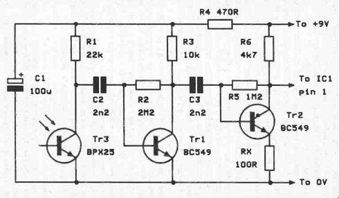
Fig. 8. The modified section of the receiver circuit to permit use of a photo-transistor.
Photo-transistors having built-in lenses (such as the BPX25 and TIL81) can provide quite good results, but with these the gain of the amplifier might be excessive. The problem is really one of stray feedback to the base of the photo -transistor causing instability, and the component layout of the unit needs to be carefully designed in order to prevent problems arising, or the gain of the amplifier must be reduced slightly.
Figure 8 shows the way in which a photo -transistor can be used in the receiver. The input circuit and amplifier are much the same as before, but the detector diode has been replaced by photo-transistor Tr3. The collector to emitter leakage current is being used as a light dependent resistance with the base terminal of the transistor being left unconnected. Resistor "RX" has been added in the emitter circuit of Tr2 to introduce local negative feedback and reduce the gain of the amplifier slightly. If necessary the value of RX can be increased slightly so as to introduce more feedback and further reduce the gain of the amplifier, or if the component layout permits, the emitter of Tr2 can be connected direct to the 0 volt supply rail so that full gain is provided. Although a BPX25 is specified for the Tr3 position, a TIL81 and a BPY62 were tried in the circuit and were also found to work perfectly well.
For good results at low cost the best solution is probably to use an ultra-bright LED as the emitter and a photo -transistor as the detector, in conjunction with home-made fiber optic terminations. Using a set up of this type I found a range of 20 meters could be easily achieved, and although I did not try the equipment over greater distances, a much larger range than 20 meters would almost certainly be possible.
As it stands the unit provides only monophonic operation and a one way link. By using two complete systems with a twin fiber optic cable (or two separate cables running side by side) either stereo operation or a two way link can be provided.
Data Link
When connecting computers together via RS232C or the similar (and compatible) RS423 serial interfaces there can be problems with earth loops and with radio frequency interference being radiated. A fiber optic data link avoids both problems, and it is not difficult to produce a system that can handle standard serial signals at any baud rate up to the normal maximum of 19200 baud.
One way of tackling the problem would be to use the serial input signal to directly gate the transmitting LED on and off. A detector circuit and DC amplifier would then be used at the receiver to detect the pulses of light and convert them back into a serial signal at the appropriate voltage levels.
There is a severe drawback with this method in that the output from the detector circuit would almost certainly be at a very low level unless quite expensive emitter and detector devices were to be used. This would make it difficult to obtain good reliability and long term stability. An advantage of this direct approach is that it enables quite high baud rates to be handled, and even without resorting to any particularly exotic photocells a baud rate of 200k baud or more could probably be accommodated. With the right devices baud rates of several megabaud or even several tens of megabaud can be handled. However, as normal home and business computers do not support baud rates of more than 19.2k baud, this high speed capability is largely of academic interest for most users.
Better results can be obtained using a frequency modulation system, much like the one in the audio link just described.
However, with a computer data link there are only two signal levels to contend with, and the carrier wave is therefore switched between two frequencies rather than being swept up and down in frequency. This is actually the same system that is used in modems in order to provide computer communications via the telephone system, but where modems use frequencies ranging from a few hundred Hertz to a couple of kilohertz, in this case much higher frequencies can be utilized. The practical significance of this is that the maximum baud rate is not limited to 300 or 1200 baud as in the case of modems, and the system described here can comfortably handle 19200 baud.
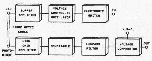
Fig. 9. Block diagram for a simple fiber optic data link for RS232C serial
signals
The block diagram of Figure 9 outlines the arrangement used in a simple tone encoder/decoder optical data link, and this has obvious similarities to the audio link described previously.
A voltage controlled oscillator again forms the basis of the transmitter, with its output driving the transmitting LED (via a buffer stage if high output currents are required). The input signal is in the form of a logic signal, but RS232C links do not use normal 0 volt and 5 volt logic levels. The nominal signal levels are plus and minus 12 volts, but the minimum requirement is only plus and minus 3 volts, and the maximum (unloaded) output level is plus and minus 24 volts. With RS423 serial interfaces the signal voltages are generally somewhat lower at about plus and minus 5 volts, which is within the minimum requirements of the RS232C system, and provides compatibility with it. In this case the input signal is used to drive an electronic switch which it closes when the signal goes high. The switch closing reduces the input voltage to the VCO and takes the output frequency higher.
At the receiver there is again a high gain amplifier, a monostable, and a lowpass filter. These provide an output voltage which switches higher and lower in sympathy with the RS232C input signal, but the switching speed is too low and the voltage levels are wrong, and this signal can not directly drive an RS232C or RS423 input. A voltage comparator is all that is needed to provide the speeding up and level conversion so that a fully compatible RS232C and RS423 output signal is produced. With serial signals the mark space ratio of the signal is all important, and any "smearing" of the signal is likely to give corrupted data.
The reference voltage fed to the comparator must be accurately set half way between the two peak levels of the input signal so that the mark space ratio of the original signal is accurately. preserved.
Transmitter Circuit The full circuit diagram for the data link transmitter appears in Figure 10.
Like the audio link transmitter, this one is based on an NE555 operating in the standard astable configuration, and the LED is driven by way of an emitter follower buffer stage. R2, R3, and R5 are used to pull the control voltage input of IC1 slightly higher than its normal level, and this gives a quiescent output frequency of about 40kHz. Tr1 operates as the electronic switch, and it is a simple common emitter type having R1 to provide current limiting and Dl to give reverse voltage protection. With the input signal at the -12 volt level Tr1 remains cut off, and the output frequency stays at its 40kHz quiescent level. However, when the input signal goes to the 12 volt level Tr1 becomes biased hard into conduction. It then pulls the voltage at the junction of R2 - R3 - R5 down to little more than 0 volts, and consequently pulls the control voltage fed to IC1 much lower. This sets the output frequency to a somewhat higher figure of around 60kHz. The circuit is designed to operate from a 5 volt supply as most computers are capable of supplying +5 volts at the sort of currents _involved here (the circuit draws about 35 milliamps of supply current).
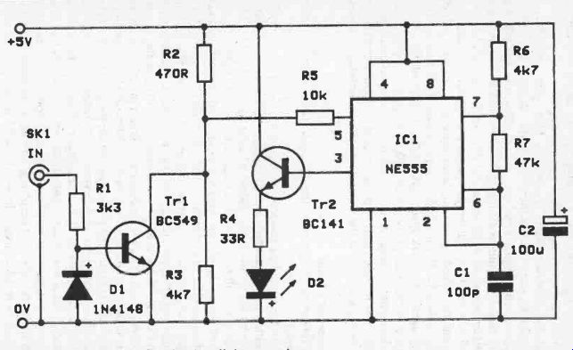
Fig. 10. The circuit diagram for the data link transmitter
Components for Data Link Transmitter (Fig. 10)
Resistors (all 1/4 watt 5%)
R1 3k3 R2 470R R3 4k7 R4 33R R5 10k R6 4k7 R7 47k
Capacitors C1
- C2 100pF ceramic plate 100µ 10V elect
Semiconductors
IC1 NE555 Tr1 BC549 Tr2 BC141 D1 1N4148 D2 see text
Miscellaneous
SK1 25 way D connector
Circuit board, case, battery, etc.
Receiver Circuit
The detector, amplifier, and monostable circuits used in the audio link are also used in the data link receiver. No modifications at all are required to the circuit, but note that the output signal must be taken from pin 3 of IC1 and not from pin 4 (as was previously the case). This gives a complement of the normal output of the monostable, so that the output voltage from the lowpass filter is at a low level when the carrier is at its higher frequency, and a high level when the carrier is at the lower frequency. The voltage comparator gives an inversion which gives the correct high frequency to high output voltage and low carrier frequency to low output voltage relationship, so that there is no inversion through the system as a whole.
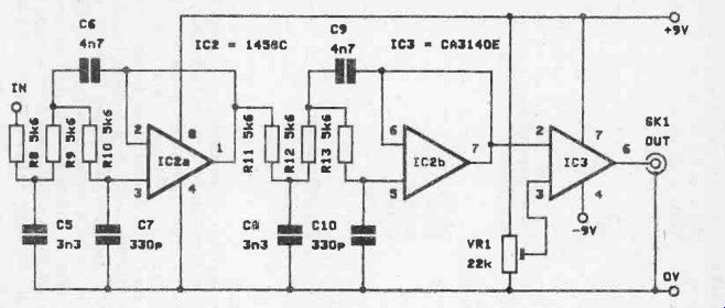
Fig. 11. The filter and comparator circuits of the fiber optic data link receiver
Figure 11 shows the filter and comparator circuits. The filter is very much the same as the one used in the audio link, but in this case it must use DC coupling, and the cut off frequency must be somewhat higher. The maximum switching frequency is produced when the input signal is alternate "marks" and "spaces", and with a 19200 baud signal is 9.6kHz. The filter's cut off frequency is about double this figure, thus enabling the maximum 19200 baud rate to be comfortably handled by the system. The circuit still provides around .40dB of attenuation at the lower carrier frequency so that there is a reasonably low ripple content on the output signal.
IC3 is an operational amplifier which operates here as the voltage comparator. VR1 is connected as a potential divider across the supply rails and it provides the reference voltage for the comparator. Originally a resistor was connected between pins 3 and 6 of IC3 to provide positive feedback and a trigger action rather than a simple comparator action. However, the output of IC3 seems to switch cleanly from one state to the other without the aid of any hysteresis, and so this resistor has been omitted from the final design.
Note that IC3 is powered from a -9 volt supply and not from the 0 volt rail. This is done in order to give output levels of around -9 volts and +7.5 volts, which are sufficient to drive RS232C and RS423 interfaces properly. In practice it may well be found that the circuit will drive serial interfaces properly even if pin 4 of IC3 is simply wired to the 0 volt supply rail and the negative supply is omitted, provided only a short connecting cable is used between SK1 and the computer (or whatever). Correct operation can not be guaranteed unless a negative supply is used.
What is often the most convenient way of obtaining a negative supply rail is to derive it from the positive supply using a DC to DC converter. A circuit of this type is shown in Figure 12, and it is based on an ICL7660 integrated circuit which is specifically designed for this purpose.
The ICL7660 is basically a high frequency audio oscillator driving a DPDT electronic switch. The action of the circuit is to first connect C1 across the positive input supply where it becomes charged up, and then to connect it across the negative output supply where it discharges, but it is connected across the output with the appropriate polarity so that the non-earthy output is negative of the earth rail. This process is repeated several thousand times per second with C1 transferring power from the input supply to the output, and C2 smoothing the pulsed output signal to give a reasonably low ripple final supply output. Dl is a protection diode.
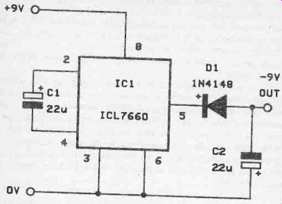
Fig. 12. A simple negative supply generator circuit There are inevitably losses
through the electronic switches, and the output voltage is not equal to the
positive input voltage. The ICL7660 is quite efficient though, and the loaded
output voltage should only be about 1 volt less than the input voltage, which
is quite sufficient for the present application. Note that the maximum input
voltage for the ICL7660 is only 10 volts, and that a nominal 9 volt supply
therefore represents about the maximum safe supply voltage for the device.
Construction
The constructional notes for the audio fiber optic link apply equally to this system, except that in this case there is a second MOS device in the form of IC3, and the usual antistatic handling precautions also need to be observed when dealing with this component.
In the components lists 25 way D connectors have been specified as the input and output sockets, and these are the standard RS232C connector.
Many computers that have a serial interface do not use this type of connector though, and it may well be more convenient to use something like a 5 way DIN socket, or whatever type of connector happens to match your computer equipment. The manual or manuals for your equipment should give connection details for the serial ports. The "signal ground" and "data output" terminals are coupled to the transmitter, while the receiver drives the "signal ground" and "data input" terminals.
As described here the system provides only simplex operation without any handshake lines being implemented. For full duplex operation it would be necessary to build up two systems with a separate fiber optic cable for each one, so that there would be a separate system to carry the signals in each direction. Hand-shaking could be implemented by adding further links, but with serial systems that operate over more than very short distances it is unusual to bother with hardware handshaking. Normally the system is designed in such a way that the receiving equipment can keep up with a continuous data flow so that handshaking is unnecessary, or in some cases a form of software handshaking is adopted.
Adjustment
If suitable test gear is available, couple a squarewave signal of around 10kHz in frequency and a few volts peak to peak in amplitude to the input of the system. Use an oscilloscope to monitor the output waveform of the receiver, and adjust VR1 for a 1 to 1 mark-space ratio.
Without the aid of test equipment it is still possible to set up VR1 properly. The computer connected to the transmitter unit should be set up to repeatedly send a short group of characters at the highest baud rate the system will ever need to handle. The receiving terminal should be set up so that it displays received characters on the television or monitor screen. There should be a narrow range of settings which provide uncorrupted data at the receiving terminal, and VR1 is merely adjusted to roughly the centre of this range of settings.
The system is capable of handling any standard baud rate or word format, but the transmitting and receiving terminals must, of course, be set up to use the same baud rate and word format.
Apart from use as a serial data link the system has other possible uses. It is effectively DC coupled, and it can be used for remote control purposes if used with suitable input and output circuitry. Where a number of control lines are required, one solution would be to use several of these links in parallel. However, if more than a couple of lines are needed it would probably be better to use a single link with a UART (universal asynchronous transmitter/receiver) at each end of the system. The UART at the transmitter would be used to convert parallel data to serial data suitable for transmission through the link. The UART at the receiver would then convert the serial data back into parallel form. Up to eight lines could be carried by a single link using this system.
Light Pen
Although using a fiber optic cable in a light pen application might seem to be just a gimmick with only disadvantages and nothing definite in its favor, a fiber optic light pen is really a perfectly practical device. It is admittedly likely to be more costly than a conventional equivalent, but the cost of a short piece of fiber optic cable plus a suitable detector and optic connector system is not that large these days.
In its favor this method has simplicity of the "pen" construction and excellent screen resolution. Construction of the so called "pen" (i.e. the part which is held and aimed at the screen) is very simple since it does not need to contain any electronics, not even the photocell. The latter is contained in the case which holds the main electronics, and the light from the screen is guided to it by the fiber optic cable. If desired, an old pen case or something of this nature can be fitted at the end of the fiber optic cable in order to make it easier to hold, but it is not needed for any other reason.
The high degree of precision is obtained due to the narrow filament diameter of the cable which, as explained previously, is normally only some 1 millimeter in diameter. This, coupled with the fact that only light running almost parallel to the end of the cable will be efficiently coupled through it, makes the unit sensitive over only a very small area of the screen. This is obviously important if the light pen is to be used in drawing or other applications which require a high degree of resolution, although for something like menu selection it is of somewhat less significance. It is possible to obtain a high degree of resolution from a conventional light pen, but the built-in lenses of most photocells are not good enough to give really good results.
Improved performance consequently requires the use of an extra lens or something like a short but narrow piece of tubing to reduce the pen's angle of view. Using a fiber optic cable is almost certainly a better and easier way of doing things, as well as giving the project more interest value.
Fundamentals
Although many people seem to imagine that a light pen produces a light beam, it does of course detect light. When used in the most basic way the pen simply indicates whether the pen is aimed at a bright or dark part of the screen, rather than indicating an absolute position on the screen. A basic set up of this type is rather limited in scope and is a bit crude even for simple applications such as menu selection. On the other hand, it can be made to operate in conjunction with virtually any spare digital input on the computer.
Many computers have a special light pen input (usually on the expansion bus or a joystick port rather than at a special light pen port), and with these it is normally possible for the pen to indicate an absolute screen position, although not necessarily with any great precision or reliability. This depends on the design of the light pen hardware within the computer, and some are very much better than others. Also, the degree of precision is affected by the resolution of the computer's screen, and again, some machines are capable of much higher resolution than others.
It is possible for the light pen to indicate a particular screen position due to the way in which the display is produced. It operates in the general manner shown in Figure 13, and the picture is produced by a line scanning process. In Figure 13 the solid lines represent the lines scanned by the electron beam of the cathode ray tube (CRT) while it is activated. The dotted lines show the flyback paths, and during these periods the beam is blanked so that nothing is produced on the screen. The general action then, is for the beam to start in the top left hand corner of the screen, and to scan across and down the screen in a series of lines until it reaches the bottom right hand corner. The beam is then taken back to the top left hand corner, and the process is repeated indefinitely.
The beam is not simply switched full on all the time it is being scanned along a line, but is modulated in intensity so that the brightness of the line is varied. In practice there are hundreds of lines and they are closely packed together. At normal viewing distances the individual lines can not be seen, and they merge together to form the picture. Close inspection of most monitor or ...
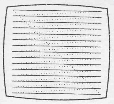
Fig. 13. A computer display is generated using a scanning process (solid lines
represent the scans and the dotted lines are the flyback periods)
... television screens will reveal the lines though. With a normal television picture a system called "interlacing" is used, and this means having every other line scanned on the first pass over the screen, with the remaining lines being scanned on the next pass. Fifty scans of the screen are completed each second, but as two scans are needed per complete picture, there are only twenty five pictures per second. The point of interlacing is that it gives a more flicker-free picture.
If a light pen is held over a part of the screen that is reasonably bright, this will not result in its output triggering to the appropriate logic state and staying there until the pen is removed from the screen. The scanning process produces what is really a spot of light that is moved across and down the screen, and although the scanning action is too fast for the human eye to perceive, the light pen will detect the spot as it passes through its field of view. The light pen therefore produces an output signal that consists of fifty brief output pulses per second.
The video circuits of the computer produce the timing signals that control the scanning. Some extra hardware in the video circuits is used to provide a counter of some kind, and a typical arrangement would be to have a counter that is incremented each time a new line scan is started, and another which runs from (say) 0 to 255 as each line scan progresses. The pulses from the light pen are used to halt the count, and the numbers in the counters then give X and Y co-ordinates which indicate the screen position of the light pen. Note that the counters do not always give X and Y co-ordinates directly, and with the popular 6845 video controller chip for example, the numbers in the two light pen registers form one large number and not separate co-ordinates. In this case the number increases as the spot progresses from the top left hand corner of the screen to the bottom right hand corner. Obviously, some simple mathematical manipulation is all that is needed to convert the single large number into separate X and Y co ordinates, but the exact formula needed will vary from one screen mode to another.
Circuit Operation
Light pens can be extremely simple, as can be seen by referring to the circuit diagram of the fiber optic light pen which appears in Figure 14.
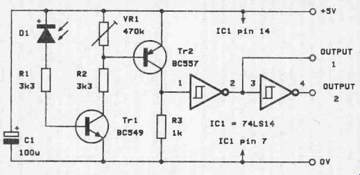
Fig. 14. The circuit diagram for the fiber optic light pen.
D1 is the photocell and is a photo -diode operated in the reverse bias mode. On the prototype an MFOD71 diode was used in the D1 position, and this is a good choice as it has a built-in fiber optic cable connector (of the screw terminal type) and reasonable sensitivity at visible light wavelengths. However, any photo-diode which offers good sensitivity over the visible light spectrum and can be efficiently coupled to a fiber optic cable should be equally suitable. The current flow through Dl when the spot of light is detected is likely to be quite low at no more than a few microamps, and possibly not even as much as this. Its output is therefore coupled to a high gain DC coupled amplifier which uses both Tr1 and Tr2 as common emitter stages. VR1 enables the sensitivity of the pen to be set at a suitable level. The output pulses at the collector of Tr2 are fed to two inverting Schmitt triggers wired in series, and these provide normal 5 volt logic compatible (antiphase) outputs. Output 1 is normally high and pulses low when the spot of light is detected - Output 2 is normally low and pulses high when the light spot is detected. The manual for your computer might not actually state which particular type of signal is required, and it is then a matter of using trial and error to determine which one gives correct operation. With all the light pen inputs I have encountered it is only possible to obtain good results if the input signal is a pulse of a particular polarity.
The circuit of Figure 14 is compatible with most computers, but in some cases it is desirable or even essential to have an open collector output stage. This can be the case when the input line that is used for the light pen input is also used for some other purpose, such as monitoring the keyboard. Driving the light pen from an ordinary logic output can result in the keyboard reading process being disrupted, with the wrong characters being returned when certain keys are operated, or some keys being "frozen" out.
An open collector output stage can easily be added to the light pen circuit, and the necessary additional circuitry is shown in Fig.15.
This circuit will almost certainly need to be driven from Output 2 of the original circuit, so that the output transistor is normally switched off, and is briefly switched on by each output pulse from the light pen circuit. No pull-up resistor should be needed at the output as this will presumably be already present in the computer.
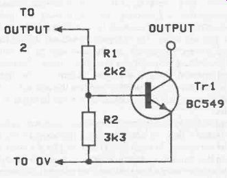
Fig. 15. Adding an open collector output stage to the light pen
Components for Light Pen (Fig. 14)
Resistors (all Vs watt 5%)
R1 3k3 R2 3k3 R3 1k
Potentiometer
VR1
Capacitors C1
Semiconductors
Tr1 Tr2 , IC1 D1 470k sub-min hor preset
100µ 10V elect BC549 BC557 74LS14 see text
Miscellaneous
Case, about 1 meter of fiber optic cable, wire, etc,
Construction of this project should offer little of real difficulty, and it should be possible to fit the electronics into virtually any small plastic case. Obviously the plug used to make the connections to the computer must be varied to suit the particular machine you are using. The computer's manual should have the necessary connection details, or there should be an advanced manual available which contains this information. The manual or advanced manual should also give details of the light pen registers, and there is little point in building the unit unless you are sure that you can find the information needed in order to utilize the device.
As explained, earlier, it may be necessary to resort to trial and error in order to find out which output is the correct one for your particular computer. In most cases there will be a +5 volt supply output on the computer which can be used to power the light pen (which consumes only a few milliamps of current). Remember to prepare the free end of the fiber optic cable so that so that the light from the screen is efficiently coupled through to the photo-diode.
It is by no means essential to fit some form of hand grip onto the free end of the cable, but as fiber optic cable is quite narrow it is advisable to do so as it can be awkward to hold for long periods of time. There should be no difficulty in fitting something like the case of an old ball-point onto to end of the cable.
The resolution provided by the pen is extremely good, and compares very favorably with the conventional light pens that I have encountered. Unfortunately, the supporting hardware in some computers is less than 100% reliable, and this can result in the occasional "glitch" with a totally wrong screen position being indicated. This can usually be effectively combatted in the software, with perhaps several readings being taken and averaged, with any that are well away from the average being deleted and a new average then being taken in order to determine the final answer. By this means it is usually possible to obtain accurate and consistent results.
With VR1 set at about half maximum value the light pen will probably work quite well, but it is worth experimenting with various settings to determine which one gives the best overall level of sensitivity and accurate results. One final point to bear in mind is that the pen detects light, and can therefore only read a screen position if the screen is reasonably bright at that position.