Grounding
Grounding is the cause of many problems in amateur-constructed equipment, but if thought about logically, there is no need for it to cause any problems whatsoever. Colloquially, the term ''grounding'' refers to the mains ground safety bond to the metal chassis, and also to the 0V signal wiring, but the two are quite distinct.
Ground safety bonding
The three wires leaving a domestic supply are line, neutral, and ground. Neutral and ground are connected together at the sub station or possibly at the electricity supply company's cable head within the house. This means that if line contacts ground, a fault current flows, determined by the ground loop resistance, which is the entire resistance around the loop, including the resistance of the line wires (see FIG. 25).
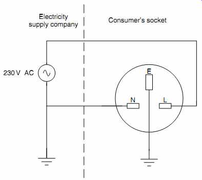
FIG. 25 How an grounded chassis and a fuse protect against shock.
The purpose of the ground safety bond is to provide a sufficiently low-resistance path to ground that if the line wire of the mains should come into contact with the exposed metalwork (which would then be a shock hazard), the resulting line to ground fault current is sufficiently great to rupture the fuse quickly. The time taken for the fuse to rupture is proportional to the ground loop resistance, so there is no such thing as an ground loop resistance that is too low.
Although exposed tubes may appear to conform to Class II, because the electrodes are insulated by a vacuum and the glass envelope, if the envelope is broken, the secondary layer of insulation also disappears. To ensure conformity, tubes on the top of the chassis should either be enclosed by a perforated metal cover to meet Class I, or insulating barriers to meet Class II.
If we build an amplifier on a chassis with exposed metal, then the construction must be to Class I and all hazardous voltages must be insulated from, and totally enclosed by, ground-bonded metal work. The ideal place to achieve this bonding is close to the entry of the power cable. The bond should be made using a solder tag bolted to the chassis with a shakeproof (star) washer between the washer and the chassis because this bites into the metal of the chassis and the tag to provide a gas-tight joint. If the chassis is anodized aluminum, the surface anodizing must be thoroughly scraped away underneath the tag to ensure a good bond.
The nut and bolt should be prevented from loosening using further shakeproof washers and/or locknuts. The ground bond bolt should never pass through plastic, such as the mains input socket, because plastic quickly creeps and causes the bond to loosen.
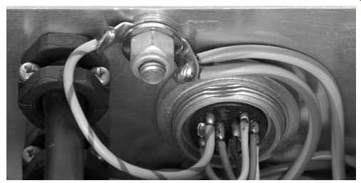
FIG. 26 A good ground bond maintains low contact resistance for the life
of the equipment.
The ideal ground bond would weld the incoming ground wire from the mains cable directly to the chassis, but this is not very practical. A perfectly reasonable alternative takes the incoming ground wire directly to an M6 or 0BA solder tag, where it should form a mechanical soldered joint. The tag is then screwed to the chassis with a shakeproof washer either side of the chassis, and another shakeproof washer above the ground tag, followed by a flat washer (to prevent the tag rotating when the bolt is tightened), then secured with a locknut. The nut and screw should be firmly tightened with a large screwdriver and a spanner after soldering otherwise the secure bond to the chassis prevents the iron from heating the tag (see FIG. 26).
A thick cable should be used to bring mains ground to the bond point in order to reduce ground resistance. Although it is permissible for 3A rated equipment to have 0.5 ohm of resistance from the pin of the mains plug to the chassis (not measured directly at the bond point), reducing this resistance to 0.1 ohm, or less, by using 2.5mm^2 mains cable, reduces the likelihood of hum and further improves safety.
The preceding arguments apply to equipment that is directly powered from the mains, but pre-amplifiers often have remote power supplies. Nevertheless, the same argument should still be applied, and a substantial cable should be used to transfer mains ground to the pre-amplifier chassis, and the bonding technique should be the same. Likewise, turntables should be firmly ground bonded via their mains cable, and not via a flimsy pick-up arm lead to a possibly indifferent mains ground.
Sometimes there will be metal that could come into contact with mains voltages but does not have a guaranteed electrical path to the mains ground bond. Examples of this are:
-- The acoustically suspended motor on a turntable.
-- A mains transformer or HT choke that is acoustically isolated because of vibration.
-- Any separate anodized aluminum panel supporting a mains connection, such as a front panel mains switch, or mains transformer on the baseplate.
Each of these should have a connection, such as a wire or a screw, via a star washer, to bond them to the main ground bond, but in the first two examples it is important that the wire should not be so stiff that it short circuits the acoustical isolation, so a loop or short helix of wire is ideal.
0V system grounding
It is the 0V signal ground connection to chassis that causes the hum due to hum loops between multiple grounds, not the safety bond.
Hum loops are circuits within ground paths that can have hum currents induced into them by mains transformers. Because there is resistance in the circuit, an unwanted voltage is developed, and this causes the audible hum (see FIG. 27).
To remove the hum, the loop must be broken, and this is often done by removing the ground wire from within the mains plug of one of the affected pieces of equipment, but this is extremely dangerous. The loop should be broken by removing the 0V signal ground bond to chassis from one of the pieces of equipment.
Fortunately, most modern equipment is double insulated, so hum loops do not often occur, but a modern improvement on Class 1 equipment is to provide a ground lift switch or plug gable link that can make, or break, the 0V signal ground to chassis connection at will on each piece of equipment. This method allows the optimum 0V system grounding arrangement to be determined quickly and safely.
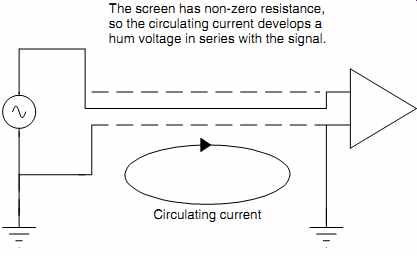
FIG. 27 How a hum loop causes audible hum---The screen has non-zero resistance,
so the circulating current develops a hum voltage in series with the signal.
--- Circulating current
Breaking the 0V signal ground to chassis bond Switches certainly start with low-resistance contacts, but the resistance rises as the contacts tarnish, especially if they are not cleaned by periodic use, as would be the case for a 0V signal ground bond switch, so a pluggable link is far better. The best pluggable link is the U-link used by telecommunications companies as the interface between their equipment and the customer's equipment in private telephone exchanges. The British U-link has a pair of linked 4mm plugs on 1/2" centers and provides a low-resistance path that does not deteriorate (see FIG. 28).
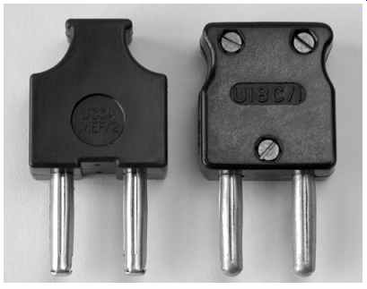
FIG. 28 A U-link intended for telecommunications use make an ideal removable
0 V signal ground to chassis bond
The U-link plugs into two 4mm chassis sockets, one insulated (connected to the 0V signal ground), and the other uninsulated and screwed firmly to the chassis with shakeproof washers.
Ideally positioning the 0V signal ground to chassis bond
We have seen that to avoid ground loops, there must be only one 0V signal ground bond to chassis, and hence mains ground. We should now consider the optimum position for this single bond.
An amplifier amplifies the difference between its two input terminals. We tend not to think of the 0V signal ground terminal as an input, but it is. In order to screen an amplifier, we surround it with a conductive casing/chassis connected to the amplifier's 0V signal ground. Inevitably, there is capacitance from the chassis to mains. Similarly, there is capacitance from 0V signal ground wiring to mains. Both capacitances return currents to the point where they are connected together. The further we are from the bond, the larger the unwanted voltage drop developed across the non-zero resistance.
A moving magnet RIAA stage having 2mV nominal sensitivity has a sensitivity of 284 mV at 50Hz, so it cannot tolerate any unwanted voltage drop. Thus, the optimum place to bond the 0V signal ground to chassis is at the input of the RIAA stage.
The bond should be made with as short and thick a wire as possible, in order to reduce its inductance and ensure that it is a good bond even at RF.
Interconnects, screens, and their grounds
The 0V signal ground is a signal wire because it allows the signal current to return to the source. It is therefore most important that we treat it with the same care and consideration that we would apply to the more obvious signal wires.
It is worth treating signal line and ground as though they are true balanced signals, even in an unbalanced system. The author has used twisted pair/overall screen interconnect cables on unbalanced systems since 1976 because of their superior rejection of external fields, but it is important that the screen is connected to 0V signal ground at the source end.
The screen should be grounded at the source end because the source has a low output impedance and can firmly define its output voltage as the difference between the two output wires.
One of these wires is connected to the screen of the output cable. The screen picks up RF interference which it super imposes onto the commoned signal wire. The RF is also super imposed onto the other signal wire via the output impedance of the source, and if the source has a truly zero output impedance at RF, both output wires now have the full RF superimposed on them. This might seem undesirable, but...
At the amplifier end, the input stage responds to the difference in signal between the two input wires, and therefore rejects the RF that is identical on both input wires.
If instead we connect the cable so that the screen is commoned to the grounded side of the signal at the destination end, the induced RF picked up by the screen now has to travel down the entire length of the cable to the source before it can be coupled via the output impedance of the source to an inner wire. Once coupled, the RF then has to travel the entire length of the cable before it can arrive at the amplifier input.
The RF signal on one wire has now had to travel twice the length of the cable, but has suffered the effects of series inductance and shunt capacitance which form a low-pass filter. This means that one of the wires at the input to the amplifier has the full RF signal, and the other has an attenuated signal, resulting in a difference signal to which the amplifier is sensitive.
The previous argument assumes equal impedances to RF ground (whatever that might be) at the pre-amplifier input. Whilst this is not necessarily true for domestic equipment, the quasi balanced method of interconnecting cables described is a considerable improvement on coaxial cable or ''screened lead'' because domestic impedances cause the two wires (the inner and screen) to have wildly different signals induced into them and there is no possibility of common mode rejection at the receiving amplifier.
Internal ground wiring of amplifiers
Once within an amplifier, the 0V signal ground path can either travel in the same way as it did between equipment, in which case, it is known as ground follows signal [1] or it can be star grounded.
Ground follows signal is the traditional method of wiring tube amplifiers, and is the easiest to do properly. The traditional method uses an ground bus bar which is a thick (at least 1.6mm diameter, or 16 swg) tinned copper wire 0V signal ground connected directly from input sockets to the 0V signal ground, or source, of the power supply (commonly the reservoir capacitor, or if fitted, the 0V output of the regulator).
The repetition of ''0V signal ground'' may seem pedantic, but it reminds us that the signal ground also carries power supply currents. This last factor is extremely important, since the power currents are often many times larger than their associated signal currents. Because individual stages amplify voltage differences referenced to their local ground, the ground bus bar needs low resistance to minimize the spurious voltages developed by power supply or signal currents passing through it.
Even the precaution of having a low-resistance bus bar is not sufficient, so connections must be made to the bus bar in the correct order such that voltages are not developed in sensitive input circuitry. The author remembers an RIAA disc pre amplifier that had been constructed to the Mullard 2- tube design, but had considerable hum. The hum was cured by moving one wire 150mm along the (1.6mm) ground bus bar.
The correct order from the input socket is input circuitry (such as shunt capacitors, etc.), grid leak resistor, cathode bypass capacitor (if fitted), cathode resistor, any anode signal circuitry (such as equalization), next tube's grid leak resistor, etc. If in doubt, think current rather than voltage. Decide whether you would be happy for a particular current to develop a voltage at a particular point along the bus bar and whether that voltage would then be amplified.
Depending on grounding arrangements, the ground bus bar may need to be firmly bonded to the chassis via a solder tag. Traditionally, one of the screws retaining the input tube socket was used as an ground bond, but all of the rules regarding mains safety grounds still apply, and a few milliohms of contact resistance is sufficient to cause an irritating hum, so a large screw that can be tightened down firmly with proper shake-proof washers is best. Centre spigots of the tube-holders (if fitted) should also be bonded to the bus bar as they help reduce capacitance between pins of the tube socket.
To make a neat ground bus bar, the thick wire needs to be straightened, and this is not a trivial task. The traditional way to achieve this is as follows:
Grip one end of the wire in a vice, and then grip the other end in a substantial pair of pliers, such as would be used for working on a car. The wire is than wrapped one turn round the jaws of the pliers, and the pliers are firmly gripped with both hands whilst one foot is braced against the vice. The wire is then firmly pulled until it can be felt to stretch, and without moving the position of the pliers is cut at the vice end. A beautifully straight piece of wire is now the result and this can now be cut away from the pliers.
It should be realised that considerable force is required to achieve this result, and this can apply dangerous forces to your back if you do not position yourself correctly. If you are in any doubt as to how to position yourself, or have back problems, do not attempt to use this method. It is far better to have tatty wiring that can be seen, than beautiful wiring that cannot be seen because you are lying down with your back in traction.
Unfortunately, tinned copper wire oxidizes over time, and becomes difficult if not impossible to solder, but a beautifully shiny and easily soldered surface can be restored by a quick polish using metal polish intended for brass. A wipe with isopropyl alcohol or methylated spirits will remove the last traces of polish and enable perfect soldered joints.
The ultimate expression of the ground bus bar is the RF ground plane, which is a two-dimensional conducting grounded surface to which ground connections are made (a wire is only one-dimensional).
This construction is now common on audio printed circuit boards as designers have realised how important RF immunity is to audio circuitry. On a PCB, the entire upper surface of the board can be used as an ground plane, which has low inductance because it is so wide, and therefore guarantees a good RF ground at every point that a contact is made.
An alternative hard-wired approach is to use a strip of 10mm x 1mm silver or copper as the bus bar. The very large cross-sectional area ensures low resistance, whilst the width lowers the inductance and makes soldering fractionally easier.
Holes can be drilled into the bus bar to suit component wire diameter, or V notches filed at the edge to locate the component whilst soldering. The iron should be held to the strip first to bring it up to temperature, then moved so that it touches the component, and more solder applied to form the joint. A 200W iron is needed, as a smaller iron takes so long to warm the bus bar to soldering temperature that it damages adjacent components.
Some classic tube amplifiers (such as the Rogers Cadet III) approximated to a ground plane by soldering to conductive posts pressed directly into the (steel) chassis, and using this as the 0V signal ground. Neither this method nor a steel chassis is recommended for a new design.
Star grounding is achieved by having a single ground point, perhaps bonded directly to chassis, to which all 0V connections are brought individually. Ideally, all the connections to this point are made with short leads to minimize inductance and noise, but building an entire amplifier using this method can become a little fiddly (see FIG. 29).
Because of the difficulty of making so many 0V connections to a single tag, many constructions use a combination of star and bus bar grounding, with the input stage star grounded, and following stages grounded to the bus bar.
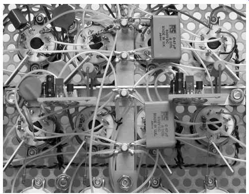
FIG. 29 True star wiring uses many wires, but is manageable with care.
Stars from top to bottom; 0 V signal ground, +270 V, +160 V, -335 V
Rectifiers and high-current circuitry
Although low-voltage bridge rectifiers are commonly available, they typically use standard diodes rather than Schottky or soft recovery, so we often need to make our own bridge rectifier and if we choose diodes that are in an insulated package (such as STTA512F, rather than STTA512D) fitting them to an aluminum angle bracket (to allow heatsinking) is easy (see FIG. 30).
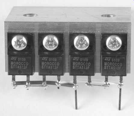
FIG. 30 Insulated diodes make bridge rectifier construction easy
Some parts of an amplifier unavoidably carry high currents.
In a capacitor input power supply, the loop from the mains transformer via the rectifier to the reservoir capacitor carries the capacitor ripple current, so it is essential that no connections are made to the 0V signal ground within this loop because the large current would develop a noise voltage across the unavoidable wiring resistance. The two circuits are split at the reservoir capacitor. Assuming that the reservoir capacitor has screw terminals, it is best to connect the solder tag directly contacting the capacitor to go to the rectifier/transformer and the one further from it to go to the load (This means that the high currents in the capacitor/rectifier/transformer loop cannot develop a voltage in the load circuitry.) (see FIG. 31).
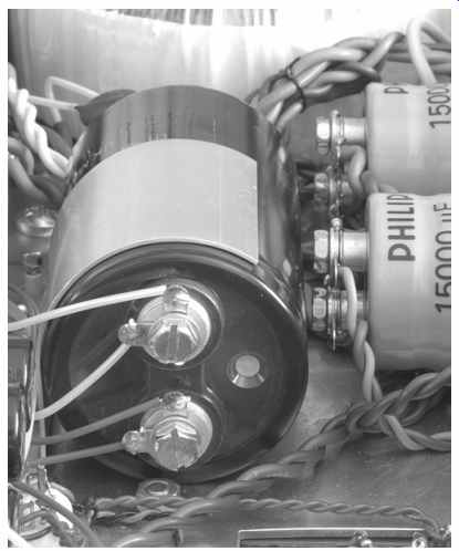
FIG. 31 Star connections to a reservoir capacitor reduces interaction
between incoming and outgoing currents.
In order to minimize the electromagnetic field caused by the passage of transformer to reservoir capacitor currents, this loop should ideally be made of twisted pair to minimize its area, and be as short and thick as possible to reduce its resistance and voltage drop.
A power amplifier's output stage is effectively supplied from a single capacitor, so output tube cathodes should be brought individually to the 0V terminal to form a star. Similarly, individual wires from output transformers should be brought individually to the HT terminal to form a star (see FIG. 32).
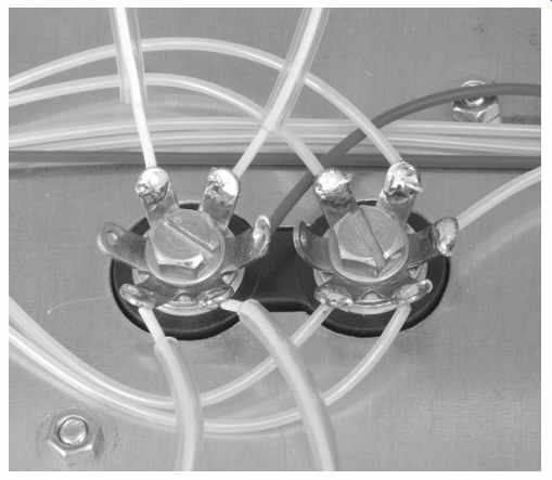
FIG. 32 Star connections to the capacitor feeding the output stage minimize
inter actions between tubes.
The output to the loudspeaker from a power amplifier is also a high-current loop, and additional connections to sense this voltage, such as global negative feedback, should be made very carefully. The ideal method is to connect a screened twisted pair to the output terminals, with the screen connected to chassis at one end only (to prevent loop currents flowing in the 0V signal ground). This cable is then routed to the input stage, where one side is connected to the lower end of the cathode resistor, and the other is connected via a series resistor to the cathode (assuming cathode feedback). This method ensures that the feedback voltage is derived from the correct point and presented to the correct point (see FIG. 33).
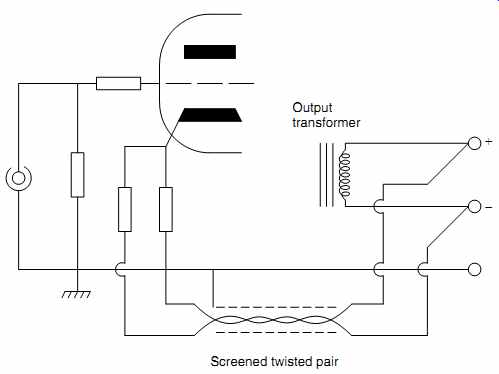
FIG. 33 Screened twisted pair derives the feedback from the correct point
(amplifier output terminals) and prevents induction from transformers entering
the feed back loop, then applies the feedback at the correct point.
Layout of components
There are various approaches for positioning the smaller components such as resistors and capacitors, ranging from one extreme to the other:
1. Position the components in a regimented manner in neat lines and use neatly harnessed wiring to make the complex interconnections. The parallel wires in the harness inevitably increase stray capacitances, but this method was used in the Quad II power amplifier (see FIG. 34).
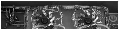
FIG. 34 The Quad II harnessed its wiring into a loom, increasing capacitance
2. Position the components in a regimented manner in neat lines, and either use hidden wiring which can be untidy (Leak), or exposed neat wiring (Mullard recommendations) to make the interconnections between components. This technique reduces capacitances compared to method (1), but can take up significant space (see Figures 35 and 36).
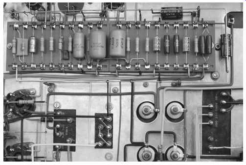
FIG. 35 This fine example of a Mullard 5-20 was spotted at a radio fair.
Ideally, the 0 V signal ground bus bar would contact the chassis at a single
point, rather than at each support.
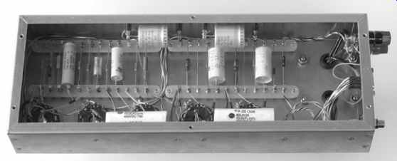
FIG. 36 This 10W amplifier is one of a pair used in an ''old technology''
TV monitor project and receives power from the central power unit rather than
having its own supply.
3. Methods (1) and (2) had regimented rows of components enforced upon them by the layout of the tags on the boards.
If that restriction is waived, then a small resistor no longer takes up the same amount of space as a large coupling capacitor and space is saved. The hidden wiring becomes copper tracks and the board becomes a printed circuit board (PCB).
4. The preceding methods are two-dimensional. Interconnecting wire length can be further reduced if the assembly becomes three-dimensional. Components are now soldered directly to tube sockets and if necessary, to nearby stand offs, or perhaps a tagstrip. This is potentially the best construction method, but it needs careful thought to keep the components even reasonably tidy and accessible for testing/ maintenance. Tagboards, tagstrips, and stand-offs are all useful ways of supporting components and joints insulated from ground (see FIG. 37).
At tube impedances, practical inductances are completely insignificant except in the 0V bus bar, so good layout in a tube amplifier requires low stray capacitances, and the best way of reducing capacitance between wires or components is to cross them at right angles. Capacitance to ground is minimized by short leads. One approach that is not immediately obvious is that sleeved wires have higher stray capacitance than self-supporting bare wires because Εr >~1. It is the combination of these requirements that forces component layouts that appear to have been thrown together by an avant-garde sculptor. We thus arrive at the surprising conclusion that a good component layout probably looks untidy, but the converse is unlikely to be true (see FIG. 38).
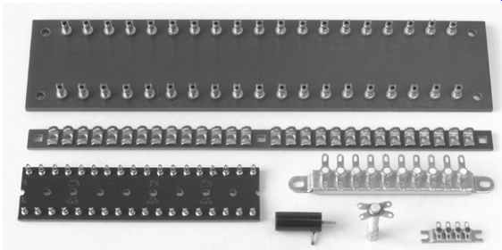
FIG. 37 A selection of tagstrips, tagboards, and stand-offs
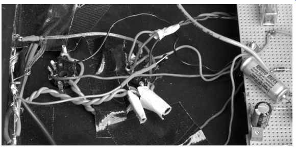
FIG. 38
Bad practice: How many howlers can you spot?
This appalling example features a variety of bad practices:
-- Gaffer tape: Gaffer tape is for bodging on stages and studio floors, not internal electronic use.
-- Terrible soldering: As a single example, the thickest wire on the ground bus bar was clearly soldered by an iron having an insufficiently large tip, resulting in poor solder flow and damaged insulation.
-- Ground bus bar: The ground bus bar should carry the 0V signal ground from the tube to the input socket, not the screened lead. Thus, the bus bar is heading in the wrong direction -- it should pass over the tube sockets.
-- Screws: The screws securing the tube sockets are too long.
It's very difficult to install good heater wiring when your fingers keep hitting obstacles.
-- Heater wiring: The wire is too thick and stranded, and because the wire wasn't pre-tensioned before twisting, these factors resulted in a loose twist just where a tight twist is most important (near small-signal tubes).
-- Diagonal components on matrix board: Diagonal components do not themselves cause problems, but they do indicate a poorly planned layout.
Whether the layout is a ''tidy'' PCB or an optimized hardwired layout, good layout requires considerable care, and thermal considerations must also be accommodated.
Making PCBs
Printed circuit boards have been mentioned several times, and the author uses them frequently, but they are not ideal for the novice. This is because they are really a production method of construction, and it requires considerable confidence to design a theoretical circuit and commit it directly to a PCB. Whilst it cannot be argued that a good PCB gives a thoroughly professional appearance to the finished project, hardwiring will often give superior performance. Despite these caveats, making a single-sided PCB is not nearly as difficult as you might think, and it doesn't need specialist equipment.
PCB layout
The hardest part is working out the layout. Unfortunately, achieving a good layout is very much like learning to ride a bicycle - easily done once you have experience, but tricky to describe to a novice.
Nevertheless, points to remember are:
-- If the circuit diagram was drawn well (connections in the right order), a good PCB will be laid out very much like the diagram.
-- Most components (except tube sockets) fit a 0.1” grid.
-- You are working from underneath (the foil side), so if you use ICs, remember to work out their pin-out as viewed from underneath. (IC manufacturers' diagrams give the pin-out view from above, whereas tube manufacturers give the view from underneath.)
-- A simple audio PCB should not require any links. If you need links, you probably haven't tried hard enough. (Or you used an autorouter in a PCB design program.)
-- PCB foil is thin, so it is vital to think about currents and ensure that you don't pass heavy currents through sensitive areas. Remember that you can always widen the track, or star tracks to a central point to minimize interaction between currents (see FIG. 39).
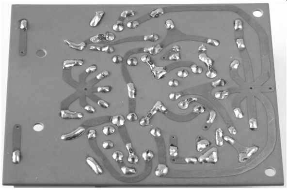
FIG. 39 Star ground and power on a PCB
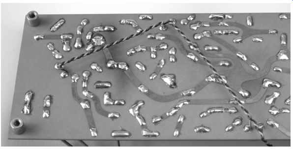
FIG. 40 Heater wiring on a PCB is best achieved with twisted pair
-- PCBs inhibit cooling, so try to put hot resistors or transistors near the edge where they can be bolted to a heatsink or can cool naturally. If you can't do that, raise them well clear of the board and give them space from other components to allow cooling air to flow round them.
-- Don't put power tubes on a PCB -- it's just asking for thermal problems.
-- If you put tubes on a PCB, don't even attempt to do heater wiring using PCB tracks, it makes layout of the audio almost impossible, and heater wiring is far better done afterwards with twisted pair spaced away from the board so that it rests snugly against the chassis (see FIG. 40).
-- Surface mount resistors make excellent grid-stoppers, and really aren't that difficult to use, but in order that surface tension aids positioning, rather than hindering, it's import ant that your PCB tracks are the same width as the component. You need the smallest tip on your iron and _0.5mm silver-loaded solder. Tin the tips of the two tracks with the absolute minimum of solder, position the resistor with tweezers, and with a slightly wetted iron, reflow the solder at one end to form a badly soldered joint. Solder the other end properly with a little fresh solder, then return to the first joint and solder it properly with a little fresh solder. It's actually more difficult to describe the process than to do it!
-- Pre-amplifiers tend to need a lot of connections to ground, so a double-sided PCB with the component side used as an ground plane not only helps layout, but improves screening. If you use an ground plane, radial-leaded capacitors such as Wima FKP1 obscure their leads on the component side, so you need to bend their leads horizontally (without stressing the component) and solder directly to the ground plane. They don't, therefore, need a hole to be drilled through the board for this connection.
-- A power amplifier's driver stage usually has its tubes showing on the top of the chassis, but PCB capacitors can sometimes be quite tall, forcing the PCB to be mounted so far below the chassis that the tube hardly peeps through the chassis, restricting cooling. In this instance, it is better to mount the tube sockets on the foil side (beware that from the point of view of the tracks, this reverses the pin order).
Unfortunately, mounting the socket on the foil side is mechanically weak because removal of a tube tends to tear tracks off the PCB. The solution is to choose a flanged PCB socket and use PCB mounting spacers of just the right length to press the flange against the chassis plate (see FIG. 41).
-- If you are forced to have two tracks adjacent to one another that are hostile to each other (perhaps the input and output of an amplifier), you can always put an grounded track in between to guard them.
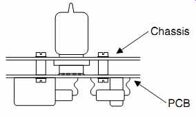
FIG. 41 The chassis can help in supporting tube sockets soldered to the
foil side of a PCB
There are two ways of working out the layout:
Method 1: You buy a pad of graph paper marked in 0.1" squares. This is usually described as ''10ths, 1/2 & 1 inch''. You then sit down with a 2H pencil and a plastic eraser and work out your layout. After much rubbing out and redrawing, you obtain an efficient layout, which you then copy onto a virgin sheet of graph paper.
Method 2: You use a familiar computer drawing program with ''snap'' set to 0.1"
-- After much shuffling and redrawing, you end up with an efficient layout and you struggle to make your printer print it the correct size. This process initially takes longer than Method 1, but it allows changes and copies later on.
Transferring the layout to the PCB
Either way, you now have a drawing the same size as your final PCB. Next, you cut the PCB material to size and clean the edges. Whether you use glass reinforced plastic (GRP) commonly known as FR4 (fire resistant type 4), or synthetic resin bonded paper (SRBP), the best way of tidying the board edges is to rub them down with 160 emery cloth held on a sanding block (for some reason, traditional cork sanding blocks are now expensive, but a scrap of MDF is fine). For a perfect finish, the edges can be smoothed with 300 grade silicon carbide paper. The inevitable burrs are best removed with the flat side of a half-round needle file (half-round needle files tend to be finer than flat ones).
Some constructors, having used a computer to produce their layout, print the layout onto a transparency. Ensure that the transparencies you use in a laser printer are suitable for photo copiers and/or laser printers, otherwise you will wreck your printer! You then buy some fresh PCB material coated with UV sensitive etch resist, put the PCB and transparency into a UV light box and take a contact photograph of the layout which is later developed. Note that the drawing must be ''mirrored'' before printing so that the printed side is in contact with the board. If the printed side is not in contact with the board, the image on the board becomes de-focused, leading to a poor PCB. Because this is a photographic process, exposure time is important, as is the density of the black that your printer can produce on the transparency. Additionally, film deteriorates with time, which is why you need fresh PCB material.
Alternatively, you could buy UV etch resist and spray the board yourself. If you buy the etch resist, carefully check the ''use by'' date and reject it if there is less than a year remaining. Treat etch resist, developer, and unused (coated) board like 35mm film, and store them in a fridge to maximize their shelf life.
Correctly made photographically produced PCBs have a perfect finished appearance, but severely restrict your choice of PCB material unless you are prepared to coat boards yourself. Additionally, UV light boxes are not cheap, and practice is required to achieve correct exposure. Because of these photographic problems, the author still uses a very low technology method.
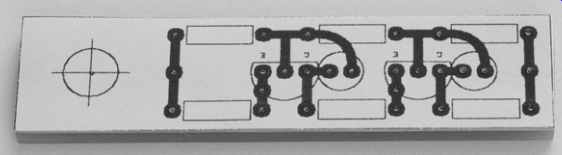
FIG. 42 Marking ''join the dots'' holes through the paper template
Cut the board of your choice to size and wash/scrub the foil with a soap-filled scouring pad until the copper gleams. Stick the paper layout gently to the foil side. Use a scriber to mark all the component and fixing holes through the paper (see FIG. 42).
Carefully remove the paper. Wash the board again under very hot water so that no trace of glue remains. Wash your hands thoroughly. Dry the board, and handle it by the edges only.
You now have a board covered in dots. Sit down at a well-lit table, put some Bach on (greatly helps concentration), take a 00 sable paint brush, a pot of well-shaken enamel paint, and ''join the dots''. It is not necessary to be a painter of the caliber of Michelangelo, just to have a steady enough hand to paint smooth curves that do not touch. Preparing the board for painting tenses the muscles, and you will find that you produce better work if the board is prepared the day before, so that you have a relaxed, steady hand. It is most important not to touch the foil, as grease/sweat could impede the sub sequent etching process, so an artist's Mahl stick to support your wrist can be very useful when painting large boards (see FIG. 43).
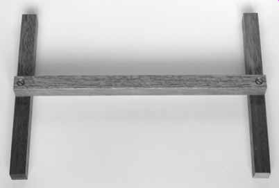
FIG. 43 This easily-made Mahl stick prevents accidental contact with the
PCB
The author uses red paint because it is easy to see errors against the copper backing (see FIG. 44).
If you are impatient, once painted, you will arrange for a gentle draught of warm air over the board to dry the paint quickly.
Whilst this is happening, wash your brush carefully in white spirit followed by warm soapy water.
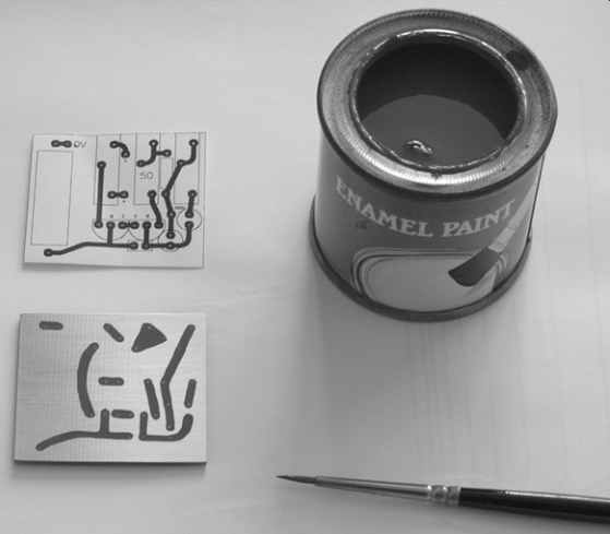
FIG. 44 The PCB is painted and ready for etching
Etching
Printed circuit boards are etched using ferric chloride solution. Ferric chloride granules are available from all electronics factors-just add water. Bear in mind that it is intended for etching, so it is highly corrosive, and should be stored in a PVC container. Fruit juice bottles are a possibility, but label the container conspicuously and keep it away from inquiring hands.
Assuming that you have a board covered with developed etch resist or dry paint, it is time for etching. Warm etching fluid works far faster than cold (chemical reactions double in speed with each 10 degr. C rise in temperature). The author fills his PVC etching tray (an old lunch box) to a depth of 1/4" (_6mm) and discretely pops it in the microwave for a couple of minutes to warm it gently before etching. Have plenty of kitchen roll handy at all times in case you accidentally spill a drop.
Ease the board gently into the etching fluid foil side up, and rock the tray gently and continuously to clear etched debris from the surface of the board. After a few minutes you will see the board begin to etch around the edges. Continue agitating the fluid and watching. Depending on temperature, foil thickness, and age of fluid, the process takes between ten and twenty minutes.
It is most important not to leave the board in the etchant for too long or it will undercut the tracks beneath the resist. When etching appears to be just complete, give the board another minute to be certain. Place your bottle of etching fluid in the sink, turn the cold tap on, and pour the fluid back from the tray into the bottle. If you should spill any etchant, it will immediately be diluted by the running water and the sink will not be stained. Put the bottle of etchant away, and run water gently into the etching tray to dilute the remaining etchant and allow it to overflow until clean water results. You can now retrieve the board (see FIG. 45).
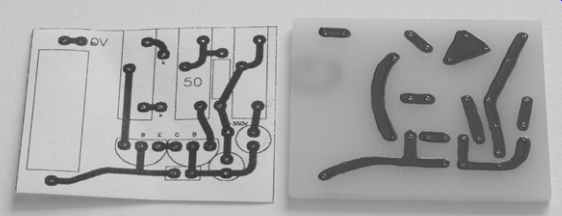
FIG. 45 PCB etched.
The etch resist can now be removed. If you painted the board, pour chemical paint stripper generously onto the board, wait a minute or two, and wash it (and the paint) off with an old toothbrush under running cold water. Don't press hard with the brush or you will scrub paint into the board never to be removed. By now, your hands are probably becoming greasy again, so wash them thoroughly. The board is now ready to be drilled (see FIG. 46).
Drilling
If you use FR4, you need silicon carbide drills. Ordinary high speed steel (HSS) drills do work, but they blunt quickly.
Typical hole size is 0.8mm, but you may wish to measure components individually and drill holes precisely sized for each component to ensure the best possible solder joint. Small drills must be treated carefully and ideally need very high drilling speeds. A drill in a stand is essential. Provided that the stand is well greased and adjusted, even a power drill can be used to drill <1mm holes, but it will probably need a pin chuck to hold the drills (see FIG. 47).
Stuffing and soldering
Once drilled, the board can be stuffed. Component leads should be cropped short before soldering, otherwise the mechanical shock from cropping disturbs the soldered joint (see FIG. 48).
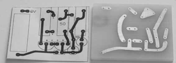
FIG. 46 PCB stripped
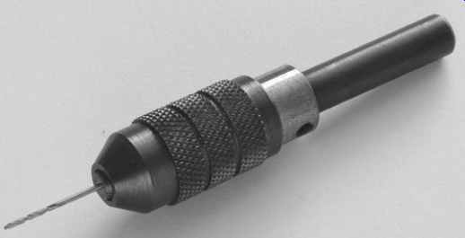
FIG. 47 A pin chuck allows very small drills (<1:5mm) to be used FIG. 48 The board has been stuffed, leads cropped, and is ready for soldering
Once soldered, it is well worth removing the flux from a PCB.
The act of soldering causes a small explosion as the flux heats, causing droplets of solder and flux to be sprayed over the surrounding area. On a PCB, this can cause electrical leakage, so although flux removing fluid is messy stuff, it ensures correct operation of the completed board (see FIG. 49).
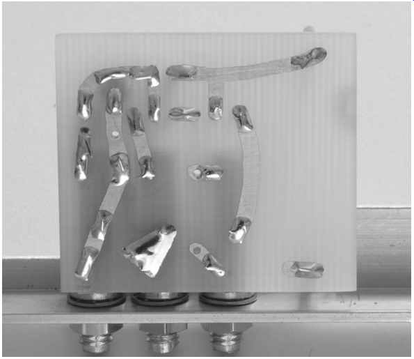
FIG. 49 The joints have been soldered and de-fluxed.
Although a board is a sub-assembly, there is no reason why it should not form part of a larger sub-assembly. In this particular case, each board is a constant current sink that ultimately controls the total anode current and balance of a pair of output tubes in a push-pull stereo power amplifier (see FIG. 50).
The aluminum bracket supports a pair of PCBs by their trimmer potentiometers, which have been positioned so that their shafts align with the holes in the perforated aluminum sheet to which this bias assembly will be fitted.
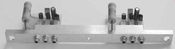
FIG. 50 A pair of boards on a bracket form a larger bias sub-assembly.
Modifying PCBs
Although it might seem that a circuit constructed on a PCB is set in stone, modification is perfectly possible -- it just takes care.
Phenolic boards are far more fragile than glass-reinforced plastic boards (FR4, etc.), so decide carefully how you will remove a component before attacking the board.
Never attempt to salvage components. If you bent the wire over before soldering, the component will not come out simply by heating the solder and pulling from the component side. Cut the component away from the component side and use a sharp point such as a needle or a dedicated PCB rework tool to push each lead through whilst heating the solder on the track side. Once a wire fragment stands proud, it can easily be removed by a pair of fine nose pliers or tweezers.
Never tug on wire fragments -- you could tear a track away from the board. Sometimes it helps to remove some of the solder from the track side before removing a wire fragment.
Paradoxically, you don't want to remove all the solder because this makes it difficult to get the heat into the remaining solder that bonds the unwanted component to the track. Desolder braid is a safer option than a desolder gun -- the recoil can kick tracks away.
The replacement component may not be the same length as the original. Don't attempt to force the wires on the new component to fit the old holes, use one old hole and drill a new hole to suit (make sure that you don't accidentally drill into another track!) Pass the wires through, bend the wire from the blank hole so that it contacts the track you want, and solder it.
Sometimes you need to cut and remove a section of track. A sharp scalpel easily cuts the thin copper foil, so you don't need to murder the board. Make a cut either side of the section of track to be removed, tin the track, heat it with the iron, and use the tip of the scalpel to ease the unwanted track away. If you are careful, it is possible to remove sections of track without anyone knowing you've been there.
Sometimes you need to add a track from one side of the board to the other. The standard industry technique is to use green (any color would do, but green is used) wirewrap wire to make the link. Cut the wire to length, and strip 1/2" from each end. Tin each end to allow the stress of stripping to be relieved and shrink back the insulation, and trim the exposed wire to 1-2mm as appropriate for the job, then solder. If the wire is long, a few small spots of glue can be used to secure it.
If you need to add some circuitry and there's a blank piece of board, it's surprising how neat a job can be achieved by drilling holes for the components and bending and soldering their wires together on the track side in lieu of tracks.
Hardwiring modules
A high-voltage bridge rectifier with each arm composed of three diodes and snubber capacitors can be rather bulky if hardwired on tagstrip or terminal board, and making it on a PCB is inviting tracking. A method that can be useful is to glue the capacitors together using a hot melt glue gun, then fit the diodes in appropriate positions. It can be quite tricky to deter mine how to position the diodes to minimize the wiring, but starting from the circuit diagram of the rectifier and gradually metamorphosing it to the required shape helps (see FIG. 51).
Once the layout has been decided, the compact rectifier can be neatly constructed, then potted (see FIG. 52).
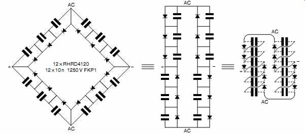
FIG. 51 A compact mechanical layout for an HT bridge rectifier can be
gradually developed from the circuit diagram FIG. 52 Once laid out, the
rectifier can be constructed quickly and neatly, then potted
Exercises and solutions
The following section covers techniques that you may find useful but that don't sit neatly in previous sections.
Identifying the outer foil of a capacitor
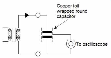
FIG. 53 Identifying the outer foil of a capacitor
Electrostatic noise pick-up is proportional to the capacitance between the noise source and the affected part, so large objects like coupling capacitors are especially vulnerable. Because capacitors are invariably wound as a coil of foil, the outer foil screens the inner foil, and should ideally be connected to ground.
Obviously, a capacitor coupling two stages together has neither end connected to ground, but the output of the preceding stage is a far closer approximation to ground than the grid of the next stage. Thus, coupling capacitors should have their outer foil connected to the output of the previous stage to minimize noise pick-up.
Unfortunately, the outer foil is not often marked, but it can usually be identified (see FIG. 53).
The capacitor under test is connected as a reservoir capacitor to crudely rectified AC, and a strip of metal foil is wrapped around the capacitor. The metal foil is connected to the input of an oscilloscope or an amplifier. If the outer foil of the reservoir capacitor is connected to ground, very little noise will be picked up, but if it is connected to the ungrounded output of the rectifier, the capacitance between it and the added foil will easily couple the higher harmonics of the rectified AC into the amplifier or oscilloscope. Thus, the outer foil can be identified by finding which connection creates the most noise. Unfortunately, this method doesn't work for polypropylene capacitors because they are often made from two capacitors in series placed end to end, so they don't strictly have outer and inner foils.
High-current (>2A) heater regulators that shut-down at switch-on
Single-ended amplifiers cannot cancel heater-induced hum from directly heated tubes in their output transformer, so one solution is to power the heater from regulated DC. The 5A LM338 is the ideal three-terminal regulator for the job, but its comprehensive protection can sometimes be tripped by the (much lower) cold resistance of a tube heater. If this occurs, the solution is to add a resistor between input and output of the regulator to bleed current directly into the heater. At switch on, the regulator shuts down, but the bleed resistor passes sufficient current to warm the heater, raising its resistance, eventually allowing the regulator to come out of shut-down.
The value of the bleed resistor is not critical, and setting it to pass 10% of the final current generally solves the problem.
Thus, if we had a 10V 3.25A heater and dropped 3V across the LM338 under load:
R = V / [0.1 x I ] = 3V / [ 0.1 x 3:25A] = 9.23-ohm = 10-ohm
Under working conditions, the 10-ohm resistor will only dissipate 0.9W, but at switch-on, it must pass a much higher current, so an aluminum-clad resistor bolted directly to the chassis is ideal.
Tarnished silver-plated stand-offs that won't solder Silver tarnishes when exposed to air, so 30-year old silver plated stand-offs are unlikely to be solderable. However, dip ping the tag into Goddard's Silver Dip converts the tarnish back to silver, enabling soldering. As with all chemicals, Silver Dip should be handled with care, and only the silver-plated tag of the stand-off should be allowed to touch the liquid, but mounting them on a scrap of cardboard neatly solves this problem (see FIG. 54).
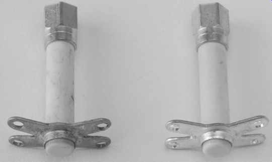
FIG. 54 Silver-plated tags before and after dipping in ''Silver Dip''.
Rinse the stand-offs in clean water, and dry them with forced hot air from a hair dryer. Although this technique is very effective, it is rather smelly and the tags tend to tarnish soon afterwards, so it is best to treat the stand-offs just prior to use.
NOS tube sockets that won't solder
NOS tube sockets are likely to be at least 25 years old, and the (usually tinned) tags will be reluctant to solder -- this seems to be a particular problem with Loctal and Septar PTFE sockets.
Taking a wire brush to the pins is not a good idea because even a fine wire brush scratches the insulation supporting the tags and embeds those scratches with particles of (conductive) solder, making the base much leakier. One solution is to soak them in a jar of isopropyl alcohol for a day or two, periodically giving the jar a good shake. Really recalcitrant sockets can be periodically removed and brushed with a toothbrush until the tags become clean and shiny. Finish with a good rinse in clean alcohol, followed by clean water, and dry them with forced hot air from a hair dryer.
The alcohol quickly becomes dirty, but can easily be recovered by filtering it through a coffee filter paper supported in a stainless steel kitchen funnel (the alcohol could damage a typical plastic funnel). Be aware at all times that isopropyl alcohol is highly inflammable, so don't smoke whilst handling the stuff!
Enlarging the hole for the wire in a solder tag
You might think this is easy, but solder tags are made of brass, and brass has a nasty habit of snatching when you drill it.
Given that tags are small, you've only just discovered the problem, and you want to get on with wiring, this is the perfect recipe for slicing the tip of your fingers. The solution is a small taper reamer (see FIG. 55).
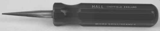
FIG. 55 Tapered reamer for enlarging small holes.
This is a very handy tool to keep with your wiring tools.
Because it cuts a tapered hole, it needs to be used from both sides of the hole. It throws up a burr, but this isn't a problem, because when you fold your wires around the joint to form a mechanical joint before soldering, the high pressure at the burr makes an excellent contact even before you solder.
Reference
1. ''Designing a professional missing console: Part Six -- When is a Ground not a Ground?'' Steve Dove, Studio Sound. March 1981. pp 56-60.