By Forrest M. Minns
IN THIS day of ultra-sophisticated semiconductor technology, large-scale and very-large-scale integrated circuits (LSI and VLSI respectively) containing hundreds or even thousands of logic gates have become commonplace. Nevertheless, examine any board containing one or more LSI or VLSI chips and you'll probably find an assortment of small- and medium-scale integrated circuits (SSI and MSI) with relatively few gates or flip-flops package.
Circuit designers have long wanted to combine in a few packages the relatively small number of gates and flip-flops required to support most LSI and VLSI chips. Custom ICs are usually out of the question because of their high price and long development time. And what happens if a design change is necessary? Semi-custom integrated circuits are a better choice. These chips contain arrays of gates which have not been metalized. In other words, the gates are independent of one another since they've not yet been connected together electrically by a metallization pattern on the top surface of the chip. The customer tells the custom IC house how he wants the gates interconnected, and the gate chips are then metalized according to the customer's specifications and installed in DIPs.
This procedure is faster and cheaper than the custom IC route, but it's still relatively expensive since the customer usually must agree to buy a thousand or more chips. And as in the case of the custom IC, what happens if a design change is necessary? A third alternative is the do-it-yourself logic chip. Included in this category are field programmable logic array (FPLA) and programmable array logic (PAL, a trademark of Monolithic Memories, Inc.) chips. These chips contain arrays of logic gates interconnected via the same kind of fusible links used to make programmable read-only memories (PROMs). By selectively applying high-current pulses to the programming pins of an FPLA or PAL, fusible links can be opened in various patterns to produce a customized integrated circuit.
The PROM is itself a versatile do-it-yourself logic chip since it can be used to implement any truth table for which it has sufficient inputs and outputs.
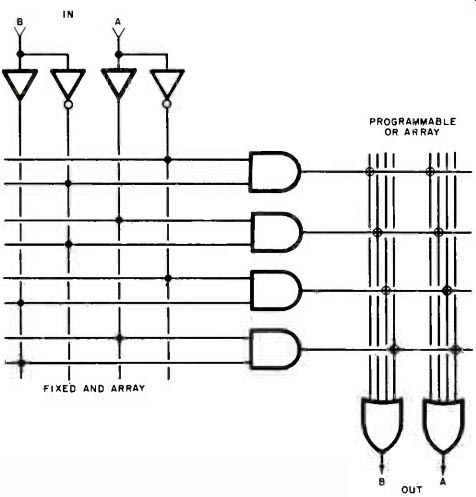
Fig. 1. A PROM of four two-bit words The AND array is fixed; the OR
is programmable.
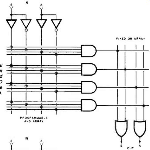
Fig. 2. A hypothetical PAL of two four-bit words. it is a backward
PROM since the AND array is programmable while the OR is fixed.
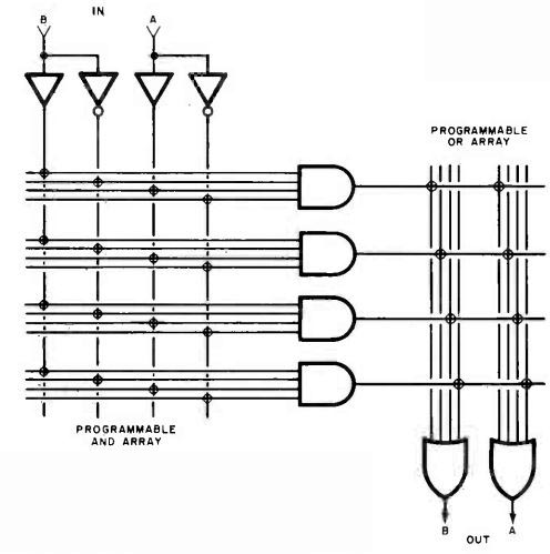
Fig. 3. An FPLA of two four-bit words. Both the AND, and the OR are programmable.
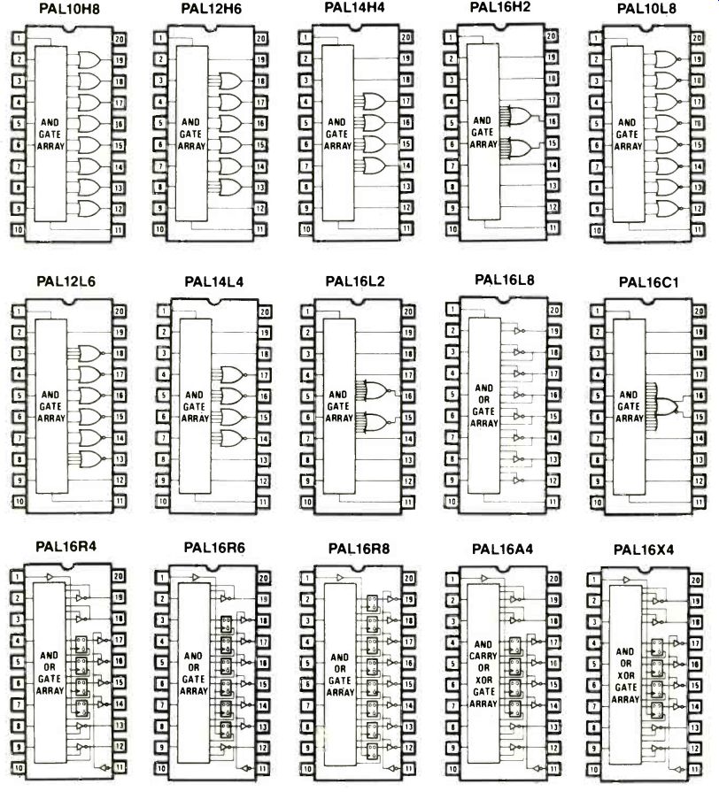
Fig. 4. Pin outlines and internal block diagrams of the PAL family
of chips.
You can better understand the operation and compare the differences of PROMs, FPLAs and PALs be referring to Figs. 1, 2 and 3. They show the internal circuitry of ultra-simple, hypothetical versions of each of these three kinds of programmable logic arrays.
As is readily apparent from these figures, all three circuits contain an AND array followed by an OR array. The input word applied to the AND array can be considered an address, data word or bit pattern. In any case, the effect is the same since a particular input switches the output of one of the AND gates from low to high. The outputs then reflect whether or not connections are present at the junction of the output line from a selected AND gate and the input lines to the OR gates.
A solid dot at the intersection of two array lines means the connection was unalterably programmed when the chip was made. User programmable fusible links are indicated by small circles at intersection array lines.
In the PROM (Fig. 1), the AND array is permanently programmed or fixed while the OR array is programmable. The AND array in Fig. 1 is programmed to address in turn each of the AND gates from top to bottom according to a standard 00, 01, 10, 11 input sequence.
The PAL (Fig. 2) is a backward PROM since the AND array is programmable while the OR array is fixed.
In real PALs the OR array is factory programmed to give some of the most commonly used logic functions.
The FPLA (Fig. 3) is the ultimate do-it-yourself logic chip since both the AND, and OR arrays are programmable. While this provides the highest degree of flexibility, in practice the FPLA is much more difficult to use and more expensive than either the PROM or the PAL. All three kinds of chips can be programmed using standard PROM programmers, but the programming procedure for the FPLA is at least twice as cumbersome since both the AND, and OR arrays must be programmed.
Some PALs and FPLAs include flipflops to store output states and feed results back to the inputs. This makes possible such functions as counting, shifting and sequencing.
PALs without flip-flops can perform virtually any task now accomplished with SSI and MSI logic chips up to and including a 4-bit arithmetic logic unit! In many applications a single PAL can replace up to ten SSI/MSI packages.
A clever feature of PAL chips is a data security fuse. After the PAL has been programmed, the security fuse is blown to disable the circuit's internal verification logic. This prevents the internal program from being read out by a potential copier, thereby making the chip proprietary.
The PAL concept was pioneered by John Birkner of Monolithic Memories, Inc., and that firm now makes a family of fifteen PAL chips with National Semiconductor as a second source. Figure 4 shows the pin outlines and internal block diagrams for all fifteen chips. As you cap see, considerable flexibility is provided by this lineup.
Information about PALs and FPLAs is not too abundant. The best way to learn more about PALs is to contact a Monolithic Memories or National distributor or representative. Try to obtain a copy of the excellent "PAL Programmable Array Logic Handbook" published by Monolithic Memories (1165 E. Arques, Sunnyvale, CA 94086). Signetics ( P.O. Box 9052, Sunnyvale, CA 94086) is a major maker of FPLAs.
Their "Bipolar and MOS Memory Data Manual contains FPLA data sheets and related information. Two Signetics engineers, Napoleone Cavlan and Stephen J. Durham, have written an excellent two-part article of the subject for Electronics (July 5, 1979, pp. 109-114 and July 19, 1979, pp. 132-139). In an article for Computer Design (April 1980, pp. 141-147), Mr. Durham described a complete 60-character keyboard encoder complete with key de-bouncing and made from a single Signe-tics 825105 FPLA! You can find the aforementioned articles in any good public or university library. For manufacturer's literature, check the yellow pages and call local electronics distributors or reps. If they can't help you, ask for the phone number of an authorized rep in any nearby city or state. If necessary, call the company direct. The cost of a few long distance calls may be well worth the results you'll harvest.
Do-it-yourself logic chips require careful design procedure and a PROM programmer so they're not necessarily suited for the typical hobbyist or experimenter. But if you want to greatly simplify a favorite logic circuit while learning about one of the latest trends in digital circuit design, get your hands on some manufacturer's literature and warm up your PROM zapper.
Source: Computers and Electronics--Experimenter's Handbook (1984)
Also see: