Amplifier Classification
AMPLIFIERS ARE CLASSIFIED according to the operating voltages which determine the bias between cathode and grid in the case of vacuum tubes, or across the emitter-base and base collector junctions in the case of transistors. The relationship between this bias voltage and the cutoff voltage, when no signal is present, places the amplifier in one of the following classes.
Class A operation requires a bias voltage midway between the cutoff voltage and the bias voltage that would give maximum output current (see Figure A.1). The input signal must be small enough so that its positive and negative excursions away from the resting voltage do not go into the non-linear border areas close to the zero and maximum current levels. The output current will then be a faithful replica of the complete input signal.
Class A operation is therefore suitable for voltage amplifiers, where input signals are small, and faithful reproduction using one tube or transistor is required. Because a high-value load resistor is used to change output current to output voltage the output current cannot be high. This is important, because in Class A operation current flows at all times, with or without an input signal. This means that power is being wasted, and efficiency (ratio of useful output to total power consumed) is only 20-25%.
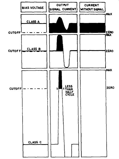
Figure A.1 Amplifier Operation
Class A amplifiers can be single-ended or pushpull, and can be used for both AF and RF.
Class AB1 operation requires a bias voltage somewhere between the cutoff voltage and the bias required for Class A. A somewhat larger input signal is required but its positive excursion, in the case of a vacuum tube, must not be large enough to draw grid current. Since the opposite excursion of the input signal goes a little beyond cutoff, output current drops to zero, so that the tip of the signal is clipped.
This results in some distortion, and it is preferable for this amplifier to be a pushpull type, so that the other tube or transistor can supply the missing portion. As a larger input signal is required, this amplifier is more suitable for a power output stage. It can be used for both RF and AF.
Class AB1 amplifier efficiency is better (25-35%) than Class A because less current is wasted in non-productive operation.
Class AB2 operation is similar to Class ABi, except that in vacuum tubes the input signal is allowed to be large enough to draw grid current on a positive excursion. The efficiency (35-50%) is better than Class AB1.
This is always a pushpull amplifier, and may be used for either RF or AF.
Class B operation requires a bias voltage at cutoff. This will give output-current low only on one half-cycle of the input signal, as shown in Figure A.1; therefore for audio it must always be used in a pushpull circuit. For RF it can be used with a single-ended circuit.
Since current in the absence of an input signal is negligible, efficiency is much higher (60-70% ), which is very important in higher-powered amplifiers.
Class C operation requires a bias voltage which may be two or three times the value of the cutoff voltage. Output current can low only during a portion of the alternate swings of the input signal, which there fore must be very large. However, as this portion is considerably less than a half-cycle the efficiency of a Class C amplifier is higher than any other (it may be over 90% ).
Class C amplifiers cannot be used for audio, and are mainly used for RF power stages in a transmitter. The output current lows in a series of powerful pulses that shock-excite the tank circuit into oscillation. As this is an LC resonant circuit its output waveform is a sine wave, varying in amplitude if modulated. Since the resonant circuit impedance is very high compared to that of the tube virtually all the output voltage appears across it.
Class C amplifiers can be either pushpull or single-ended. Because they are operated intermittently RF output power-amplifier tubes can be driven very much harder than if they had to run continuously.
Transistor Operation
You can think of a transistor as consisting of a pair of diodes joined back to back. A diode, whether germanium or silicon, comprises P-type and N-type " regions" which meet at a junction. To make a diode conduct, it must be forward-biased, which means that an external voltage has to be applied so that the P region is Positive with respect to the N region which, conversely, is Negative. The P region is the anode, and the N region is the cathode.
In Figure A.2 an NPN transistor (a) and a PNP transistor (b) are drawn as if they were pairs of diodes. In both transistors D2 is forward biased by B1, and D1 is reverse-biased by B2, consequently D2 should conduct and D1 should not.
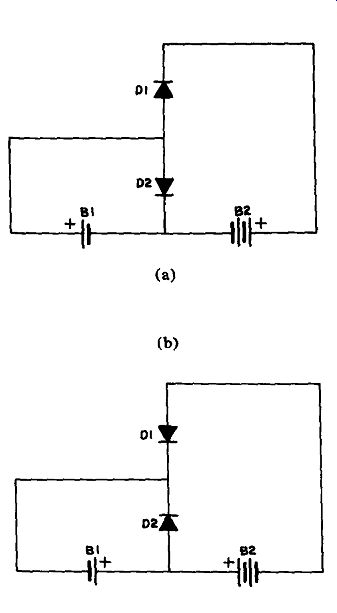
Figure A.2 Transistor Operation
Forward-biasing allows conduction by lowering the barrier voltage at the junction. Conversely, reverse-biasing raises it. However, because of the proximity of the junctions in a transistor, D1 is influenced by D2. Therefore when D2 is forward-biased both diodes conduct, and when D2 is reverse-biased neither does. Actually, the purpose of D1 is to increase the low of current from B2 through D1 and D2, so that amplification can take place, since a single diode cannot amplify.
In real circuits B1 is replaced by a voltage divider that drops B2’s voltage to the proper value. The forward-bias voltage required to over come the barrier at the emitter-base junction (D2 in Figure A.2) is .2 volt for germanium and .7 volt for silicon.
When a signal voltage is applied across the emitter-base junction it raises and lowers the barrier voltage in accordance with its own voltage fluctuations, thereby varying the current low through the transistor
The MOS/FET ("metal-oxide-silicon field-effect transistor") illustrated in Figure A.3 (also shown in a circuit in Figure 2.9) is made by oxidizing the surface of a thin wafer of N-type silicon. This oxide, which is a type of glass, is then removed from the source and drain areas by photo-etching. The wafer is then placed in a furnace in which a P-type impurity (boron, aluminum or gallium) is present as a gas that diffuses into the exposed areas, converting them to P-type silicon.
A similar process is used to deposit thin films of aluminum to form metal electrodes, and then gold wire leads are bonded to them by a combination of heat and pressure.
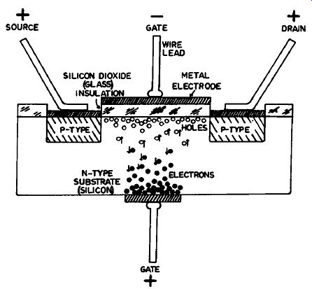
Figure A.3 MOS/FET
In this transistor the emitter, base and collector have been renamed source, gate and drain. There are actually two gate connections, one reinforcing the other.
The negative and positive voltages on the gate electrodes force electrons toward the lower gate, thereby creating a large number of holes.
These, having a positive charge, are repelled by the drain and low toward the source, because the drain's positive voltage is considerably higher than that of the source.
The actual amount of current lowing depends on the gate voltages, which force more or fewer electrons away, thereby making the path for the hole current wider or narrower. Consequently a signal voltage ap plied to the gate controls current low in the same way as it does in a vacuum tube.
This type of MOS/FET is called an enhancement type, because the low of current is enhanced by the gate voltage. Another type, which works in the opposite way, is called a depletion type.
The one illustrated in Figure A.3 is also called a P-channel device, because the N-type silicon substrate is actually converted to P-type when electrons are driven out of the region between the source and the drain. An N-channel device would be constructed with P-type substrate and N-type regions for source and drain. Current would be by electrons instead of holes.
Color Coding
Fixed non-metallic resistors and some other components are color coded to indicate their values instead of having the information printed or stamped on them. The colors used and their numerical significance are as follows:
Black 0 Brown 1 Red 2 Orange 3 Yellow 4 Green 5 Blue 6 Violet 7 Gray 8 White 9
On a composition resistor there are three or four colored bands around the resistor body, adjacent to one end. Starting with the one nearest the end, the first two colors are the significant figures of the resistor value in ohms, and the third is the power of ten of the multi plier. For example, blue (6), red (2) and yellow (4) should be read as 62 X 10<, or 620 kilohms. If the third band is gray (or silver), or white (or gold), the multiplier is 10"®, or 10" 1 , respectively.
If there is no fourth band the tolerance is ±20%. Otherwise, silver denotes ±10%, gold ±5%. Other tolerances may be indicated by using the applicable colors, but these are seldom encountered as most precision resistors have their values stamped or printed on them.
Some film-type resistors also may be color-coded, in which case an additional color may be added at the front end, to provide for three significant figures, followed by a multiplier and tolerance.
Capacitors, for the most part, are not color-coded. Exceptions are some ceramic and mica types. Ceramic tubular capacitors may be coded in the same way as composition resistors, except that an additional color is added in front of the others to indicate the temperature characteristic. The colored bands may also be replaced by colored dots.
Ceramic disks have these arranged around the edge, to be read clock wise. Some very small tubular capacitors have only three dots, which give two significant figures and the multiplier only.
Most mica capacitors are no longer color-coded. However, the lat rectangular molded silvered-mica type may employ an arrangement of six colored dots arranged three on each side of an arrow, or some other mark to indicate which way to read them. With the arrow pointing to the right the upper three dots (reading from left to right) indicate EIA standard (this is a white dot, which may be omitted) and two significant figures. The bottom row (reading from right to left) gives the multiplier, tolerance and type.
The significant figures always give the value in picofarads. The temperature characteristic (ceramic capacitors) or type (mica capacitors) is denoted as follows:
TEMPERATURE TYPE
COLOR CHARACTERISTIC (MFR'S SPEC.)
Black NPO A Brown N033 B Red N075 C
Orange N150 D Yellow N220 E Green N330
Blue N470 Violet N750 Diodes used in signal circuits are often color-coded because of their small size. Diode designations are always given, for example, in the form 1N914A. The IN- is common to all and does not have to be indicated, therefore the color bands denote the figures and letter following.
Suffix letters are coded as follows:
Black (no suffix) Brown A Red B Orange C Yellow D Green E Blue F Violet G Gray H White J The colored bands are grouped at the cathode end of the diode.
Transformer leads are color-coded as follows:
POWER TRANSFORMERS
Primary (tapped) Secondary Black (common) Black/yellow (centertap) Black/red or High voltage Primary (untapped) Two black leads Rectifier filament Amplifier filament # 1 Red Red/yellow (centertap) Red Yellow Yellow/blue 1 (centertap) Yellow Green Green/yellow (centertap) Green
Primary Blue (plate) Red (B+) Amplifier filament #2 Brown Brown/yellow (centertap) Brown
-
Slate Amplifier filament #3 -
.Slate IF TRANSFORMERS Secondary Green (grid or diode) Green/black (full-wave diode) Black (grid or diode return, AVC or ground) AUDIO & OUTPUT TRANSFORMERS Primary Blue (plate) Red (B+)
* Blue or brown (plate) Secondary Green (grid or voice coil) Black (return or voice coil) " Green or yellow (grid) *
Pushpull only.
Preferred Values
Most resistors and capacitors other than precision or special-buy items are supplied in preferred values, to simplify manufacture and stocking by limiting the number of different values to bare essentials.
The tolerance provides the necessary spread to cover the gaps between the nominal values. Preferred values for the three principal tolerances are manufactured for each multiplier as follows:
International System of Units (SI Units) Standard units of measurement have been adopted by most countries, and in electronic work those listed below with their symbols are now in general use.
Physical Quantity SI Unit Symbol Old Name & Symbol (if different) Current ampere A a, amp Capacitance farad F f ,
fd Inductance henry H h Frequency hertz Hz Cycles c, cps Cycles per second Wavelength meter m Resistance ohm o
Time second s sec
Voltage, potential difference, electromotive force volt V v
Power watt W w
Standard prefixes that are used with the above to obtain units of convenient size are as follows:
-------------------