THIS SECTION COULD WELL have been titled "miscellaneous” for in it we deal with circuits which do not it into any of the categories covered in previous sections.
MULTIVIBRATORS
A multivibrator is a circuit in which a pair of vacuum-tube or transistor switches turn each other alternately on and off. There are three types:
Astable multivibrators are RC relaxation oscillators and, as such, are discussed in section 4. They may also be called free-running multivibrators.
Monostable multivibrators are the electronic equivalent of push button switches. As soon as the input signal is removed they return to their normal state. They are also known as single-shot multivibrators.
Bistable multivibrators are the electronic equivalent of double throw switches. They require a second input signal to return them to their first state. Bistable multivibrators are also called lip-lops, or binary counters.
MONOSTABLE MULTIVIBRATORS
The monostable or single-shot multivibrator will be considered first.
With this type an output is produced whenever the proper input signal is received.
Distinguishing Features
Figure 12.1 is the same plate-coupled free-running multivibrator that was illustrated in Figure 4.12. Figure 12.2 is a single-shot multi vibrator, also employing a dual-triode tube.
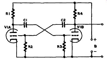
Figure 12.1 Astable or Free-Running Multivibrator
Note that the only important difference between them is the absence of the feedback connection in the single-shot version. In Figure 12.1 this connects the plate of V1B via C2 to the grid of V1A.
It is true that the single-shot multivibrator is shown with an input connected across R2, while the free-running multivibrator does not have one, but as you can see by looking at Figure 4.14 the oscillator type may also have an input.
In Figure 12.2 a cathode resistor has also been added.
Use
This circuit is designed to produce an output pulse with a specified duration and amplitude from an input of any shape, provided it has the proper polarity and voltage to trigger the device.
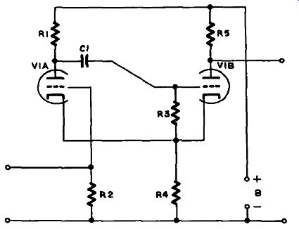
Figure 12.2 Monostable or Single-Shot Multivibrator
Detailed Analysis DC Subcircuit: In the absence of any input signal, electron low is from B- via R4 to both cathodes, and from V1A's plate via R1, and V1B's plate via R5, back to B+. Since R3 connects the grid of V1B to the upper end of R4 the grid is not biased by the voltage drop across R4, and consequently the grid voltage is essentially the same as the cathode voltage. Therefore V1B is conducting, and its plate voltage is lower than the supply voltage by the value dropped across R5.
However, the grid of V1A is connected to B- via R2, therefore this tube is biased negatively by the voltage drop across R4, and is cut of.
The plate voltage of V1A is therefore equal to the supply voltage, and capacitor C1 is also charged to the same value on the side toward V1A.
AC Subcircuit: When a positive trigger pulse is applied across R2 of sufficient amplitude to overcome the negative bias on V1A and allow the tube to conduct, there is an immediate voltage drop across R1, and this sends a negative-going pulse through C1 to the grid of V1B. V1B now ceases to conduct, and its plate voltage rises to the value of the supply voltage.
After the trigger pulse, V1A returns to its non-conducing state and its plate voltage returns to the supply voltage level.
The rise in positive voltage is coupled through C1 to the grid of V1B, and this tube resumes conduction.
The length of time V1B is off, and hence the duration of the output pulse, is determined by the R-C constant of C1 and the resistors R1, R3 and R4, in series across the supply voltage.
SCHMITT TRIGGER
The Schmitt trigger (Figure 12.3) is a variation of the preceding circuit, and illustrates a typical transistor single-shot multivibrator.
Like the vacuum-tube version, it requires an input trigger of proper polarity and voltage, and produces an output of fixed amplitude and duration, determined by the circuit constants. R2 is connected in parallel with C1 to complete a voltage divider, R1, R2 and R5, that stabilizes the base voltage of Q2, which is normally conducting, since its base is more positive than its emitter. Q1 is normally not conducting since the top of R4, though less positive than Q2' s base, makes Q1's emitter positive with respect to Q1's base, which is connected to zero potential via R3. The operation of the circuit when a positive input pulse turns Q1 on is the same as for the vacuum-tube circuit.
BISTABLE MULTIVIBRATOR, OR FLIP-FLOP
Figure 12.4 shows an Eccles-Jordan lip-lop circuit which is typical of bistable multivibrators.
Distinguishing Features
In this circuit it appears as if the feedback connection of Figure 12.1, removed in Figure 12.2, has been restored. However, the presence of the two diodes indicates that this circuit is not really a free-running multivibrator despite appearances. These diodes form a steering circuit that directs the input to each transistor in turn, so we have actually two single-shot multivibrators. If Q1 is of and Q2 on, the input goes to Q1, which then turns on while Q2 turns of. The next pulse is then steered to Q2, turning it back on, and Q2 is turned of again.
Uses
Counters, computers and industrial controls.
Detailed Analysis
Q1's collector is connected to a voltage divider consisting of R2, R3 and R5. Q2' s collector is connected to one consisting of R7, R6 and R4. When Q1 is turned of the supply voltage is divided between R2, R3 and R5, so that the collector of Q1 and the base of Q2 are both negative with respect to the emitters. Q2 therefore has forward bias and turns on; consequently the voltage on the collector is zero, while Q1, with zero bias, remains turned of.
Diode D1 also has zero voltage on the cathode, but a negative voltage reaches its anode via R1. D2 has a negative voltage on its cathode but no voltage on its anode, which is connected to Q2’s collector via R8, Consequently D1 is turned of but D2 is on.
If a positive pulse appears at the input it goes to both diodes, but as only D2 is conducting, it only reaches Q2' s base. Here it overcomes the negative bias on the base, and causes Q2 to turn of. As a result its collector voltage rises, and the negative-going change in the voltage is coupled through to Q1's base, turning Q1 on. Q1's collector voltage drops to zero, carrying Q2's base voltage to zero also, so the two transistors are now in exactly the opposite state from when the input pulse arrived. Since Q2's collector voltage has now risen from zero to a substantial proportion of the supply voltage, a negative voltage now appears at the output.
The bias on the two diodes is now the opposite of what it was before.
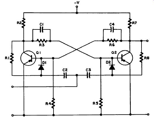
Figure 12.4 Bistable Multivibrator, or Flip-Flop
Consequently, the next trigger pulse will be steered to Q1's base. Since Q1 is now in the identical state that Q2 was in, while Q2 is now in Q1's former state, Q1 now turns off, turning Q2 on again, and Q2's collector voltage now becomes zero once more.
The speed at which this circuit can switch depends upon the values of R1-C2 and R8-C3. Both resistors and capacitors cannot be very small values, or the input pulse will not be able to switch the transistor, but will appear at the output. Speed can be improved by connecting diodes parallel with R1 and R8.
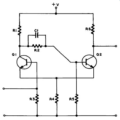
Figure 12.3 Schmitt Trigger
Another method is to remove R1-C2, R8-C3 and both D1 and D2.
The emitters are connected together, and a resistor placed between them and the low side of the circuit (like R4 in Figure 12.3). The input pulse is then applied across this resistor. It momentarily interrupts the current low in the "on" transistor by reversing the bias. This type of bistable multivibrator is called emitter-triggered. Another type is collector-triggered. However, the Eccles-Jordan type is the most widely used.
SAWTOOTH GENERATOR
In section 4 the use of relaxation oscillators for the generation of sawtooth waveforms was discussed. However, certain applications re quire a more linear sawtooth than these can produce. Figure 12.5 shows such a type.
Distinguishing Features
R2, R3 and C1 form a timing circuit in which R3 and C1 are usually two of a set of resistors and capacitors that can be switched in and out of the circuit to obtain different sawtooth slope speeds. R2 is a calibration adjustment. The circuit may employ all tubes or all transistors, or both, as shown.
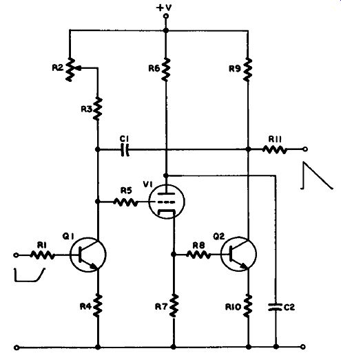
Figure 12.5
Uses
Mostly used in oscilloscope sweep generators.
Detailed Analysis
The input to this circuit usually comes from a single-shot multi vibrator, such as a Schmitt trigger, so that each sawtooth wave is triggered reliably, not from random pulses or noise spikes.
The proper pulse arrives on the base of Q1, which is called the disconnect amplifier (sometimes a diode is used).
This transistor is normally conducting, and current lows up the path R4, Q1, R3 and R2 to the positive side of the supply voltage. This voltage divider maintains a constant voltage on the grid of V1 which is slightly negative relative to its cathode, but not enough to cut it of.
When Q1 switches of, this situation changes. The voltage on Q1's collector now starts to rise toward the value of the supply voltage. The rate of this rise is controlled by the R3-C1 combination,
since the capacitor can only charge at the R-C time-constant of the two.
As the voltage rises the tube's conduction increases. The current through R7 increases, and the voltage drop across it increases. Consequently the base of Q2 goes more positive.
This results in Q2*s conductance increasing in similar proportion, so that its collector voltage goes down.
This negative-going voltage is fed back to the grid of V1 via C1, and tends to oppose the rising positive grid voltage, thus maintaining a linear rise in this voltage, so that a linear output waveform is obtained.
A feedback from the output to the Schmitt trigger (not shown) turns it off at the end of the ramp, and it turns Q1 back on by removal of the pulse on its base. This places the circuit in readiness for the next trigger pulse to start the next sweep.
FREQUENCY DIVIDER
Figure 12.6 illustrates a typical frequency divider, in which an output pulse is produced only after a certain number of input pulses have been received. For example, if it takes six input pulses to produce one output pulse, the output frequency is only one-sixth of the input frequency.
Distinguishing Features
In this circuit the three-winding transformer connected between the plate and grid of V1 is distinctive, especially when taken in conjunction with the two diodes in the input and the positive voltage applied to the cathode from the variable resistor R2, which, with R1, forms a voltage divider between B+ and the low side of the circuit.
Uses
Counters and similar applications.
Detailed Analysis
V1 is biased beyond cutoff by the positive voltage on the cathode, which can be adjusted by R2.
When a positive-going pulse arrives at the input it is coupled through C1 and D2 to C2. Any negative-going portions of the pulse are by passed by D1. C1 charges up slightly, but cannot charge more because the pulse does not last long enough. However, the charge cannot leak away because D2 cannot conduct in the other direction, and V1 is cut of.
Successive pulses gradually build up the charge on C2 until the voltage on V1's grid reaches the level where the tube can conduct. V1 becomes a low impedance, discharging C2 and dropping the plate voltage. As soon as C2 discharges, however, the tube cuts of again, the plate voltage rises to its former value, and the cycle is repeated.
Figure 12.6 Frequency Divider
Circuit Variations
Instead of a three-winding transformer, one with two windings only may be used in conjunction with a dual-triode tube in which one triode replaces the third winding. Both grids and cathodes are connected together. When the first triode conducts, the second does so also, producing an output pulse in the same way as the third winding of the transformer in the previous example.
Thyratrons or silicon-controlled rectifiers may also be used instead of triodes, but since they do not stop conducting under the same conditions as a tube, slightly different circuit arrangements will be required (see section 7 ).
FREQUENCY MULTIPLICATION
The broadcast frequency of a radio station may be many times that of the master oscillator, as we saw in section 4. The carrier frequency may be doubled by using the circuit of Figure 12.7. Several stages in succession ( " cascaded" ) will multiply it as many times as necessary.
Distinguishing Features
This circuit is basically the same as that of Figure 3.10, which was a Class C RF power amplifier. The only real difference is that there is no neutralizing capacitor in Figure 12.7.
Uses
Transmitters.
Detailed Circuit Analysis
This RF power amplifier was discussed in section 3, so we need not go over its operation as an amplifier again. The input resonant circuit L2-C1 is tuned to the frequency of the signal from the previous stage.
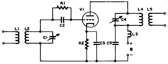
Figure 12.7 Frequency Doubler
The output tank circuit L3-C4 is tuned to double this frequency.
The tube generates harmonics of the fundamental frequency, and the second, which is double the fundamental, makes the output tank oscillate. In a circuit where the output and the input are at the same frequency this harmonic will be much attenuated, because the output tank is not tuned to that frequency.
Since the output frequency is not the same as the input, oscillation caused by feedback is not as much of a problem, and feedback neutralization is not usually required.
The frequency comparator circuit in Figure 12.8 is similar to the discriminator circuit of Figure 6.7 used in FM receivers.
Distinguishing Features
This circuit only differs from a discriminator in having T2 separate, and not a part of T1.
Use of a discriminator to control frequency was mentioned in connection with FM modulation in section 5. Such a discriminator operates as a frequency comparator. The circuit may be used in any application where automatic frequency control is required.
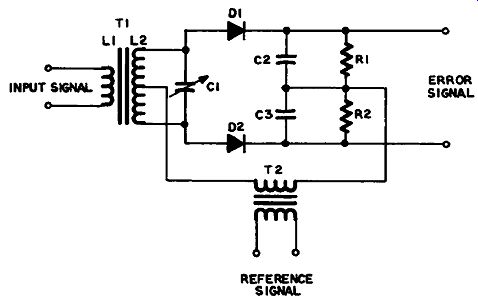
Figure 12.8 Frequency Comparator
Detailed Analysis
A control or standard frequency from a crystal-controlled oscillator is coupled into the circuit through T2. A sample of the signal to be monitored is applied across T1.
The operation of the circuit is the same as the operation of the discriminator (see section 6). As long as no difference exists between the input signal and the reference signal the voltages at each end of L2 remain equal, consequently the charges on C2 and C3 are equal also. Since they cancel each other no output voltage is produced.
When the input signal changes so that it is no longer at the resonant frequency of L2-C1 the two halves of L2 develop different voltages due to the resultant phase shifts. C2 and C3 are now charged to different voltages, so an error voltage appears at the output. This error voltage may be used to correct the signal frequency by using a reactance circuit, as explained in section 5.
PHOTOCELLS
Transducers are devices for converting physical quantities of one kind into corresponding physical quantities of another kind. A loud speaker changes electrical signals into sound waves, a microphone changes sound waves into electrical signals.
Transducers which do the same for light are also of two kinds:
1. Photosensitive, changing light energy to electrical energy.
2. Photoemissive, changing electrical energy to light energy.
Photosensitive devices are also of two main types:
1. Photovoltaic, generating a voltage; and 2. Photoconductive, allowing current to pass.
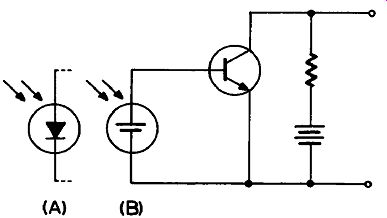
Figure 12.9 Photovoltaic Transducers
Figure 12.9 illustrates a photovoltaic transducer or photocell (B) connected in a circuit in which the voltage produced by light falling on it controls a transistor, which amplifies it. Note that the symbol for the photocell is that of a voltaic cell enclosed in a circle, with arrows pointing towards it to represent incident light. The older device was a phototube, and a similar vacuum-tube circuit was used in automobiles for automatic dipping of the headlights. A rather more elaborate circuit is used for "reading" the sound track on the edge of a motion picture film and converting it to an audio signal.
The solar cell used in solar batteries is also a photovoltaic device, though the idea here is simply to generate power, not to drive an amplifier.
The other device, illustrated at (A), is a photodiode, which changes from non-conduction to conduction under the influence of light.
Figure 12.10 illustrates a photoconductive device (a cadmium sulfide photocell) as used in a modern camera. In this circuit the resistance of the cell varies with the intensity of light falling on it (reflected from the scene viewed by the camera), so that the reading of the exposure meter E, which depends on the battery current passed by the cell, indicates the light value. A variable resistor allows the current to be adjusted to bring the meter pointer or other indicating device back to midscale or some other index, to compensate for different film speeds, lens apertures, and so on. In some cameras this is done automatically.
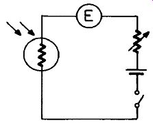
Figure 12.10 Photoconductive Transducer
Lamps of all kinds are the most well-known photoemissive devices, but a more recent development is that of light-emitting diodes (LEDs), which because of their small size and low current consumption can replace lamps with advantage in many applications, especially as indicators and in readout displays. It is possible that they may also one day be used for TV screens.
CATHODE-FOLLOWER CIRCUIT
Figure 12.11 illustrates a cathode-follower circuit, which is a special type of amplifier circuit having a voltage gain of less than unity, though there may be a power gain.
Distinguishing Features
The cathode-follower circuit has the same features as the voltage amplifiers of section 2, except that:
1. The plate is grounded for signals through C2.
2. The output is taken from across R2.
3. There is no cathode-bypass capacitor.
Uses
This circuit is used to couple a high impedance to a lower without the frequency losses inherent in the use of a stepdown transformer.
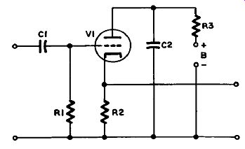
Figure 12.11 Cathode Follower
Detailed Analysis
DC Subcircuit: Electron flow is from B- via R2, V1 and R3 back to B+. R2 provides grid bias by making the cathode more positive than the grid because of the voltage drop across the resistor, and R3 drops the B+ voltage to the correct operating value for the plate.
AC Input Circuit: Input signals are applied between grid and cathode of V1 as in other amplifiers, and using standard types of coupling from the previous circuit. This example is RC-coupled via C1 and R1.
AC Output Circuit: Variations in signal voltage on the grid of V1 cause corresponding variations in the resistance of the tube and, there fore, in the current lowing through it and through R2. Since R2 is not bypassed an output signal voltage appears across it. No output signal appears across R3 because it is bypassed by C2. The output signal is in phase with the input, which it is therefore said to "follow." However, the absence of a cathode-bypass capacitor introduces degeneration (see section 2), which is why there is a voltage loss with this circuit instead of amplification.
Circuit Variations
Figure 12.12 gives the transistor equivalent of Figure 12.11. This circuit is called a grounded-collector circuit, because the collector of Q1 is bypassed by C1, so that no signal voltage develops across R1.
The output is taken from R2, therefore, which is not bypassed. The output signal is in phase with the input.
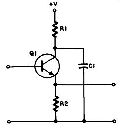
Figure 12.12 Grounded Collector Circuit
-------------------