A collection of eighteen projects that will add spice to your project building pleasure!
CONTENTS
(Part 1)
1. TWINKLE TREE
2. ONE-SECOND FLASHER
3. 5-VOLT POWER SUPPLY
4. SOUND–SWITCH
5. LIGHT ALARM
6. SIG-TRACER
7. CW FILTER
8. VOL-EXPANDER
9. COMPUTER VOICE
10. AUDIO POWER BOOSTER
(Part 2)
INTRODUCTION
Building projects is fun! Exactly where the most fun is can be debated. Is it in the actual assembly of the gadget? What about designing added features or molding it to particular needs? How about watching friends and family "pop eyes" as you exhibit its operation? Who knows? Never examine a pleasure, just enjoy it! With that admonition, inspect the plans of the seventeen projects presented in this Project Anthology while you heat up your soldering iron.
The experience level required of the project builder is minimal. Of course you require some level of project building experience but every effort has been made to keep the level of difficulty down. In some projects the illustrations go beyond the schematic diagram to include mechanical layout information. Although your electronic theory understanding may be scant, you will require higher levels should you indulge in designing additional functions and features into the projects presented herein.
Here are general notes about the parts used in projects.
Resistors. Fixed-valued resistors are rated at either 1/4-watt or 1/2-watt, within 5 percent of their designated value. One-half watt is the preferred rating for resistors because of their physical size and ease of handling on circuit boards. Hobbyists with construction experience should select the wattage size that they deem suitable for the project. Resistors that are specified with wattage ratings may be substituted for other resistors of higher wattage rating. For example: you could replace a 1-watt resistor with a 3-watt resistor provided that the replacement is not of wire-wound construction. Wire-wound resistors have a measure of inductance in them and they may upset the operation of the circuit, especially high-frequency audio and radio circuits. The physical size of the resistor increases significantly with its power rating so common sense directs that you do not use outlandish substitutions.
Only composition resistors are used in the following projects. Do not substitute different ohmic values unless the text discusses the possibility, or you are thoroughly qualified to make ohmic value changes by adequate academic knowledge and/or experience.
Capacitors. The voltage ratings of capacitors in the projects should be equal to or above that specified in the Parts List. Electrolytic capacitors should be reasonably close to the specified value in micro-Farads. The working-voltage-DC (WVDC) rating must never be less than specified, and as a rule never more than twice the specified rating. Two capacitors connected in parallel add their values. Two capacitors, say .10-uF and .25-uF in rating, when connected in parallel will be equal to a single capacitor rated at 0.35 uF. When paralleling capacitors to obtain useable values, be sure that the WVDC ratings of both capacitors are at least equal to the specified value.
Semiconductors. Solid-state parts such as transistors, integrated circuit chips, diodes, LEDs, etc., cause the most problems for new project builders. It is recommended that they obtain catalogs from retail and mail-order outlets. Radio Shack is an excellent retail source-there's one in every town in North America that has more than two traffic lights, or so it seems. There are a host of parts advertisers who offer free 800 telephone numbers so you can do your shopping at home. Some readers resort to substitution listings for what appears to be hard-to-get parts. This could be risky for beginners because pin connections vary with so-called identical units. If you are calling an 800 telephone number parts outlet, insist upon the exact part. There are enough 800 electronic parts suppliers in North America to call and get the parts you want.
Light-emitting diodes (LEDs) usually have their cathodes identified by the shorter lead which is closest to the flat edge of the circular rim at the base of the part. There are variances, and for bi-color LEDs, this is true for one of the colors only. If you have any doubts, do not hard solder the LED into the circuit at first. Run a power-on test and if the LED does not light, or the wrong color comes up, reverse the leads and try again. The LED should light or the correct color appear. Now you can solder the LED into the circuit. Solderless circuit boards can be used for testing mockups.
Not every construction or parts problem can be forecasted, however, experience is a great teacher and you will learn much by jumping into the construction of a simple project. Experience grows with practice. The fantasies of the Project Anthology are now all yours to enjoy. Have fun!
THE PROJECTS
1. Twinkle Tree
Twinkle Tree is an easy project for beginners to build, and its basic circuit has a number of useful applications. The circuit's visible action appears as a string of ten LEDs (light-emitting diodes) flashing on one at a time in sequence, this being repeated so long as the circuit is powered.
Fig.
1--Circuit diagram for the Twinkle Tree project.
======
PARTS LIST FOR TWINKLE TREE
Semiconductors
D1-1N4001 rectifier 101-7490, decade counter (divide by 2 and 5)
IC2-7441, 1BCD-to-decimal decoder
LED1-LED10-Light-emitting diode, color optional Tr1, Tr2-2N3706, PNP ZD1-5.1-volt, 400-11A Zener diode
Resistors
R1-2,200-ohm R2, R3-33,000-ohm R4-1,000-ohm R5-220-ohm R6-33-ohm, 1/2-watt
Capacitors
C1, C2-2-µF, 6-WVDC, electrolytic C3-47-nF or .05-uF, metallized polyester C4-1,000-µF, 12-WVDC, electrolytic
Miscellaneous
T1-Filament transformer: 117-volt AC primary winding, 6.3-volt AC secondary winding (obtain smallest, lowest power unit available)
On/Off switch optional, 14-pin and 16-pin IC sockets, pert-board, wire, battery clip (optional), solder.
======
The LEDs can be used on a small table deco ration, in the form of a Christmas tree (we call it Twinkle Tree), or around a picture frame; or they may be placed at various points on a hanging decoration, such as a bunch of mistletoe, or can be incorporated in other decorations or models.
The LED light display provides an interesting and novel twinkling effect.
The same circuit can be used with the LEDs placed round a small display, so that they flash on in turn with a revolving or racing effect.
How It Works. Figure 1 is the schematic diagram of the circuit for Twinkle Tree which includes a small power supply for operation from AC lines. If the circuit is to be powered from an existing supply, or batteries, omit circuit components ZD1, D1, R6, C4 and T1 . The external power supply negative line goes to the "E line in Fig. 1, and the positive line to the junction of resistors R1 through R5. The voltage sup plied should be approximately 5-volts DC. You may want to connect an AC wall-plug power pack rated at 5-volts DC as the power source. Do not use 6-volt DC from dry cells or else the ICs will be damaged. 4.5-volt DC from three 1.5-volt dry cells may be used, however the LEDs will appear to be a bit dimmer.
The multivibrator circuit consists of transistors Tr1 and Tr2 which produces pulses that form the input to the binary-coded, decimal-decade counter IC1, at pin 14. This IC counts the pulses and provides a binary output at 1-12, 9, 8 and 11 pins. Pin 5 is its positive line, and 10 is its negative line.
With counters having two or more numerals, as shown later, the IC can pass on a pulse to the "tens" section. Here, it is used alone and repeats the same series of outputs over and over so long as the multivibrator pulses are applied to pin 14.
Chip IC2 is a decoder-driver. Its purpose is to receive the various inputs at 3, 6, 7 and 4, and decode them into outputs at 16, 15, 8, 9 and so on, along to 1 and 2. Thus each of these ten points provides a circuit to the appropriate LED in turn.
The outputs connected to LEDs are located at the top of IC2 when Fig. 1 is held right-reading.
All the LEDs are returned through the common limiting resistor R5, to operate from the same 5-volt DC line. The effect is, that each LED is illuminated in turn, along the line, and when the last is reached, this is followed by the first, and the sequence is repeated. Check the LED polarity, and mark this with red sleeving material, or other means, if the LEDs have no means of identification (long lead or flat side).
For the Twinkle Tree the ten LEDs are scattered at random, and any LED could be connected to any of the outputs 16 to 2.
Only one LED is on at a time, so current drain is only some 50 mA or so, and this small current load makes battery operation feasible and long lasting.
Transformer Ti (6.3-volt AC secondary) provides about 9-volt peak across C4, and R6 drops this for the 5.1-volt DC Zener diode ZD1. A meter placed across this diode should read about this voltage.
AC line current is drawn from a 3-pin power-plug line cord with a 2A built-in fuse. The green lead ground circuit in the power cord provides safe grounding of the secondary and low-voltage circuit. A double-insulated transformer specified as requiring no grounding may be operated with out grounding through the AC power cord's green lead. Nevertheless, always play safe by using a ground circuit whenever using the AC line. Naturally construction and wiring must assure that no AC voltages can reach the trans formed secondary output or the low-voltage circuit.
Construction. This is where the fun in electronics begins. Design your own Twinkle Tree.
Maybe you would want to add a few fixed (always-on) LEDs or build two circuit boards and have twice as many twinkling lights. It's up to you!
2. One-Second Flasher
Fig. 2--Circuit diagram for the One-Second Flasher.
When making a long exposure using a camera with the shutter set to "B or "T", some sort of timer is needed in order to obtain accurate results.
Unless very long exposures are required, a simple one-second indicator such as the One-Second Flasher is probably the ideal solution. The unit pulses on a LED (light-emitting diode) indicator at one second intervals. The shutter is opened as the LED flashes, and then closed after the appropriate number of flashes have been counted off.
There are almost certainly a great many other uses for a simple timer of this type, and it could be used as a simple enlarger timer for example. How It Works. The circuit diagram for the One-Second Flasher appears in Fig. 2, and is based on an operational amplifier that is biased by R1, R2 and R3 to act as a form of Schmitt trigger. The output goes to the low state if the inverting input is taken about 2/3V+, and high if it is taken below 1/3V+. The output therefore goes high initially, but C2 soon charges to 2/3V+ via R4, and then the output goes low. Capacitor C2 then discharges to 1/3V+ via R4, sending the output high again, and producing continuous oscillation.
Resistor R4 is adjusted to give an operating frequency of one Hertz. The One-Second Flasher can be calibrated against a watch or clock with a seconds hand by empirical means. The output of IC1 is coupled to the LED indicator, D1, by way of DC blocking capacitor C3 and current limiting resistor R5, and the LED is briefly pulsed on as the output voltage swings positive. Diode D2 ensures that there is both a charge and discharge path for C3 so that the output signal is properly coupled to D1.
The current consumption of the unit is about 2 mA.
As You Like It. Assembly and packaging of the unit is left to the builder. The circuit can be housed in a plastic cassette holder. The LED need not protrude because the case is clear. The circuit uses very little current so that a 9-volt transistor-radio battery can be used. The battery can be disconnected by unsnapping the clip connector or adding a single-pole, single-throw slide switch.
PARTS LIST FOR ONE-SECOND FLASHER
Semiconductors:
D1-Light-emitting diode, red
D2-1N4001 rectifier
IC1-LF351 operational amplifier
Resistors:
R1-R3-100,000-ohm
R4-220,000-ohm trimmer
R5-470-ohm
Capacitors
C1-100-nF, metallized polyester
C2-C3-10-µF, electrolytic
Additional Parts & Materials
S1-S.p.s.t. slide switch
Plastic cassette holder, 9-volt transistor-radio battery, wire, perfboard, solder, etc.
3. 5-Volt Power Supply
Fig. 3--Circuit diagram for the 5-Volt Power Supply.
Fig. 4--Parts layout for the 5-Volt Power Supply. Observe markings on the
diodes (D1 and D2) when soldering to the terminal strip
The series of 7400 TTL integrated circuits are intended to operate from a 5-volt DC supply as are many other modern chips, and integrated circuit voltage regulators for this purpose are avail able.
The 5-Volt Power Supply shown here will provide voltage-regulated power for digital ICs needing up to 500 mA. By constructing the 5 Volt Power Supply as a separate unit, any circuit to be operated can be plugged in, and this allows it to provide power for various projects. It may also be used where a 5-volt DC, 500 mA supply is suitable, so it can in some cases be pressed into service where a 4.5-volt or 6-volt battery would otherwise be fitted.
The Circuit. Figure 3 shows the schematic diagram for the circuit. Transformer T1 provides isolation from the AC power line, and has a 9-0 9-volt, 500-mA secondary winding. After rectification, the DC input voltage for IC1 is something over 9-volts. A filament transformer rated at 12-0-12-volts AC may be substituted.
Diode rectifiers D1 and D2 are rated at 50 volts at 1 A: These diodes are readily available.
Capacitor C 1 helps suppress transients arising from the AC line, and C2 is the main smoothing (filtering) capacitor. Here, a value of 1500-µF to 3500-tiF may be used. Higher capacitances provide better voltage-ripple smoothing.
Chip IC1 is the LM341, a 5-volt, 500-mA positive regulator. Actual maximum current depends to some extent on other factors. Here, heat sinking is to a small metal chassis.
========
PARTS LIST FOR 5-VOLT POWER SUPPLY
Semiconductors:
IC1-LM341 voltage regulator chip
D1, D2-1N4001 rectifier
Capacitors:
50-WVDC, electrolytic
C2-3500-µF, 16-WVDC, electrolytic
C3-0.1-RF, 50-WVDC, polyester
Additional Parts & Materials
S1--S.p.s.t., toggle switch
T1-120-volt/9-0-9-volt, 500-mA power transformer
Aluminum chassis box, 3-conductor power cord with molded plug and built-in fuse holder, 2 A fuse, 1 terminal strip with a minimum of 4 insulated ties and 2 grounded ties, 1 terminal strip with a minimum of 2 insulated ties and 1 grounded tie, wire, solder, 2 output connectors, red and black (binding posts preferred), etc.
==========
Figure 4 shows layout inside a small metal- box chassis. This can be a 4 X 6-in. chassis with enough height to clear the top of the transformer, T1. Follow the layout in the diagram when assembling the project to avoid errors.
Safety. The AC line power cord has three leads, green for ground or earth (E), white for neutral (N), and black for live (L) conductors. A thin power cord (#18 gauge) is adequate. Use a 3-pin fused plug, and place a low-rating fuse of 2A or 3A in this.
The cord passes through a rubber grommet, and its conductors are anchored on the 3-way terminal strip. Note that the switch Si is placed in the live conductor (L) lead. The earth (E) lead (usually green in color) is connected to the chassis. This is also connected to the trans former core, and to the output negative line. If this lead is omitted and the negative return provided by the chassis is to be relied upon, be sure the attaching screws are very tight, and will not become loose.
The grounding is for safety. If a short circuit should arise in Ti or elsewhere, which could carry AC line voltages to the chassis and low-voltage output circuit, the low-rating fuse in the plug will blow.
The unit needs to be enclosed in an aluminum chassis box or case, so that no hot AC leads can be touched.
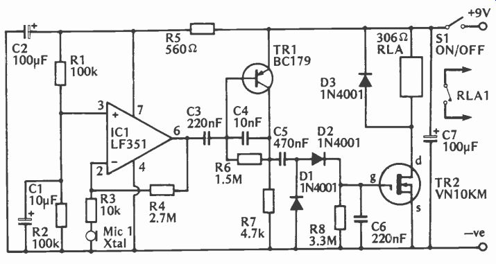
Fig. 5--The circuit diagram for the Sound Switch project.
Safety, with this unit and similar AC line-operated power supplies, depends upon sound construction, correct wiring, fusing and grounding, and shielding of high-voltage points against accidental contact by the user. No high voltage must ever be able to arise on the low-voltage output sockets, or low-voltage wiring as equipment connected to the unit will no longer be safe to touch.
Testing. A DC voltmeter should show approximately 5-volts at the output terminals. Due to tolerances in IC1, and lack of exact accuracy of the meter, the reading might be very slightly above or below 5-volts.
To check for regulation, connect a load taking up to about 500 mA. A 6.3-volt, 0.3 A or 3-watt light bulb is suitable. The reading at the output sockets should remain virtually unchanged.
4. Sound-Switch
The Sound-Switch circuit of Fig. 5 is suitable for use in a sound-activated tape recorder and similar voice-activated applications. Provided a reasonably sensitive crystal microphone is used, the unit will operate from speech of normal volume at a range of several feet. To go beyond that range will invite the rustling of paper, coughs, heel clicks, crowd and traffic noises, air conditioner noise, and many other room and out-of door noises that will obviate the need of Sound-Switch. A too sensitive sound activated switch would be on most of the time when placed in a noisy environment and a super sensitive microphone used to increase range would be worthless.
=========
PARTS LIST FOR SOUND-SWITCH
Semiconductors:
D1, D2-1N4001 rectifier
IC1-LF351 operational amplifier
Tr1-BC179 or 2N3965 , silicon PNP transistor
Tr2--VN1OKM
Resistors
R1, R2-100,000 –ohm
R3--10,000-ohm
R4--2.7-Megohm R5-560 –ohm
R6--1.5-Megohm R7-4,700 –ohm
R8--3.3-Megohm Capacitors
C1--10-µF, electrolytic
C2, C7--100-µF, electrolytic
C3-220-nF, metallized polyester
C4--10-nF, metallized polyester
C5--470-nF, metallized polyester
C6--220-nF, metallized polyester
Additional Parts & Materials
Mid-Crystal microphone
RLA--Relay with DC coil resistance of 306–ohms
Plastic or aluminum case, 9-volt battery (see text), wire, solder, etc.
=========
How It Works. The circuit uses IC1 as a low-noise preamplifier having a voltage gain of 270 times, and this is followed by a second stage of amplification which gives a similar voltage gain.
The second stage uses Tr 1 in the common-emitter mode and this is a conventional arrangement except for the inclusion of C4. This capacitor provides a considerable amount of high-frequency attenuation, and this is necessary in order to prevent instability. Capacitor C5 couples the greatly amplified output of Tr1 to a rectifier and smoothing circuit which gives a positive DC output signal which is roughly proportional to the input signal level. If the input signal is sufficiently strong, the bias voltage at the gate of VMOS device Tr2 will be adequate to bias this transistor into conduction, and the relay which forms its drain load is then activated.
A pair of normally open relay contacts are used to control whatever item of equipment is operated by the unit. Of course, the voltage at the gate of Tr2 soon decays as C6 discharges through R8 if the input signal ceases, and the relay is then switched off. The decay time is roughly one second, which is about the optimum time for most applications. The attack time of the circuit is only a fraction of a second, and the unit responds almost immediately when a sound is initially picked up by the microphone.
Using It. You may want to record your voice giving instructions or reports, such as announcing the disassembly of a complicated component.
As you speak, imitate the police and military who use such equipment. Begin each sentence with the word, "Kay." For example, "Kay. Removing the pawl from the gimbals." On playback, all your important words are not clipped and you have an accurate disassembly procedure that can be reversed for assembly purposes.
As the circuit has a fairly high level of gain the component layout must be designed with reason able care, although the very limited bandwidth of the circuit greatly reduces the risk of instability.
The current consumption of the unit is about 3 mA under quiescent conditions, but this increases considerably when the relay is activated. The circuit may be operated from a 9-volt transistor-radio battery, but you may want to use six C cells in series or a wall-plug power pack.
5. LIGHT ALARM
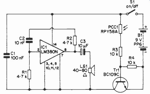
Fig. 6--The circuit diagram of the Light Alarm.
The Light Alarm unit produces a noticeable audio tone when the unit's photocell is subjected to a reasonably high level of light; normal day light and artificial room lighting are sufficient to operate the circuit. The Light Alarm could be used as a simple burglar deterrent, and it would then be placed in a cabinet or a drawer, and would produce the alarm signal if the cabinet or drawer was opened by a burglar. The sudden noise would hopefully unnerve him or her sufficiently to make them leave the premises immediately. In the case of diet cheaters, the Light Alarm should be refrigerated. It could also be used in a medicine cabinet to sound a warning if a small child should somehow manage to open the cabinet. In this application the on/off switch should be fitted somewhere on the outside of the cabinet (preferably out of sight on top of the cabinet where a small child would 'be unable to reach it and probably be unaware of its existence) so that you could switch the alarm off before opening the cabinet, and switch on again after it has been closed.
How It Works. The circuit is activated if Tr1 is switched on by a suitable base current and voltage. Refer to Fig. 6. The voltage and current available at the base of Tr1 is dependent on two main factors, the resistance provided by R4, and the setting of control VR1. If VR1 is set at maximum value, photocell PCC1 needs to have a resistance of about 10,000 ohms to bias Tr1 into conduction and activate the audio alarm circuit of which IC1 is a primary part. Fixed resistor R4 has been used across the base-emitter terminals of the switching transistor so that the sensitivity of the circuit is preset. However, R4 can be raised somewhat in value if increased sensitivity is required. Alternatively, it can be replaced with a 100,000-ohm linear potentiometer if a variable in sensitivity is required from time to time.
The audio-alarm generator uses an LM380N (IC1) in a simple audio-oscillator circuit, and drives high-impedance loudspeaker LS1 via coupling capacitor C3. It is a simple matter to get a non-inverting amplifier having a fairly high gain to oscillate, and it is merely necessary to provide AC coupling from the output to the input.
Provided the losses through this coupling are less than the voltage gain provided by the amplifier this will give sufficient positive feedback to sustain oscillation.
The values for R1, R2, and C2 shown in the circuit diagram (Fig. 6) give considerably more feedback than is needed to just sustain oscillations and the circuit oscillates strongly producing a squarewave output at a frequency in the region of 1 kHz (1000 Hz).
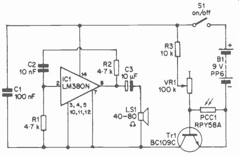
Fig.8--The circuit diagram of the Dark Alarm.
The breadboard component layout for the Light Alarm is shown in Fig. 7.
Incidentally, it is possible to alter the sound tone produced by the circuit; an increase in the value of R1, R2, or C2 (or more than one of these) produces a reduction in pitch, and vice versa.
=========
PARTS LIST FOR LIGHT ALARM
Semiconductors
IC1-LM380N, audio power amplifier
PCC1-Photo cell, type RPY58A or common silicon photo cells found in the hobbyist marketplace
Tr1-BC109C, ECG123A or 2N930, silicon NPN transistor
Resistors
R1, R2-4,700-ohm
R3, R4-10,000-ohm
Capacitors
C1--.1-µF, metallized polyester
C2-10-nF, metallized polyester
C3-10-µF, 25-WVDC, electrolytic
Additional Parts & Materials
B1-9-volt transistor-radio battery and connector to match
S1-S.p.s.t. miniature toggle
LS1-Loudspeaker, miniature, impedance in the range 40 to 80 ohms
Vero bloc or similar solderless breadboard or mating/matching printed-circuit board, solder, wire, etc.
===========
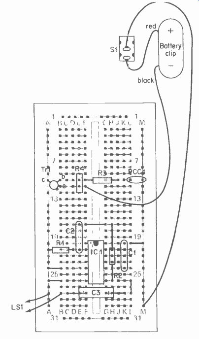
Fig. 7- Construction details of the Lig-it alarm.
Dark Alarm. With a minor circuit change (compare Fig. 6 with Fig. 8) the Dark Alarm circuit is similar to the Light Alarm just described, but it operates an audible alarm if the light intensity received by the photocell falls below a certain threshold level, rather than if it exceeds the threshold level. A possible application for the unit is as a headlights-on reminder for the driver of a car. The circuit will operate properly from a 12-volt car battery instead of a 9-volt transistor-radio battery provided nose filtering is provided in the battery line.
Control VR1 is used to set the light threshold.
6. SIG-TRACER
The purpose of a Sig-Tracer is much the same as that of a signal injector. However, a signal tracer is, in a way, used in the opposite manner to a signal injector. Instead of injecting a signal at the output of the equipment under investigation and then working towards the input, a signal tracer is used to first verify that an input signal is present, and further tests are then made at strategic points working stage-by-stage towards the output of the equipment. When the signal can no longer be traced (or is obviously at too low a level, seriously distorted, or in some other way incorrect) the approximate area of the fault has been located.
Normal voltage testing and similar checks are then used to precisely locate the fault.
A signal tracer for use on audio equipment simply consists of an audio amplifier driving a loudspeaker or an earphone, so that the traced signal, if present and correct, will give the appropriate audio output from the signal tracer. For RF or IF signal tracing the signal tracer must additionally have a suitable demodulator built-in so that an audio signal is produced from the tracer, provided a suitable input signal is present, of course.
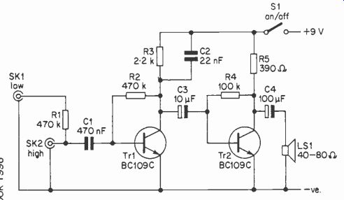
Fig. 9--The circuit diagram for Sig-Tracer.
The Sig-Tracer has good sensitivity so that it can be used for any normal type of audio signal tracing. The circuit provides AM demodulation, and the Sig-Tracer can therefore be used for IF and RF testing on AM radios provided a suitably strong antenna signal is available. The unit has an integral loudspeaker, and although the maximum output power is only a few tens of milliwatts, the volume level obtained is more than adequate for this application. If preferred though, the loud speaker could be replaced by an earpiece or head phones. Low, medium and high impedance headphones are all suitable for use with the unit.
The Circuit. The circuit diagram for the Sig-Tracer (see Fig. 9) is basically just two common-emitter amplifiers with capacitive coupling.
Transistor Tr1 is the input stage, and has C1 to provide DC blocking at the input, R2 as the bias resistor, and R3 as the collector-load resistor. An input signal from jack SK2 direct to the input of the amplifier (Tr1) may well be sufficient to overload the amplifier in many cases, and a second input having lower sensitivity is therefore provided (SK1), and the necessary attenuation (of nearly 40 dB) is provided by R1 and the input impedance of the amplifier. The input impedance of the amplifier at the high-sensitivity input
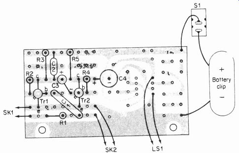
Fig. 10-The components layout for Sig-Tracer.
(SK2) is several thousand ohms, but R1 provides a useful boost in input impedance so that the input impedance at SK1 is approaching 500,000 ohms.
Capacitor C2 is used to roll-off the high-frequency response of the circuit in order to aid stability. It also gives the circuit a simple AM demodulator action by providing RF filtering.
The rectification that is also needed in order to produce AM demodulation is provided by transistor Tr1 which, like any amplifier, does not give perfect linearity. It tends to amplify more during positive input half cycles when the collector current increases than it does on negative input half cycles when the collector current decreases. This form of non-linearity is typical of any normal bipolar transistor, and gives the required rectification. There is no need to have any AF/RF switching since the circuit will properly process either type of signal.
=========
PARTS LIST FOR SIG-TRACER
Semiconductors
Tr1, Tr2--BC109C, ECG123A or 2N930, silicon NPN transistor
Resistors
R1, R2-470,000-ohm
R3-2,200-ohm
R4-100,000-ohm
R5-390-ohm
Capacitors
C1-0.470-µF, metallized polyester
C2-0.022-µF, metallized polyeste
C3-10--µF, 25-WVDC, electrolytic
C4-100--uF, 10-VVVDC, electrolytic
Additional Parts & Materials
S1--Miniature s.p.s.t., toggle switch
Aluminum case, printed-circuit board, perf-board or solderless bread board, miniature loudspeaker having an impedance in the range 40 to 80 ohms (LS1), two 3.5-mm jacks (SK1 and SK2) 9-volt transistor-radio battery and battery clip connector, test leads, wire, solder, etc.
=========
The output from the collector of Tr1 is coupled to the input of Tr2 by C3. Tr2 is used as a straightforward common emitter stage, but it is run at a fairly high collector current of around 15 mA so that a strong enough output signal to give reasonable volume from a high-impedance loud speaker can be obtained. C4 couples the output signal to the loudspeaker.
Construction. Before you begin, remember that it is advisable to fit this project into a metal case grounded to the negative terminal of the power sup ply so that the circuit is screened from stray electrical signals. A suggested component layout on a printed-circuit board for the project is shown in Fig. 10. The project is simple enough to do without a printed-
circuit board and may be assembled on a perf-board or some convention al pre-etched, general purpose, circuit board. As the input and output of the unit are in-phase, keep the speaker leads reasonably well separated from the input leads in order to minimize stray feedback and give good stability. It should not be necessary to use shielded leads to connect the board to jacks SK1 and SK2 in order to reduce feedback oscillations, but the external lead which connects to these sockets should be a shielded type.
The current consumption of the Sig-Tracer is about 17 mA, and, a standard 9V transistor-radio battery will not last very long on continuous ser vice. This will not matter in many cases since the unit is likely to be used intermittently during troubleshooting procedures. However, if it is envisaged that the unit will be used quite frequently and for long periods it would be wiser to use a larger battery.
7. CW Filter
Although the IF filtering of shortwave receivers has tended to improve somewhat over recent years, few receivers have a very narrow band width available, and this results in more adjacent-channel interference during CW (Morse code) reception than is really necessary. You have heard this interference: voice, music or hetero dyne signals (even excessive static) riding over code. A simple way of obtaining improved results with a receiver that does not have a built in CW filter is to use an add-on audio filter having a narrow bandwidth. If the receiver has a good filter for SSB reception, using an audio filter plus the SSB filter during CW reception should provide excellent results. We have just the unit for you: our CW Filter.
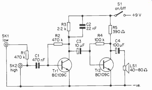
Fig. 11--Circuit diagram for the CW Filter.
The CW filter is connected between the head phone or loudspeaker socket or terminal strip of your receiver, and either the headphones or an external loudspeaker. The output of the receiver should have an impedance of 8 ohms or more. As the circuit provides unity gain at pass frequencies and a low impedance output, there should be no problems with a mismatching when the filter is in use.
The frequency response of the circuit peaks at approximately 800 Hertz, and the-6-dB band width is about 300 Hertz or so. The-0 dB points occur at about 350 Hertz and 2 kHz. This is sufficient to normally give a substantial reduction in adjacent channel interference, but the response is not so narrow and peaky that using the receiver with the filter in circuit becomes difficult, with the wanted signal tending to drift out of the pass-band and become lost.
The Circuit. Resistors R1 and R2 (see Fig. 11) form a simple attenuator which is needed to counteract the gain of the circuitry that follows, and thus give unity voltage gain overall. The rest of the circuit is a conventional operational amplifier bandpass filter having the circuit values chosen for the desired center frequency and a high Q value (to give the required fairly sharp, peaky response).
An ordinary operational amplifier would not give good results in this circuit due to the limited current drive capability of typically just a few milliamps. A few high-current operational amplifiers are available, but even these can usually only provide a few tens of milliamps, and cannot provide a very high output power. This circuit is based on a TDA2006 device which is primarily intended for use as an audio power amplifier having an output power of up to about 10 watts, and the output overload protection circuitry within the device limits the output current to about 3 amps!
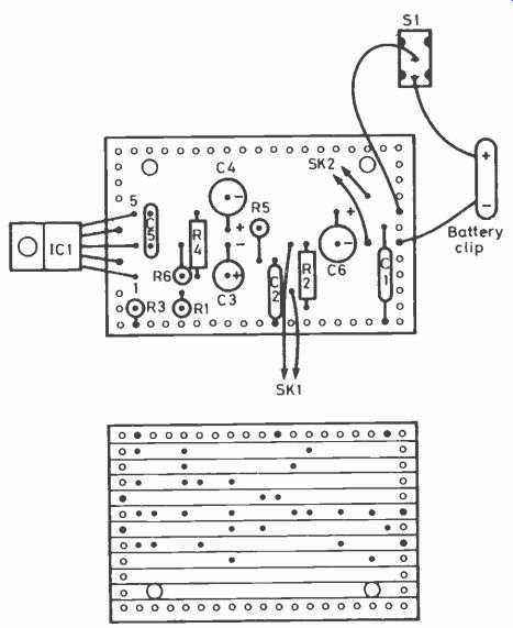
Fig. 12-- Suggested parts layout on a stripboard for the CW Filter. Details are provided in text.
==========
PARTS LIST FOR CW FILTER
Semiconductor
IC1-TDA2006, power amplifier
Resistors
R1, R3-2,700-ohm R2-100 –ohm
R4, R6--33,000–ohm
R5-180,000–ohm
Capacitors
C1, C2-10-nF, metallized polyester
C3--10-µF, 25-WVDC, electrolytic
C4-C6-100-µF, 10-WVDC, electrolytic
Additional Parts & Materials:
S1-S.p.s.t. miniature, toggle-type switch
Suitable aluminum case, perfboard or 0.1-in matrix strip-board, 2 RCA phono jacks (SKI and SK2), DC power
supply (see text), wire, solder, etc.
===========
Although intended for use as an audio power amplifier, the TDA2006 is a very adaptable device because it can really be regarded as an operational amplifier having a high-power, class B, output stage. The TDA2006 has inverting and non-inverting inputs with a high-input impedance (5 Megohms) at each of these, plus a high open-loop voltage gain over the audio frequency range. Unlike many audio ICs which are basically operational amplifiers, the TDA2006 does not have any internal biasing components, and it can therefore be used, as it is here, in standard operational amplifier circuit configurations.
The lowest recommended supply voltage for the TDA2006 is 12 volts, but it seems to operate well using a 9-volt battery as the power source.
The current consumption is around 20 mA or so, and this can rise substantially if the circuit is used at high volume with an 8 ohm load. It is therefore advisable to use a fairly large battery pack or suit able 12-volt DC wall plug power pack. A supply voltage of 12 or 15 volts is perfectly acceptable provided C6 working DC voltage (WVDC) has a suitable high, maximum-voltage rating.
Construction. The component layout and wiring of the CW Filter are illustrated in Fig. 12.
Construction of the component panel is very straightforward, and there are no breaks needed in the copper strips. IC1 has pre-formed leads and it is necessary to splay the readouts slightly in order to fit them onto a 0.1-in. matrix. IC1 should not need a heat sink if the circuit is battery powered, but this might be necessary if a 12 or 15 volt high-current battery supply or AC-line power supply is used.
If an operating frequency other than 800 Hertz is desired, the center frequency of the filter can be changed by altering the values of C1 and C2.
The operating frequency is inversely proportion al to the value of these capacitors, but note that reducing the center frequency also reduces the bandwidth of the filter, and increasing the center frequency gives an increase in bandwidth.
When first using the filter it may appear to give a large reduction in gain, and this is simply due to the fact that at most frequencies the filter does give a substantial amount of attenuation.
The CW note from the receiver must be fairly accurately tuned to the center of the filter's response in order to obtain a strong output, and after a little experience with the unit, this tuning will be found to be quite easy.
---------------------
8. Vol-Expander
Many types of live music, particularly classical music, have a very wide dynamic range. The dynamic range of music is simply the difference between the maximum and minimum sound levels, usually expressed in dBs. This dynamic range can be over 70 dB (although in most cases it is not quite this high).
To record this type of music requires a certain amount of compression being used in one form or another, especially in the case of a cassette recording where the available dynamic range of the recording system (tape and machine) is likely to be limited. Without some form of compression to restrict the dynamic range of the signal either loud passages of music overload the recording or transmission medium, of quiet passages fall into or below the noise level (or a combination of tie two).
Music that has undergone even a small amount of carefully applied compression can be rather lacking in musical impact. You hear that kind of flat, background music in elevators and banks. An improvement in the playback can often be obtained by using a certain amount of expansion during playback or reception in order to boost the effective dynamic range of the signal. In order to give the desired effect an expander is required not to a Elect low-level signals, but produces a small boost in volume at middle dynamic levels, steadily rising to an increase of about 10 or 12 dB at the highest dynamic levels. In this way the lowest volume levels (and the back ground noise) remain unaltered, but the highest volume levels are substantially boosted. Of course, some noise is also boosted, but this is not noticeable as the wanted signal is strong enough to mask the noise.
Thus the use of a volume expander gives an apparent increase in signal to noise ratio, and can give more impact to music which requires a wide dynamic range. A volume expander cannot be expected to precisely counteract any compression used during the recording process or during transmission, but it can nevertheless produce a substantial subjective improvement when used with many program sources.
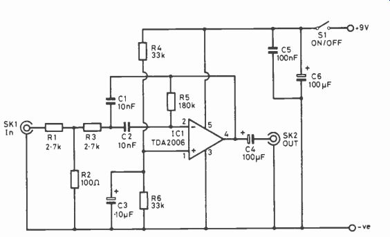
Fig. 13--Circuit diagram for Vol-Expander.
This all leads to the Vol-Expander that is our budget version of a practical volume expander hobbyists can build and use with rewarding music enjoyment.
The Circuit. An operational transconductance amplifier makes a good basis for our Vol-Expander since it is essential that the expansion is applied gradually, and is not virtually switched on and off. A voltage-controlled amplifier (VCA) using an operational transconductance amplifier tends to naturally give a suitable control characteristic. The circuit diagram of the Volume Expander is shown in Figure 13, and the operational transconductance amplifier used in the unit is a LM13600N device (IC1). This device has a number of additional features when compared to a basic device such as the CA3080E, the most obvious one being the fact that it is a dual device, and only one section of the device is used.
it diagram for Vol-Expander.
The other additional features of the LM13600N are the inclusion of a Darlington pair-emitter follower stage for use at the output of each section of the device, and linear diodes at the input of each section. The linear diodes can be fed with a small bias current, and this enables the device to handle a significantly higher signal level (about 10 dB in fact) before serious distortion occurs. This enables a higher overload mar gin and (or) increased signal-to-noise ratio to be achieved.
Resistor R8 is the discrete load resistor for the internal buffer stage of IC1, and R6 provides the bias current for the linear diodes. R7 sets the quiescent voltage gain of the circuit at a little under unity.
Some of the input signal is coupled by C4 to the input of a common-emitter amplifier which utilizes Tr1. The amplified output from Tr1 is coupled by C5 to a rectifier and smoothing circuit which produces a positive bias voltage which is roughly proportional to the input signal level.
This signal is applied to the amplifier bias input of IC1 via R12.
If only a low input-signal level is present there will be little or no current flow through R12 and into the amplifier bias input of IC1, and the voltage gain through the circuit will not be significantly changed. At higher signal levels the bias potential produced across C6 becomes large enough to produce a significant current flow
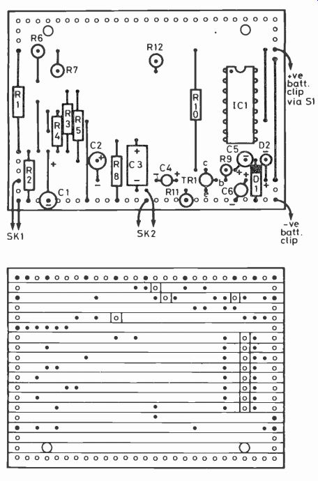
Fig. 14-Construction details of the Vol-Expander.
through R12, and the gain of the circuit is boosted somewhat. At high signal levels of around 500 mV rms, the bias voltage becomes high enough to produce a boost in gain of around 12 dB. This is about the maximum expansion that can be used without the signal processing becoming obvious.
Capacitor C6 has been given a fairly low value so that the attack and decay times of the circuit are both fairly short, and the unit responds very rapidly to changes in the input level. However, the attack and decay times are made sufficiently long to prevent significant distortion from being produced.
=========
PARTS LIST FOR VOL-EXPANDER
Semiconductors
IC1-LM13600N, transconductance linear opamp
Tr1-BC109C, ECG123A or 2N930, silicon NPN transistor
D1-D2-1N4148, silicon signal diode
Resistors (1/2- or 1/4-watt, 5%; 10% over 1 Megohm)
R1, R2-3,900-ohm R3-220-ohm R4-15,000-ohm R5-10,000-ohm R6-68,000-ohm R7-39,000-ohm R8-3,300-ohm R9-1.8 Megohm R10-4,700-ohm R11-120-ohm R12-10,000–ohm
Capacitors
C1-100-µF, 10-WVDC, electrolytic C2-4.7-µ,F, 1 0-VVVDC, electrolytic C3-10-µF, 25-WVDC, electrolytic C4-220-µF, 35-WVDC, tantalum C5-1-µF, 10-WVDC, electrolytic C6-330-µF, 35-WVDC, tantalum
Additional Parts & Materials
S1, S.p.s.t. miniature, toggle switch
Suitable aluminum cabinet or box, 0.1-in matrix strip-board or pert-board, two RCA phono jacks (SK1 and SK2), 9-volt transistor-radio and battery-clip connector, wire, solder, etc.
=========
The current consumption of the circuit is only about 6 mA, and a small 9-volt transistor-radio battery makes an economic power source.
Construction. An 0.1-in. matrix stripboard panel for the Vol-Expander is detailed in Fig. 14, and a board having 19 copper strips by 27 holes is required. If you cannot obtain this board, a perf-board of the same size with flea clips inserted may be used. Interconnect the flea clips with No. 22 copper wire. Jacks SK1 and SK2 are the popular audio RCA phono types on the prototype.
If a stereo expander is required, it will be necessary to make up two boards, one to process each stereo channel. Alternatively, a longer piece of stripboard or perf-board could be used, and the otherwise unused section of IC1 could then be used as the basis of the additional expander circuit. The power supply center tap provided by RI, R2 and C 1 could be used for the additional expander circuit, but all other components (apart from IC1 of course) would need to be duplicated in the extra expander circuit.
The Vol-Expander circuit should give good results if fed with the output of a tuner, cassette or tape deck, or a record deck via a suitable preamplifier. Some items of equipment might be found to have too little output to drive the circuit properly, and it will then be necessary to reduce the value of R11, or to even replace it with a shorting link. It is just possible that some signal sources will provide too strong a signal so that the expansion commences at a fairly low level, and in such cases R11 can be increased in value.
If preferred, R11 could be replaced by a 1000-ohm linear potentiometer which would be adjusted for (subjectively)the best results.
--------------
9. COMPUTER VOICE
Need a mechanical-sounding voice, often called a "computer voice"? Well, here's a simple circuit that can be put to good use in amateur dramatic productions, telephone message tapes, etc. It's easy to produce synthetic- or computer-type voice effects from an ordinary voice-signal input.
There are several ways to generate this effect, but probably the simplest method that gives good results is to amplitude modulate the ordinary voice signal by using a squarewave as the modulating signal. This is similar to the well-known tremolo effect which is sometimes used with guitars and other electronic instruments, but tremolo units normally use a triangular or sinewave modulation signal to give a smoother form of modulation. In this application a squarewave gives better results, and a sinewave or triangular wave form would be loss effective. The unit switches the input signal between being passed straight through to the output, and being attenuated by around 20 dB, or so. A switching rate of a few Hertz is used.
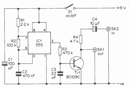
Fig. 15-The circuit diagram for the Computer Voice unit.
========
PARTS LIST FOR COMPUTER VOICE
Semiconductors
IC1-555 timer chip
Tr1-BC109C, ECG123A or 2N930, silicon NPN transistor
Resistors
R1-2,200-ohm R2-100,000 –ohm
R3-470,000-ohm R4-4,700 –ohm
Capacitors
C1-100-µF, 10-WVDC electrolytic C2-0.47-uF, metallized polyester C3-22-nF, metallized polyester C4-10-µF, 25-WVDC electrolytic
Additional Parts & Materials
S1--S.p.d.t. miniature toggle
Aluminum case, solderless or perf-board circuit board, 9-volt transistor-radio battery and matching battery clip, two 3.5-mm jack sockets (SK1 and SK2) or reasonable substitute, wire, solder, etc.
========
The Circuit. The circuit diagram of the Computer Voice unit is given in Fig. 15. It consists of two sections: an oscillator to provide the modulation signal, and the modulator itself.
The oscillator uses a 555 timer chip in the astable multivibrator mode, and the frequency of operation has been set at about 10 Hertz by the values given to R1, R2 and C1. The mark space ratio (duty cycle) is virtually one to one as the value of R2 has been made high in value relative to the value of R1.
A very simple modulator is used, but this is quite all right in this application where a small amount of distortion is quite acceptable.
Distortion produces new frequencies that help to change the voice signal and make it sound less like the original. A large amount of distortion is obviously not desirable as it would severely impair the intelligibility of the output signal.
Transistor Tr1 is used as a sort of voltage con trolled resistor: and, in conjunction with R4, it forms a voltage controlled attenuator. Capacitor C4 is merely a DC blocking capacitor at the input and R3 is used in the base circuit of Tr 1 to effectively make Tr 1 a voltage-controlled device rather than a current-controlled one. During the periods when IC1 's output is high, Tr1 is biased into conduction by the base current it receives via R3, and effectively has a collector-to-emitter resistance of only a few hundred ohms. This gives losses of around 20 dB or so through R4, and attenuates the signal fed to the output by this amount. When IC1's output is low, Tr 1 is switched off and the input signal can pass straight through R4 to the output. The only attenuation is due to the potential divider action between R4 and the input impedance of the equipment to which the output signal is fed. This should minimize losses.
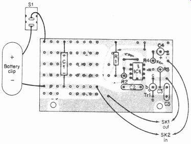
Fig. 16--The Computer Voice unit assembled on a multi-project board: The text
advises using a solderless circuit board. Use that which is most comfortable
for you.
Thus the output signal is switched up and down in amplitude, producing the required computer-type voice effect. Capacitor C3 is included in the circuit to slightly slow down the sharpness with which the signal is switched between the two levels of gain, and this helps to avoid "clicks" which can otherwise occur during transitions from one gain level to the other. Capacitor C1 is a power-supply decoupling capacitor and this also helps to prevent switching "clicks" from being generated within the unit.
Construction. It is advisable to assemble the project on a solderless circuit board as illustrated in Fig. 16. Assembly is easy and experimental changes in component values will enable you to customize the output voice signals to your taste.
Jack sockets (3.5-mm) were used for SK 1 and SK2 on the prototype but these can be any two way audio connectors. It is a good idea to house this project in an aluminum metal case (grounded to the negative supply rail of the circuit) so that the circuitry is screened from power-line hum, radio frequency signals, and other possible sources of electrical interference.
The unit can be used to process a signal directly from a microphone, but this may well cause problems with large losses through the unit even when Tr1 is in the off state. This loss is due to the fact that some microphones are designed to feed into quite a low impedance, and with such a load-impedance mismatch substantial losses occur.
Some microphones are designed to feed into high impedance and will not produce this problem.
Nevertheless, as microphones of this type have quite a high impedance, the losses provided by the unit when Tr1 is in the on state will be much higher than is really desirable. There is also the problem of the low-output level of a microphone that requires a high level of gain from the unit.
This amplification will also boost the noise level to an uncomfortable listening level.
It is better to feed the microphone signal to the unit via a preamplifier, so that a fairly high-signal level is fed to the unit. A mere one stage of isolation with attending load matching is invaluable here.
There should be no problems if the unit is fed from a tape recorder or some piece of equipment which provides a similar signal level (a few hundred millivolts rms). It is not advisable to use the unit to process a signal having an amplitude of more than about 1.0 volt rms as quite severe distortion could then be produced.
---------------------
10. Audio Power Booster
Despite the fact that there is a fair amount of noise inside most cars when they are traveling, many car radios and tape players have rather insufficient output powers to play over road noise. One reason for this is probably the fact that it is not possible to obtain a great deal of power using a 12-volt DC supply and a modern transformerless output stage into a 4- or 8-ohm loud speaker. The maximum possible output swing is nominally 12 volts peak-to-peak. No output stage gives an output voltage swing equal to the supply voltage as there are inevitably voltage drops through the output transistors. On the other hand these are counteracted to some extent by the fact that a car battery usually has an actual voltage which is somewhat more than its nominal level.
In terms of rms voltage this limits the maximum output to only about 4.25 volts, which gives only about 2.25-watts rms into an 8-ohm speaker, or 4.5-watts rms into a 4-ohm type.
There are ways of obtaining increased output, and the method used in the Audio Power Booster is to use a bridge-amplifier circuit. The Audio Power Booster is connected between the car radio or tape player and the loudspeaker, and it gives an output power boost of about 9-watts rms into an 8-ohm load or 18-watts rms into a 4-ohm load.
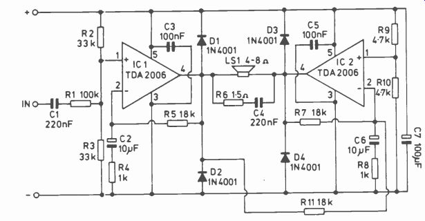
Fig. 17--The circuit diagram of the Audio Power Booster. Notice the almost
mirror image of the circuit components surrounding the ICs.
A Bridge Does It. A bridge-amplifier circuit consists of two power amplifiers with the loud speaker being driven from the two outputs; neither speaker lead being connected to the car's chassis ground. The two amplifiers are arranged so that under quiescent conditions their outputs are at the usual level of about half the supply voltage, and there is no significant voltage pre sent across the loudspeaker. The amplifiers are arranged to have output signals that are in anti phase, so that a positive change in the output potential of one is matched by a similar but negative change in the output voltage of the other.
Thus when one amplifier has its output fully positive, the output of the other one is fully negative.
This gives about 12 volts across the loudspeaker.
On signal peaks of the opposite polarity the two output states are reversed so that 12 volts is again developed across the loudspeaker, but the polarity of the output signal has changed. Thus the amplifier can give up to ±12 volts across the loudspeaker, or E peak-to-peak voltage swing of 24 volts. This is double that obtained with a normal amplifier, and gives a maximum output current that is also doubled; thus the output power for a given speaker impedance is boosted by a factor of four when compared to an ordinary audio power amplifier.
The Circuit. The Audio Power Booster is based on two TDA2006 audio IC power amplifiers, as can be seen from the circuit diagram of Fig. 17.
Power amplifier IC1 is used as what is virtually a non-inverting amplifier, with the non-inverting input of the device being biased to half the supply voltage by R2 and R3. R5 provides 100-percent negative feedback from the output to the inverting input of IC1 at DC so that the circuit has unity voltage gain and the output is biased to the required level of half the supply voltage. C2 and R4 remove some of the feedback at audio frequencies and :his gives a voltage gain of about 18 times at these frequencies. This is far more than is actually needed, and a voltage gain of little more than unity is in fact sufficient. It is necessary to remove a substantial amount of feedback though as instability is otherwise likely to occur. R1 is used at the input of the amplifier to reduce the sensitivity to a more suitable level, and C1 simply provides DC blocking at the input.
IC2 is used n virtually the same configuration, but its non-inverting input is not fed with an audio signal, and only receives the DC bias signal from R9 and R10. Resistors R2, R3, R9 and R10 are all close tolerance components so as to ensure a reasonably small voltage difference across the outputs of the two amplifier stages under quiescent conditions; and, consequently, a small and insignificant quiescent current through the loudspeaker.
Resistor R11 couples the output signal of IC1 to the inverting input of IC2, and the value of R11 is chosen to give IC2 an effective voltage gain of unity. However, as the input signal is coupled to IC2's inverting input there is a phase inversion through this section of the amplifier, giving the required anti-phase relationship at the two outputs.
Diodes D1 to D4 are protection diodes for the two ICs, while R6 plus C4 form a Zobel network which helps to prevent instability. Components C3, C5 and C7 are all supply decoupling capacitors.
----------
PARTS LIST FOR AUDIO POWER BOOSTER
Semiconductors
IC1, IC2-TDA2006 audio power amplifier chip
D1-D4--1N4001 rectifier
Resistors:
R1--100,000-ohm R2, R3-33,000-ohm, 2%
R4, R7-100-ohm
R5, R11-18,000 –ohm
R6-1.5-ohm
R8-1,000–ohm
R9, R10-4,700-ohm, 2%
Capacitors:
C1 Mylar
C2, C6-10-uF, 25-WVDC, electrolytic
C3,C5-.1-µF, metallized polyester
C7-100-uF, 25-WVDC, electrolytic
Additional Parts & Materials
Suitable aluminum chassis box, 0.1-in matrix stripboard or pert-board, transistor heat sinks (see text), s.p.s.t. switch (optional), sockets, wire, solder, etc.
-----------
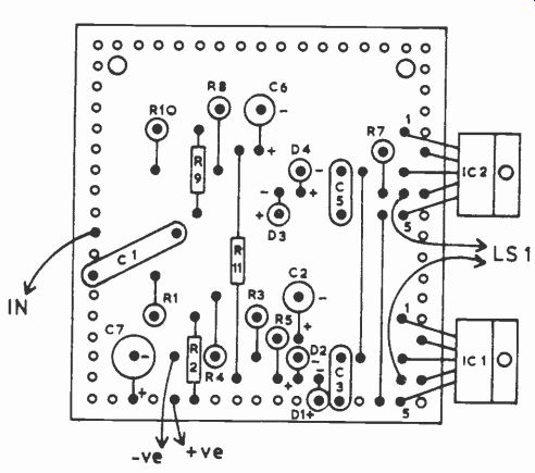
Fig. 18--Component layout for the Audio Power Booster as placed on a 0.1-in.
matrix stripboard. The copper strips (on the reverse side of the board) run
horizontally from left to right. If perfboard is used, interconnect all leads
on the common horizontal row of holes for each strip.
Construction. A 0.1-in. matrix stripboard having 18 copper strips by 17 holes is used to accommodate most of the components, and the component layout of this board is given in Fig. 18. There are no breaks in any of the copper strips. The audio power ICs are modern types which physically resemble plastic power transistors, but they have five rather than three leads.
These must be carefully bent apart slightly in order to fit these devices into this stripboard.
Ensure that you do not omit the two jumper (link) wires. Be very careful to connect the polarized components with the correct polarity, especially the four rectifiers as these could be damaged or cause damage if connected incorrectly. Use the same care with electrolytic capacitors.
The two ICs should be bolted to a substantial heatsink. If the unit is used in a negative ground vehicle it can be fitted into a metal case which can be used as the heatsink, but it will probably be necessary to use an aluminum bracket to provide a thermal path from the ICs to the case. A suitable bracket can easily be produced from #18 swg aluminum that is commonly used in manufactured chassis boxes.
In positive ground cars this is not really advisable since the heat-tabs of the ICs connect internally to their negative supply readouts. This would result in the case connecting to the negative supply, and the likelihood of a short circuit between the case of the booster and the positive chassis of the car. Insulation sets supplied with the semiconductors can be used to insulate the heat-tabs from the case. Do a careful job since vibrations may shake the parts apart Components R6 and C4 are not mounted on the component panel, but are wired across the output socket or terminals of the Audio Power Booster.
When installing the booster remember that neither output lead should be allowed to come into contact with the chassis of the vehicle. The TDA2006 incorporates output short-circuit protection circuitry and thermal overload shutdown circuitry, and accidental contacts between the output leads and the chassis (or each other) should not damage the unit.
Power. The power supply voltage for the unit should be taken from the supply line of the radio or tape player with which the booster is employed, as it will then be switched on and off with the main item of equipment. However, the unit can have its own on/off switch added into whichever supply lead is not grounded. The input for the booster is taken from whichever output lead of the radio or tape player is not grounded, and the correct lead can be found simply by connecting the two leads, in turn, to the input of the unit to see which one provides the desired result.
If the unit is used with a radio or tape player that has only a very limited output power it may be necessary to reduce R1 in value somewhat in order to fully drive the booster.
------------------
(cont. to part 2)