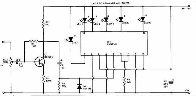
LED VU Meter
This simple peak reading VU meter circuit uses six LEDs to indicate six signal levels at - 14, - 8, - 3, 0, +3, and +6dB, or any other levels having the same spacing (e.g. - 17, - 11, - 6, - 3, 0, and +3dB, if preferred). About 24mV peak to peak is needed in order to activate the highest LED indicator, so the circuit is sufficiently sensitive to be used with any normal item of audio equipment.
The circuit is based on an LM3914N bargraph display driver device (IC1), which can be used to drive up to ten LEDs. This is connected so that with OV12 at the input only the first LED indicator switches on. With the input raised to OV24 the second LED switches on as well; OV36 causes three LEDs to switch on and so on up to an input of 1V2 or more whereupon all ten LEDs are activated. In this circuit only LEDs 1, 2, 3, 5, 7 and 10 are included in the display, and these are D1 to D6 respectively.
The input signal is taken to a variable attenuator which enables the sensitivity of the circuit to be set at the correct level. The signal is then passed to a low gain common emitter amplifier based on Q1 which gives a tenfold boost in the sensitivity of the circuit. C2 couples the output from Q1 to the input of IC1. R5 is the input bias resistor for IC1, and D7 protects IC1 against an excess negative in put voltage. R6 sets the current to each LED at about 12mA, but as IC1 responds only to positive half cycles the LEDs can switch on for a maximum of 50% of time. This gives an effective LED current of 6mA. The quiescent current consumption of the unit is about 8mA, rising to an absolute maximum of 44mA with all six LEDs activated.
To calibrate the unit, a 0dB test signal should be fed into the equipment and R1 adjusted for the lowest sensitivity that does not cause the 0dB LED to extinguish.
The input impedance of the unit is about 80k and it will only lightly load the monitored equipment.
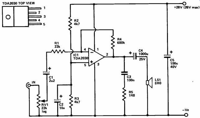
General Purpose Amplifier
This useful amplifier will provide an output power of up to about 8 watts rms at low distortion (less than 0.1% THD) into an 8 ohm loudspeaker when using a 28 volt supply. If used with a 4 ohm loud speaker the output power is increased to about 12 watts rms or so, with the distortion being roughly doubled (although obviously still quite low). The circuit will operate with lower supply voltages, down to less than 9 volts, with a reduction in the maximum output power.
The circuit utilizes a TDA2030 integrated circuit, a modern device superior in performance and easier to use than most previous devices.
It is used in much the same way as an operational amplifier and like an operational amp it has both inverting (-) non-inverting (+) inputs. In this circuit it is used in the inverting amplifier mode.
The non -inverting input is biased to half the supply potential Audio by R2 and R3; C2 decouples any hum or other noise from the supply lines. R4 biases the inverting input of IC1, with a negative feedback action stabilizing the output at half the supply voltage under quiescent conditions. This ensures that the circuit can provide the highest possible un clipped peak to peak output voltage swing (and output power).
R4 also forms part of the network which sets the gain and input impedance of the circuit, with R1 forming the other half. The voltage gain is approximately equal to R4 divided by R1, about 30 with the specified values. This gives the circuit an input sensitivity of about 260mV rms for 8 watts into 8 ohms. The value of R1 sets the input impedance of the amplifier at 22k, but volume control VR1 shunts the input to give a minimum input impedance of 11kR.
Input and output DC blocking are given by C1 and C4 respectively. C3 and R5 are a Zobel net work and aid the stability of the circuit. C5 provides supply de-coupling and should be mounted close to IC1.
++++++++++++++++++++++++
Clipping Monitor
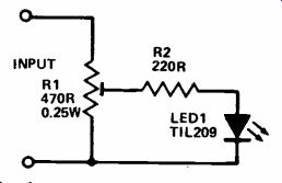
WHEN using an amplifier at virtually its full output power there is a risk of "clipping" occurring. The amplifier is overdriven to the point where output peaks are flattened because the amplifier simply can not provide a high enough output voltage. The distortion caused by clipping is often quite severe and readily apparent, but this is not always the case. It is not uncommon for the tweeters in loud speakers to burn out due to overloading caused by clipping producing strong high frequency signals!
The circuit relies on the fact that with less than about 2V applied to a LED it will not pass any significant current and will fail to light up. If the voltage applied to the LED is only marginally increased above 2V, the LED avalanches, a heavy current flows and it glows brightly. R1 is adjusted so that the voltage applied to LED1 via current limiting resistor R2 is just sufficient to cause D1 to low quite brightly when the amplifier is driven into clipping. With the amplifier driven just below the clipping threshold there is just enough voltage applied to the circuit to cause LED1 to visibly glow, al though it does so at less than full brightness. If the amplifier is driven significantly below the clip ping level there will be insufficient voltage fed to D1 to cause it to conduct and it will not light up.
+++++++++++++++++++
Power Amplifier
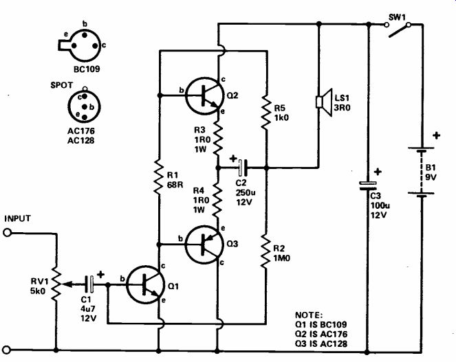
Most Hi Fi amplifiers are similar to this design. The circuit uses a complementary output stage with one NPN and one PNP power transistor; this eliminates the need for an output transformer. Output power is close to 1W with reasonably low distortion.
The input signal is passed through the volume control RV1 and then via C1 to the base of Q1.
The collector load for Q1 is composed of R1, R5 and the loud speaker and the voltage at the collector will be about half the supply voltage, i.e. 4V5. The bases of Q2 and Q3 are also at the same voltage (very nearly) as the collector of Q1 because the value of R1 is so low.
At the junction of the emitters of Q2 and Q3 the voltage will also be very nearly 4V5. R3 and R4 limit the current through Q2 and Q3.
When the amplified input signal is less than 4V5, Q2 is turned off but Q3 will conduct. When Q1 amplifies the signal to above 4V5 the reverse happens; Q2 conducts and Q3 is turned off.
The signals are combined at the common emitter junction of Q2 and Q3 and passed to the loud speaker through the large electrolytic capacitor C2. Small values of C2 result in a poor low frequency response. Negative feedback is provided by R5 and R2; these en sure stability by reducing the gain slightly. R1 is included to provide a small amount of base bias for Q2 and Q3; more sophisticated de signs use thermistors or diodes to prevent thermal runaway.
A disadvantage is the DC coupling of the transistors; the output pair should be 'matched pair', other types can be tried as long as they are also 'matched pairs'.
++++++++++++++++
Cassette Radio Booster
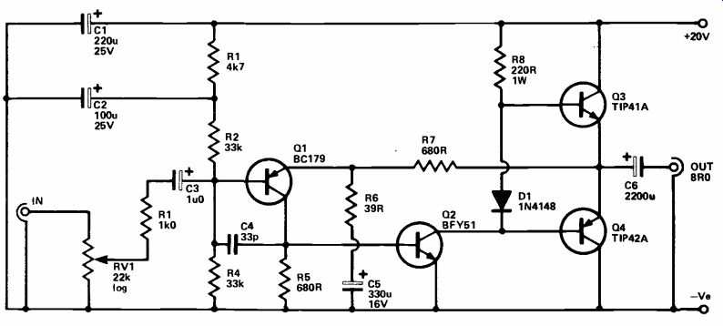
This amplifier was designed as a booster to enable output powers of around 4 to 5 watts rms to be obtained from a radio/cassette unit. Of course, the amplifier is also suitable for other applications; it has an output sensitivity of approximately 350mV rms into 10k for maximum output, and is intended to feed an 8 ohm load.
The circuit uses a well known configuration which has common emitter input stage (Q1) direct coupled to common emitter driver stage (Q2), which is in turn direct coupled to the complementary emitter follower output stage (Q3 - Q4). R7 provides virtually 100% negative feedback at DC, giving the circuit approximately unity voltage gain at DC. R1 R2 and R4 form a potential divider which bias the input of the amplifier to about half the supply potential and the output is also biased to about this level due to the DC unity gain. This bias level gives the optimum unclipped output voltage swing. R1, C1 and C2 filter out any hum or noise which might otherwise be coupled from the supply lines to the input via the bias circuit. R6 and C5 are used to decouple some of the feedback at audio frequencies, and thus give the unit a useful voltage gain at these frequencies.
D1 is used to give a small standing bias to the output transistors and, together with the fairly substantial amount of negative feedback, reduces cross -over distortion to an unnoticeable level.
The emitter follower output stage gives the circuit a low output impedance so that the load can be efficiently driven with high output currents. 03 drives the speaker during positive going output excursions while Q4 drives the speaker during negative output excursions. C6 provides DC blocking at the output, and C3 provides the same function at the in put and C4 aids the stability of the circuit. RV1 is a volume control, and results will probably be best if the volume control on the cassette radio is set for a fairly high output (but not so high as to cause clip ping), and the volume is adjusted using RV1.
The circuit requires a stabilized supply of 18 to 22 volts, and cap able of providing up to 400mA. Q2 should be fitted with a clip-on TO-5 size heatsink. Q3 and Q4 are both fitted with commercially made, finned, bolt -on heatsinks.
+++++++++++++++++++
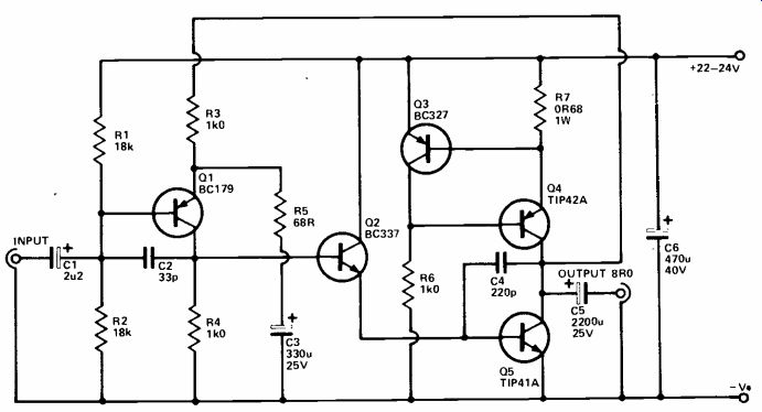
Class A Amplifier
This design gives an output power of about 4.1 watts rms into an 8 ohm load, but requires a supply of 22 to 24 volts at 1 amp. This gives an efficiency of about 19% at best, less than a third of the efficiency of many Class B designs.
Q1 is used in the common emitter input stage, and is direct coupled to the output stage via emitter follower buffer transistor, Q2.
The latter is needed because of the fairly high drive current required by the output stage. Q5 is the output transistor, employed in the common emitter mode. It has a constant current source as its collector load, formed by Q3, Q4, and R7. The latter sets the output current of the circuit at just under 1 amp. The constant current genera tor load gives better efficiency than a load resistor and also gives good linearity.
R3 gives virtually 100% negative feedback over the amplifier at DC, giving unity voltage gain. By biasing the input to half the supply voltage using R1 and R2, the output is also biased to the required level of half the supply voltage. R5 and C3 decouple some of the feedback at audio frequencies, giving the circuit a sensitivity of about 380 mV rms for maximum output.
C2 and C4 aid stability, while C1 and C5 provide DC blocking at the input and output respectively.
Q4 and Q5 must be mounted on a substantial heatsink.
++++++++++++++++
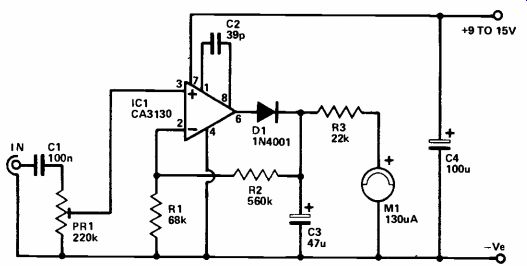
Peak Reading VU Meter
The type of VU meter normally employed in tape decks and other items of audio equipment is the average reading type. These can give misleading results on signals that have a pulse -like waveform of relatively low average amplitude for the peak amplitudes involved.
This can lead to overloading and consequent distortion on signals of this type, eg piano and percussion. One way around this problem is to use a peak reading VU meter. This has a fast attack and slow decay time so that it res ponds properly to brief and intermittent signals. The normal response times for a unit of this type are 2.5ms attack and 1s decay.
This unit roughly adheres to these figures.
IC1 is an operational amplifier which is used in the non -inverting mode. R1,2 form a negative feed back network which sets the closed loop voltage gain of the circuit at a little under ten. D1 is included at the output so that IC1 can supply an output current, but a current cannot flow into the output of IC1. The feedback is taken from the junction of D1, R2 etc., so that the input voltage appears here amplified by about ten times and the feedback overcomes the non -linearity of Dl. C3 is rapidly charged to the peak output voltage as it is fed from the fairly low impedance of IC1 and D1. Its only discharge paths are through the much higher impedances of R1 -R2 and R3 -M1. This gives the circuit the required fast attack and slow decay times. M1 responds to the voltage across C3, which is, of course, proportional to the peak positive input level (the circuit is a halfwave type and does not res pond to negative going inputs).
The VU meter movement used in the prototype had a FSD value of 130uA, but the circuit should work with any type having a sensitivity of between about 50 and 200uA.
R1 biases the non-inverting in put of IC1 to the negative rail and also enables the sensitivity of the circuit to be adjusted to the correct level. At maximum sensitivity, less than 1V peak to peak is needed for FSD of M1. Current consumption is only 400uA.
++++++++++++++++
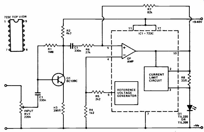
Peak Level Indicator
Peak audio level indicators can be used in tape recorders, amplifiers, mixers, and other radio equipment to provide a visual overload warning, and unlike slower res ponding VU meters, they produce a proper response to fast transients. The circuit is based on the inexpensive 723C device which, although primarily intended for use as a voltage regulator, can be adapted to work well in many other applications.
The 723C has a highly stable 7V (nominal) reference voltage avail able at pin 6. This is coupled to the inverting input of an operational amplifier (which is also part of the 723C device) via an attenuator, R4, 5. This gives a stable reference potential of a little over 2V at the inverting input. The input signal is coupled by way of sensitivity control RV1 to a common emitter amplifier based on Q1 and fed to the non -inverting input of the operational amplifier by C2 and R6. Under quiescent condition or with a negative going signal at Q1 collector, the non -inverting input will be at a lower potential than the inverting one, and the output of the amplifier will be low. If a positive going signal reaches a high enough amplitude, though, the non-inverting input will reach a higher potential than the inverting one causing the output to go high. D1 is then switched on with a current that is determined by the output of the amplifier and which is largely independent of the supply voltage. Discrete resistor R8 actually sets the output current.
The specified value gives a nominal 20mA LED current. R7 provides positive feedback which ensures that D1 is either fully on or off. It also tends to hold D1 in the on state for slightly longer than would otherwise be the case, thus giving a clearer indication of a brief overload.
The unit can be adjusted to res pond to input levels down to about 100mV rms, which should be more than adequate for all normal requirements. RV1 is adjusted for the lowest sensitivity that causes D1 to come on with an in put signal level equal to the lowest overload level. Quiescent current consumption is about 4mA.
++++++++++++++++
Active Tone Controls
This tone control circuit is easy to incorporate in a stereo amplifier, disco unit or whatever, as it has a high input impedance (over 100kR), a nominal voltage gain of unity and a low output impedance.
The usual bass and treble controls are included in the unit, with about 12 dB of boost and cut being avail able at 100Hz and 10kHz. The noise and distortion produced by the circuit are both extremely low due to the large amount of negative feedback used and the unit can handle output signal levels of several volts rms without clipping.
Q1 is used in a straightforward emitter follower buffer stage that gives the unit a high input impedance. C2 couples the output of Q1 into the tone control circuitry.
This is an active circuit which provides frequency-selective negative feedback over an amplifier. The amplifier uses Q2 as a conventional common emitter stage direct-coupled to emitter follower output transistor Q3. The latter gives the unit a low output impedance.
The tone control networks are slightly simpler than the usual Baxandall configuration, but give a perfectly acceptable level of performance. RV1 controls the bass while RV2 is the treble control.
Feedback is at a maximum with the sliders of the potentiometers to the right and at a minimum with the sliders set fully to the left. Of course the gain of the circuit is inversely proportional to the level of feedback. Maximum feedback therefore corresponds to maximum cut and not to full boost. The current consumption of the circuit is a little under 1mA per supply.
+++++++++++++++++
Peak Limiter
The circuit is designed to take almost any audio input but the output will have all peaks above a certain level, which can be adjusted, eliminated.
The circuit can either be wired into a receiver circuit or directly from a headphone socket. If wired into circuit permanently, RV1 should take the place of the normal volume control and the output should be wired to the point which was previously connected to the volume control slider. An extra control plus a switch will also have to be mounted on the receiver front panel. The circuit can either be left in permanently, as at most settings it will not affect the signal, or it can be switched.
The output of the receiver is taken to the input and amplified by Q1 which is connected in the common emitter mode. This transistor will considerably increase the audio level and this is applied via a DC blocking capacitor, C2 to the two silicon diodes D1 and D2. In the normal way these diodes will not have any bias voltage applied across them and so they will present a high resistance, and will not affect the output in any way.
However, as soon as the output from the amplifier exceeds about 0V6, the diodes will conduct and short the output to the negative line. Two diodes are needed, one connected each way around so that both positive and negative going peaks are shorted out. The idea is to make sure that whatever the input level across RV1, it can be amplified so that at least 0V6 can be applied across the diodes.
Since RV1 is adjusted so that the level is always the same a volume control has been included in the circuit so that the output level can be controlled in the usual way; this is accomplished by RV2.
To limit the noise, the input level is increased until the signal is just distorting, then backed off slightly so that no distortion is heard on the peaks. RV2 is then adjusted as a normal volume control. If RV1 is adjusted well below the limiting level and RV2 is adjusted for normal listening levels, the circuit has no effect. However, it is a simple matter to include SW1 which will bypass the circuit. The supply voltage can be taken from a battery as shown in the circuit, the current drain being very small, or from the receiver's supply.
+++++++++++++++++
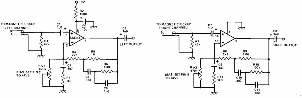
RIAA Stereo Preamplifier
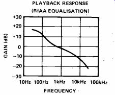
Records are cut with a frequency response such that when they are replayed with a magnetic pickup and a preamplifier with RIAA equalization (Recording Industry Association of America) the reproduced sound will be as similar to the original as possible.
The disc is cut at constant amplitude, except from 500Hz to 2120Hz where it is cut at constant velocity.
When this disc is replayed with a magnetic pickup, the relative output voltage rises with frequency, due to the fact that the magnetically generated voltage is proportional to the velocity of the stylus as it moves sideways in the groove. To restore the original sound quality, a preamplifier with a frequency response that gives decreasing output with increasing frequency is required. This response curve is known as the RIAA equalization and it is tailored accurately to fit the cutting and replay processes. The signal level from a magnetic pickup is low, generally 20mVpp and so a low noise pre amplifier is needed.
The circuit shows a realization of this requirement. The low noise amplifier is the LM381 made by National Semiconductors. A DC bias control is included (RV1, RV2), and the feedback components generate the RIAA curve.
Use screened cable for the wiring to the pickup, keep the circuit away from transformers (and the pickup and its wiring) and connect all the earths together, near to the IC.
++++++++++++++++++++
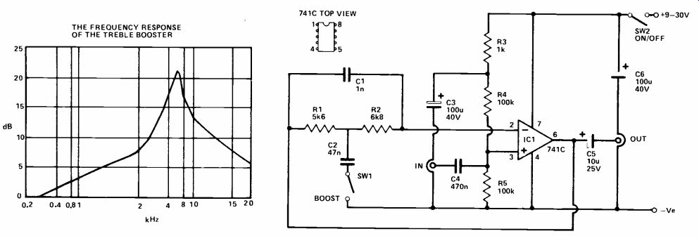
Treble Booster
A treble booster circuit can be used with an electric guitar (and also electronic instruments) to boost the higher order harmonics and give a more brilliant sound. A circuit of this type gives a fairly flat response at bass and most middle audio frequencies, with the upper-middle and lower treble frequencies being given a substantial amount of boost. It is normal to use only a modest amount of emphasis to the upper-treble in 'order to give good stability and a low noise level, and this also prevents the output from sounding too harsh. The frequency response is shown in the accompanying graph.
The circuit is basically an op amp used in the non-inverting amplifier mode. The non-inverting in put is biased by R4 and R5 via a decoupling network which is comprised of R3 and C3. C4 and C5 give DC blocking at the input and output respectively. With SW1 open there is virtually 100% negative feedback through R1, R2 and C1, giving the circuit unit gain and a flat response. Closing SW1 brings C2 into circuit, and this decouples some of the feedback through R1 and R2 at frequencies of more than a few hundred Hz, giving the required rising response. Feedback through C1 at high treble frequencies causes the response to fall away above about 5k5Hz, and prevents the very high frequency harmonics from being excessively emphasized.
+++++++++++++++++
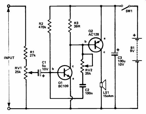
Simple Amplifier
The term "amplifier" covers a very wide range, from a one transistor preamp to an ultra sophisticated high power hi-fi system. There is little doubt that the circuit shown here is very simple. The output is in the order 250mW - quite sufficient for most purposes andcom parable to that of the average transistor radio. The distortion level is rather high, being about 5%.
The amplifier is also reasonably sensitive and will give full output with an input of about 50mV. Input impedance is about 50kR.
The slider from the volume control is connected to the base of Q1 via a DC blocking capacitor. Q1 is connected as a conventional common emitter amplifier with R2 providing the base bias and R3 acting as the collector load. This stage is directly connected to the second transistor which is a PNP type. In this way the current passing through Q1 provides the bias for the second transistor. The output of the second transistor is connected directly to the speech coil of the loudspeaker. This is not normally good practice since the standing current in the output transistor continually biases the coil either slightly in or out from its usual operating point. However if a large speaker is used, as it should be, this has very little effect and, since we are not aiming at hi fi, it does not matter.
The tone control comprises C2 and RV2 which are connected between the collector and base of Q1. At high resistance settings RV2 has little effect but on minimum settings the 100nF feeds back the high frequencies out of phase, thus cancelling them.
For this circuit to work properly, R3 must be selected with great care. The value shown here of 39 ohms is a typical one and, al though it may be used for initial setting up to ensure the circuit is operating, the value should be found by experiment. If it is too low there will be severe distortion at higher volume settings. If it is too high the current drain will be excessive even though the quality of reproduction will be good.
It is very important that Q2 is fitted with a heatsink as it will get very hot.
The speaker impedance is not all that critical and in the prototype speakers with an impedance as low as 8 ohms and as high as 80 ohms all worked well, although changing the speaker impedance will also necessitate a change in the value of R3.
+++++++++++++++++++++++
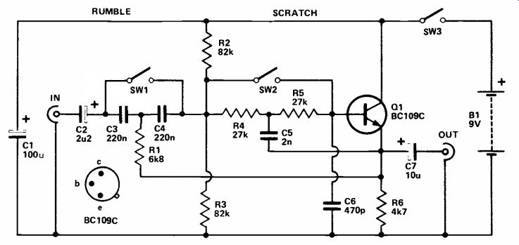
Scratch and Rumble Filter
This is a 12 dB per octave add-on scratch and rumble filter which can be connected into the 'tape Monitor' or some similar facility of the amplifier.
It is a conventional second order filter circuit having passive high pass filter formed by the series capacitance C3 and C4, plus the parallel resistance of R2 and R3 (the latter also being used to bias emitter follower transistor Q1). A passive filter of this type gives only a very slow initial roll off, and an ultimate attenuation rate of only 6 dB per octave. A bootstrap ping resistor is therefore used to improve performance. Above the cut-off frequency, where the gain of the circuit would otherwise fall off somewhat, R1 has the effect of reinforcing the input signal. Well below the cut off frequency, losses through C4 result in the signal level at Q1 emitter being well be low that at the junction of C3 and C4. This results in some of the signal at the junction of C3 and C4 being tapped off through R1, with C3 and R1 effectively forming a second high pass filter network.
This eliminates the slow initial roll off rate (in fact there is a small and insignificant peak of about 0.5dB above the cut off frequency) and speeds up the attenuation rate to a nominal 12dB per octave.
The low pass filter works in much the same way as the high pass one, except of course, the R and C filter elements have been transposed so as to give the correct filter action.
With the specified component values the rumble filter response falls below unity at approximately 45Hz, reaches the -6 dB point just above 30Hz, and then falls away at a nominal 12dB per octave. The scratch filter response crosses the unity gain point at about 6k5Hz, reaches the -6dB point at approximately 10kHz, and then falls away at a nominal 12dB per octave.
+++++++++++++++++++++
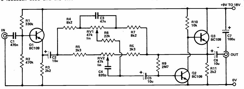
Cassette Preamplifier
Used in conjunction with one of the cassette mechanisms currently available on the surplus market (or a mechanism removed from an old recorder or player) this preamplifier circuit makes an inexpensive but useful cassette player for use with a hi-fi system.
The output signal level from a cassette tape head is typically about 500µV or so at middle audio frequencies for a mono head and about half this level for a stereo type. The preamplifier must, therefore, provide a considerable amount of voltage gain in order to match this to a hi-fi amplifier, since these require a signal level about 1,000 times higher. It is also necessary for the preamplifier to provide equalization, because the output from a tape head rises at a rate of 6dB per octave. However at higher audio frequencies, tape heads are not very efficient and require a much less rolloff.
Q1 and Q2 are used in a conventional two stage, direct coupled, common emitter amplifier and the frequency -selective negative feed back through C3 and R4 provides the appropriate equalization.
These also set the midband voltage gain of the input stage at about 46dB. With such a low input level it is obviously necessary to use low noise transistors (Such as the BC109C) in order to obtain good results. Running Q1 at a low collector current, about 200µA, also helps.
Q3 is used as a low gain common emitter stage, which provides the additional amplification.
R9 introduces negative feedback, which controls the voltage gain of Q3 and the specified value gives a gain of about 14dB. For a stereo unit R9 should be reduced to 390R in order to give increased gain, to compensate for the lower output of a stereo tape head.
When playing a Dolby B encoded cassette SW1 can be closed; this gives a small degree of treble cut which provides a reasonably flat overall response.
++++++++++++++++++
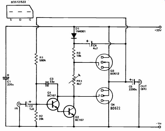
VMOS 10 Watt Amplifier
At first sight this circuit may seem to be a straightforward Class B de sign having an emitter follower, complementary output pair and Darlington Pair common emitter drive stage. However, the output divides are, in fact, complementary VMOS transistors used in the source follower mode (the FET equivalent of the emitter follower).
R1 and R2 are used to bias the unit to give the optimum quiescent output potential and they provide overall negative feedback, which improves the quality of re production. D1 and C4 are boot strapping components, enabling the gate drive voltage to Q3 to go above the positive supply potential, giving improved efficiency to the circuit. R3 is the main collector load for Q2 and PR1 is used to give a standing bias on the output transistors that gives a quiescent current consumption of about 25mA.
The thermal compensation circuitry normally used is totally unnecessary in this circuit, since VMOS devices do not suffer from thermal runaway. In fact the quiescent bias current will drop slightly as the output devices heat up, but not sufficiently to give rise to significant crossover distortion.
C2 and C5 provide DC blocking at the input and output respectively, while C1 is a supply decoupling component. C3 gives a degree of high frequency attenuation and aids the stability of the circuit.
Although the current in the driver stage, only about 1mA, may seem to be totally inadequate, it is in fact more than sufficient since the VMOS devices have extremely high input impedances and consume no significant input current.
This is one of their main advantages over bipolar devices. One disadvantage in this particular application is lower efficiency due to the higher threshold voltages and on resistance of VMOS transistors in comparison to bipolar devices.
However, the circuit will give an output of 10W rms using a supply voltage of about 33V or so (with a current drain of up to about 600mA). An input of about 500mV rms is needed for maximum output.
Note: The output devices do not have internal zener protection diodes and the appropriate hand ling precautions should be taken.
++++++++++++++++++++
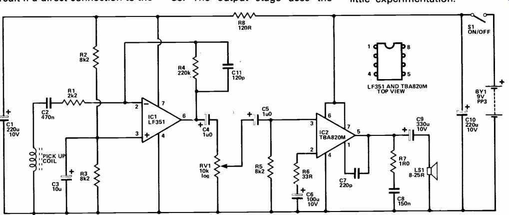
Telephone Amplifier
A telephone amplifier enables more than one person to follow a telephone conversation. The unit described here, in common with all normal units of this type, re quires no direct connection to the telephone. Instead, the special pick-up coil has a built-in rubber suction cap that enables it to be easily attached to the telephone base. This produces a very weak signal from the magnetic field radiated by an inductive component inside the telephone, but satisfactory results can be obtained if it is fed to low noise, high gain amplifier. It would of course be possible to use a much simpler circuit if a direct connection to the telephone were to be made, but this would make installation more difficult and it is ILLEGAL to make a direct connection to a Post Office telephone anyway.
The preamplifier stage of the unit is based on IC1 which is a low noise op amp having a FET input stage. This is used in the conventional inverting audio amplifier mode and the negative feedback network, R1, 4, sets the voltage gain at about 40dB. (100 times).
C11 reduces the gain slightly at high frequencies in order to obtain an improved signal to noise ratio.
C4 couples the output from the preamplifier to volume control, RV1, and from here the signal is coupled to the power amplifier by C5. The output stage uses the TBA820M, a class B amplifier which will give an output power of a few hundred milliwatts rms. The closed loop voltage gain of the device is determined by the value of R6, about 25dB. (180 times) with the specified value. This gives the required very high overall gain in conjunction with the preamplifier's gain. C7, R7 and C8 are needed in order to maintain stability.
The quiescent current consumption of the unit is only about 5mA, but this rises to as much as 50mA or so at high volume levels. The best position for the pick-up coil on the telephone base (not the handset) can be located with a little experimentation.
++++++++++++++++++
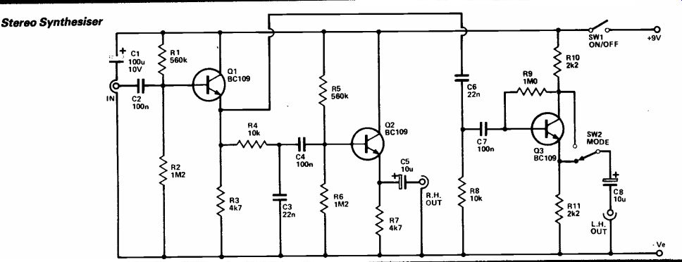
Stereo Synthesizer
There are two common methods of producing a pseudo stereo effect from a mono signal; playing the mono signal from the two speakers in antiphase, and the use of frequency selective techniques which normally consists of directing lower frequency signals into one channel and higher frequency signals into the other. This circuit uses the second technique, but can additionally give antiphase signals which can give a better effect, especially when using headphones.
Q1 is used as an emitter follower buffer stage which ensures that the two filter networks fed from its output are driven from a low impedance source. If these were driven direct from the input, it is quite possible that they would be fed from a source impedance of a few kilohms or more, which would be quite sufficient to alter their effective characteristics.
The two filters are formed by R4 and C3 (low pass), and C6 plus R8 (high pass). A high roll off rate is by no means essential in this application and the 6dB per octave attenuation rate of simple RC filters such as these is perfectly adequate. The-3dB point of each filter is at approximately 800Hz and the combined output of the filters, therefore, gives a virtually flat response with no significant peaks or troughs.
Q2 is connected as an emitter follower buffer stage and this ensures that there is minimal loading on the tow pass filter. Q3 similarly ensures that there is minimal loading on the high pass filter, but this device is also used as a phase splitter. With SW2 switched to take the output from Q3's emitter, Q3 effectively operates as an emitter follower and gives no phase inversion. With SW2 switched to take the output from Q3's collector, 03 then effectively acts as a common emitter stage with 100% negative feedback (and unity voltage gain) due to R11. It also provides a 180° phase shift so that the two output signals are in anti-phase. An in -phase relationship is needed to give a good central stereo image and the use of anti-phase signals tends to give an impression of increased channel separation.
In a stereo orchestral recording, it is normal for the violins to come from the left hand channel, with the cellos and basses from the right hand channel. Therefore, the high frequency signals are fed to the left channel and the low frequency signals are fed to the right channel so that the unit provides a similar effect (although it will obviously function properly with the 'outputs connected either way).
+++++++++++++++++
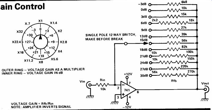
Preamp With dB-Stepped Gain Control
A handy little piece of test equipment is a preamplifier with stepped gain control selected by a rotary switch. The circuit here uses a single IC, 14 resistors and a single -pole, 12 -way rotary switch.
The voltage gain of an op -amp is determined by the ratio of Rfb/Rin; thus by having Rfb switched, the voltage gain can be varied. The input impedance of the preamplifier is set by Rir, to 10k.
+++++++++++++++++
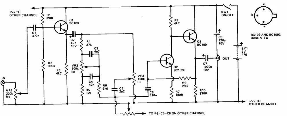
Headphone Amplifier
This simple stereo amplifier will drive a pair of stereo headphones, and can take its input from either a tuner or cassette deck.
The circuit shown here is for one channel, all the components being duplicated in the other channel except for S1, BY1, and VR4, which are obviously common to both channels. The two VR1s are a dual gang component, as are the two VR2s and the two VR3s.
The input signal is applied to volume control VR1, and from here it is coupled to a buffer stage based on Q1. This gives the unit a reasonably high input impedance of at least 100k. Its output feeds a conventional passive tone control circuit that can give bass lift or cut using VR2, and treble lift or cut using VR3. VR4 is used in the standard balance control arrangement. The output from the tone controls is coupled by C6 to a two stage direct coupled amplifier.
This uses Q2 in the common emitter mode to give sufficient voltage gain for an output level of up to about 2Vrms from most sources.
Q3 is an emitter follower buffer stage which matches the output from Q2 to the relatively low impedance of the headphones.
+++++++++++++++++++++
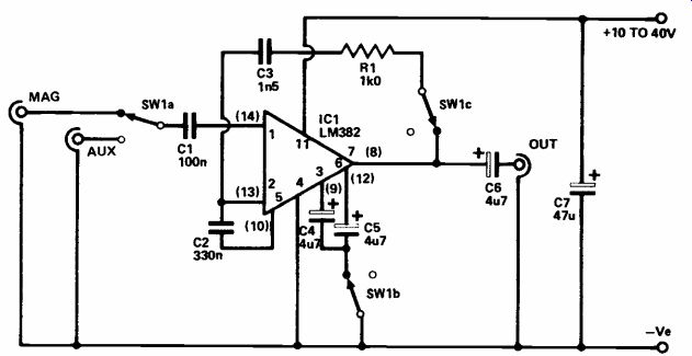
Simple Preamplifier
This preamplifier has two inputs; one for a magnetic cartridge and the other is an "Aux" input for a tuner, tape deck, etc. Although the circuit is very simple, it uses an IC which is specifically designed for this application and provides low levels of noise and distortion. The unit is suitable for stereo operation and both the required amplifiers are contained within a single LM382 IC.
The circuit diagram is for one channel only, but apart from the IC pin connections the other channel is identical. The numbers in brackets show the pin connections for the other channel. The supply connections of IC1 are common to both channels.
The LM382 has an internal biasing circuit which sets the quiescent output voltage at approximately 6V and no discrete biasing components are required. C6 provides DC blocking at the output.
When switched to the "Mag" mode, external feedback components are required to shape the frequency response characteristic of the amplifier in the required way. Bass cut and treble boost are applied to the signals transferred onto records so as to prevent excessive low frequency groove modulations and give an improved signal to noise ratio. The pre -amplifier must give corresponding bass boost and treble cut in order to give a flat overall frequency response. C2, C3 and R1 are the discrete feedback components and the LM382 itself contains some feedback resistors. C4 and C5 provide DC blocking for two shunt resistors in the feed back network.
When switched to the "Aux" mode, most of the feedback components are not required and are switched out of circuit by SW1a and SW1c. C2 is left in circuit, but is superfluous. In this mode the circuit has a voltage gain of only about four and is really just operating as a buffer stage. SW1a connects the input of the amplifier to the appropriate input socket and C1 provides DC blocking at the input. Of course the input wiring must all be screened to prevent stray pick-up of mains hum, etc.
The current consumption of the circuit is about 12.5mA. Due to the high supply ripple rejection of the LM382, it is not necessary to have a highly smoothed and decoupled supply.
++++++++++++++++++
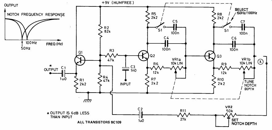
Hum Notch Filter
Magnetically induced hum is generally at a frequency of 50Hz, while ripple hum is mainly at 100Hz.
This circuit can deal with either type with switch selection of 50Hz or 100Hz operation.
The filter consists of two transistor stages which each delay the signal by 90°. The total delay through Q2 and Q3 is therefore 180° at point X. The delay only affects the hum part of the signal and this delayed (or rather, phase shifted) hum is mixed back into the main signal via RV2. The hum in the main signal is cancelled by the 180° shifted hum, and the other (wanted) signal, is virtually unaffected. RV1a, b is used to vary the centre of the notch frequency by plus or minus 40%. With the switch open circuit the frequency of operation is 100Hz.
++++++++++++++++++
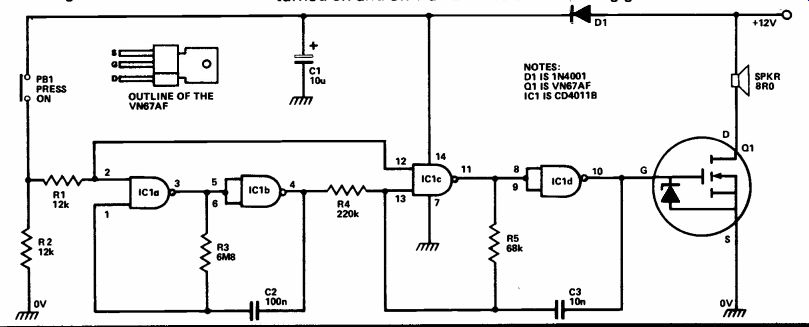
6 Watt Siren
This nifty little design uses the very latest advances in semiconductor technology to implement a very compact, inexpensive, yet exceptionally powerful alarm -sound generator unit that can easily be incorporated into an existing burglar alarm system or similar "security" device.
The alarm circuit incorporates a basic alarm-signal generator, followed by a power amplifier stage.
The alarm-signal section of the unit is designed around an inexpensive CMOS integrated circuit that consumes virtually zero "standby" power. The power amplifier stage is a real state-of-the art device, a low-cost VMOS power FET which also consumes virtually zero current when in "standby" mode. Consequently, the unit does not need a separate on/off switch and can be left permanently connected to a 12-volt battery supply.
IC1a and IC1b are wired as a slow astable multivibrator and 1C1c-IC1d are wired as a fast astable. Both these astables are "gated" types, which can be turned on and off via PB1. The output of the ICa-IC1b slow astable is used to modulate the frequency of the 1C1c-IC1d fast astable, and the output of the fast astable is fed to the external speaker via the Q1 VMOS power amplifier stage.
Normally, with PB1 open, both astables and Q1 are inoperative and the circuit consumes virtually zero standby current. D1 and C1 are used to ensure that the astable actions are not adversely influenced by voltage transients induced into the battery supply leads via the speaker. Note that the speaker used in the system must be an 8R0 type with a power rating greater than 6 watts.
++++++++++++
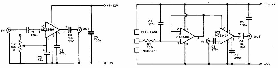
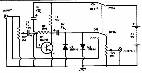
Remote and Touch Volume Controls
The MC3340P IC can be used as the basis of a remote volume control, as shown in the first circuit. RV1 controls the voltage gain of the MC3340P, which varies from typically 13dB at minimum resistance to about -80dB at maximum resistance. Since only a DC level is controlled by RV1, any AC pick-up in the connecting cable can be filtered out, which is the purpose of C2. C1 and C4 are input and output DC blocking capacitors respectively. C3 rolls off the RF response of the circuit to aid stability and prevent RF breakthrough.
The MC3340P can be used as the basis of a novel touch operated volume control, as shown in the second circuit. The device is controlled by a voltage rather than a resistance and gives the same attenuation range as the previous circuit.
The control voltage is obtained from a charged capacitor (C1) via an op -amp unity gain buffer stage utilizing IC1. ICI has a CMOS input stage which produces a typical in put resistance of 1.5 million Meg ohms. This ensures the charge on C1 is not significantly affected by the circuit; once set, it remains virtually unaltered for a long time.
The charge on C1 is set by the operator who, touching the lower and his or her skin resistance. This decreases the control voltage fed to IC2, and increases the volume.
Touching the upper two contacts causes C1 to gradually discharge; increasing the control voltage and decreasing the volume. When the unit is switched off, C1 gradually discharges. At switch -on it is necessary to bring the volume up to the required level, rather like using an ordinary combined on/off switch and volume control.
Both circuits will handle input levels of up to 500mVrms, with a THD figure of about 0.6% at high volume settings, rising to about 2% or so at low settings.
(adapted from: Electronics Digest (Vol. 2 No. 3--WINTER 1981))
NEXT: Indicators and Alarms