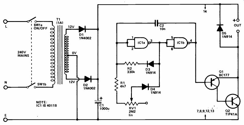
12V DC Motor Speed Controller
This motor speed controller is of the type where the motor is fed with a series of pulses of fixed du ration and the power fed to the motor is varied by altering the frequency of the pulses. The higher the frequency, the greater the power fed to the motor, up to the point where there is virtually no gap between the pulses and the motor is operating at full speed. A useful characteristic of this type of controller is that it gives relatively good results at low speeds and wastes little power with consequent low dissipation in the circuit. This circuit is for 12V DC motors having a maximum current consumption of up to 1A (or 2A if the secondary current rating of T1 is raised accordingly.
T1, D1, D2 and C1 form a simple DC supply which gives a loaded voltage of just over 12V (just over 17V unloaded). This is used to drive a CMOS astable multivibrator which is based on two of the gates in a 4011B device. The two gates that are used each have their inputs connected together so that they act as inverters and are connected in what is basically the standard CMOS astable circuit.
The circuit differs from the standard configuration in that there are two timing resistances; one formed by R2 and the other by the series resistance of R1 plus RV1.
D3 and D4 are steering diodes. In effect, R2 forms the timing resistance when the output of the astable is high and gives an output pulse of fixed duration. RV1 and R1 act as the timing resistance when the astable's output is low and the duration between output pulses can, therefore, be varied using RV1.
With RV1 at minimum there is a negligible gap between the output pulses, giving maximum speed from the motor. Increasing the resistance of RV1 increases the du ration between the pulses, giving decreased average output power or no significant output power at all with RV1 at maximum resistance.
Since the astable has only a low output current capability, the motor must be driven via a buffer amplifier. This uses Q1 and Q2 in the common emitter mode, with 100% overall negative feedback so that unity voltage gain (but a high current gain) is obtained.
+++++++++++++++++
Thyristor Switching
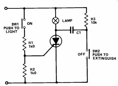
In this circuit, the thyristor is triggered by the action of the push button switch - note the 1k resistor (R2) which prevents the gate from being triggered by stray radiated pulses. Once the thyristor has been triggered on there is a low -resistance conducting path between anode and cathode, so that the voltage across the thyristor is low, not much above the minimum holding voltage at which the thyristor switches off.
The switch-off method uses a large -value capacitor C1 which charges up when the thyristor conducts. During the time that the thyristor conducts, the capacitor has one plate at supply voltage and the other at the low voltage of the thyristor anode. When the OFF switch is momentarily depressed, the plate of the capacitor which was at supply voltage is suddenly connected to zero volts. The other plate will follow it, dropping from about 0V2 to a negative voltage for a few milliseconds. This is time enough to allow the thyristor to become non -conducting. By the time the capacitor has re -charged, the thyristor is off.
This method works well when the load has a fairly high resistance (such as a low voltage lamp) and when a large value capacitance can be used. The capacitor, should be a paper or plastic type, because electrolytics do not take kindly to having their plates at re verse polarity, which will happen if the OFF switch is kept closed while the capacitor re-charges through the load.
++++++++++++
Nicad Current Generator
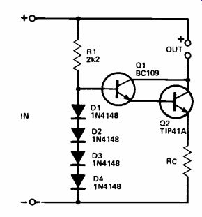
This simple add-on circuit enables a DC bench power supply to be used as a Ni-Cad charger. These cells have a low internal resistance and can be damaged if the charge current is significantly higher than the figure recommended by the manufacturer. Furthermore, the cell voltage increases as charging progresses, making it necessary to steadily increase the charge voltage if the charge current is to be maintained.
This unit is a constant current generator circuit which limits the current fed to the Ni-Cad cell(s) to an acceptable level. In effect, the unit automatically adjusts the charge voltage to just the right level to give the desired charge current. The circuit is a standard constant current generator configuration with R1 and D1-4 being used as a sort of low voltage zener stabilizer. About 0V7 is developed across each of the four forward biased silicon diodes, giving a total zener voltage of about 2V8.
Q1,2 are used as a Darlington pair and, therefore, have a very high combined gain so that quite high output currents can be produced by the fairly low drive current available. About 0V65 is dropped across the base-emitter terminals of both Q1 and Q2, giving about 1V5 across emitter resistor RC.
The emitter current can be controlled by RC. The collector current of Q1,2 is virtually identical to the emitter current and is actually just fractionally lower as the emitter current is equal to the sum of the base and collector currents. Thus, provided a low impedance load (such as Ni-Cad cells) is present at the output, the current fed to the load can be set by giving RC the appropriate value.
The value of RC is equal to 1,500 divided by the required output current in milliamps and would, for example, be 10R for rapid charge Ni-Cads requiring a charge current of 150mA (1,500 divided by 150 = 10R).
The input voltage should be 3-6V more than the total voltage of the cells being charged. The cells should be connected in series across the output. Of course, the power supply must be capable of supplying the charge current drawn by the cells plus the additional few milliamps drawn by the current generator circuit itself. For charge currents of more than about 100mA it will probably be necessary to fit Q2 with a small finned heatsink to prevent it from overheating.
+++++++++++++++++++
Thermostat
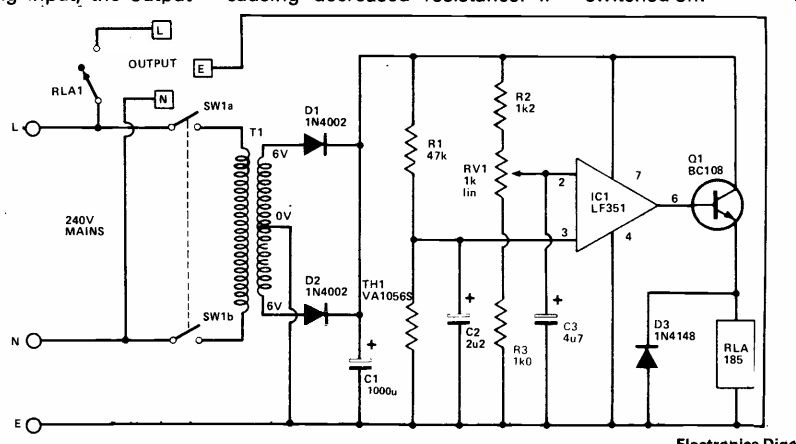
This simple thermostat will stabilize temperatures to within a fraction of one degree Centigrade. It covers a range which extends from a few degrees C to over 35 degrees C and is therefore suitable for use as a room thermostat, a thermostat for photographic solutions, etc.
The circuit uses operational amplifier IC1 as a voltage comparator. If the voltage at its non-inverting input is higher than that at the inverting input, the output goes to almost the full positive supply voltage. If the comparative input states are reversed, the output assumes a very low voltage.
The inverting input is fed with a reference voltage which is taken from the slider of RV1, acting as the temperature control. The non-inverting input is fed from a potential divider which consists of R1 and Th1.
Th1 is a negative temperature coefficient thermistor; its resistance varies according to tempera ture with increased temperature causing decreased resistance. If the voltage produced by Th1 and R1 is less than that set by RV1 slider, IC1's output will go high, switching on the relay via an emitter follower buffer stage, Q1.
Power is then connected to the heater and the room temperature (or whatever) starts to rise. This causes a reduction in the resistance of Th1, and the voltage fed to IC1's non-inverting input. This voltage soon falls below that fed to the inverting input, causing IC1's output to go low, the relay to de-energize, and the heater to be switched off.
+++++++++++++++++
Mains Interference Suppression
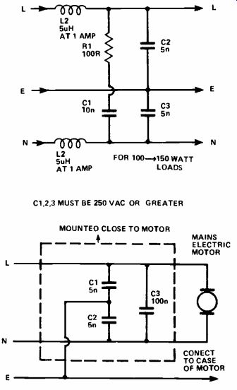
If you were to take a look at the mains voltage on an oscilloscope you might expect to find a 250 Vrms sinewave. If you do see a pure sine wave then you are quite lucky and need not read any further! However, most mains supplies are composed of the sinusoidal generated by the electricity company plus various forms of interference generated by local users. When light bulbs, electric ovens and various electric motors are turned on they usually cause clicks and spikes to be generated.
The worst offenders are large brush electric motors, thyristor dimmers and motor controls, spot welding units, in fact anything that grabs large chunks of current abruptly from the mains supply.
The clicks and spikes often make their way into electronic equipment, producing audible clicks on loudspeakers and generating errors in digital equipment. Faced with this problem there are two things that can be done: filter out the mains borne interference or try to prevent it being generated.
The top circuit shows a typical mains filter. The mains has to pass through a passive lowpass filter made up of an inductor and a capacitor, causing the high frequency parts of the interference to be attenuated. The inductor must have a high current rating (1 amp in this case), and the capacitors a high voltage rating (250Vac at least). This type of mains filter can be brought as a module for a few pounds, but it can also be made out of discrete components. In the latter case, use rubber sleeves on the connections.
The bottom circuit shows how to suppress motor generated interference and also reduce electromagnetic radiation. Again, the capacitors need to have a sufficiently large voltage rating, and take care to insulate all connections.
++++++++++++++++++
Fast Fuse
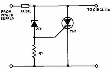
It may look a bit daft using a thyristor to blow a fuse, but it has two important advantages. The most obvious one is fuses don't blow just because the voltage rises, so that a fuse doesn't protect the circuit against excessive voltage, it only protects the power supply against excessive current. The other point is that a fuse takes some time to blow, several milliseconds. That may not sound like a long time, but several hundred pounds worth of IC's can be destroyed in only a thousandth of that time. The thyristor operates faster, getting the voltage down as soon as it reaches danger level, and blowing the fuse so that some attention is called for. The name "crowbar" circuit is a good one--the action is pretty much the same as that of putting a crowbar across the supply voltage! In this circuit, Zener diode ZD1 has been selected so that it breaks down at 5V6. Now the normal voltage output of this circuit is 5V, and it's intended to supply a lot of IC's whose supply voltage must not rise much above 5V6.
What happens if the voltage does get too high? Simple - ZD1 conducts and triggers the thyristor. The thyristor can then conduct, shorting out the power supply and causing the fuse to blow. Once the fuse has blown, there's no voltage in the circuit, and the thyristor instantly resets, ready to resume protection duty when the fault that caused the trouble is sorted out.
++++++++++++++++
Two-Down–One
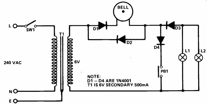
This circuit was designed so that people who have an illuminated door -bell can run a separate bulb over the door number without the need for a second set of wires from the transformer. If you try to use the same pair of wires to run a second bulb the increase in current will probably make the hammer of the bell 'tremble'. By using only one half of the AC cycle from the transformer to illuminate the bulbs whilst the other half of the cycle rings the bell, the problem is overcome.
+++++++++++++++
Ni-cad Charger
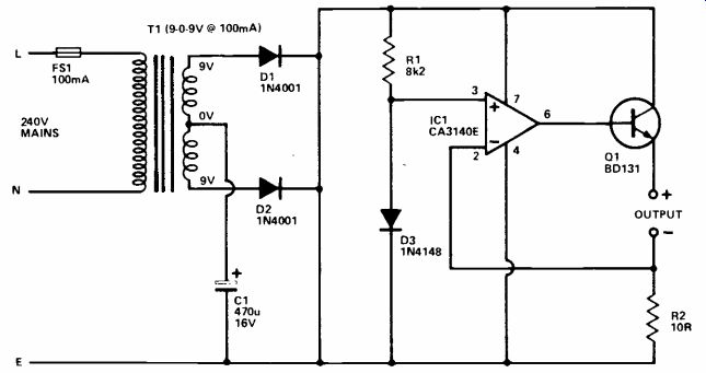
A special charger is needed for NiCad calls because they have a very low internal resistance, leading to an excessive charging current even if the applied voltage is only marginally too high.
In this circuit, T1, D1, D2, and C1 form a conventional stepdown, isolation, fullwave rectifier, and smoothing circuit. The other components provide the current regulation. IC1 is used as a comparator with discrete buffer stage Q1 giving a suitably high output current capability for this application.
IC1's non-inverting input is fed with a 0V65 reference potential provided by R1 and D3. The inverting input is taken to earth by R2 under quiescent conditions, causing the output to go fully positive.
With a NiCad cell connected across the output a high current will attempt to flow, causing the voltage across R2 to increase. It can rise to only 0V65. However, as a higher voltage reverses the comparative input levels to IC1, resulting in the output going lower and reducing the voltage across R2 towards 0V65. The maximum output current (the charge current) is therefore the current produced with 0V65 across 10 ohms, or 65 mA, in other words.
Some AA NiCad cells have a maximum recommended charge current of about 45 or 50 mA, and for these types R2 should be increased to 13 ohms in order to obtain the appropriate charge current. Some rapid charge types will take 150mA, and this requires reducing R2 to 4.3 ohms (3.3 ohms plus 1 ohm in series if a suitable component cannot be obtained).
T1 should be changed to a type having a current rating of 250 mA, and Q1 should be fitted with a small bolt -on finned heatsink. The unit can charge up to four cells (six, if T1 is made a 12V type), and these must be connected in series across the output, not in parallel.
++++++++++++++++++++++
Overload Current Trip
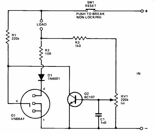
This overload current trip can be used between the powered equipment and the power supply and will cut off the supply almost instantly if a preset threshold current is exceeded. The trip current can be varied from just a few hundred milliamps. The unit will work with supply voltages of 5-40V.
When power is first applied to the circuit, power FET Q1 will be biased hard into conduction by bias resistor R1. Power is, therefore, supplied to the load via Q1, D1 and R2. There will be a voltage drop across these components, and to some extent this varies with changes in the supply current. At low output currents there is likely to be a voltage drop of something in the region of OV7, but this increases to a volt or so at high currents.
RV1 is adjusted so that at output currents below the required threshold level the proportion of the voltage dropped across Q1, D1 and R2 (and fed to Q2's base terminal) is not sufficient to switch on Q2. If the threshold current is exceeded, the voltage fed to Q2's base is then adequate to switch the device on and it diverts the bias current that formerly went to Q1's gate terminal. Q1 then switches off and cuts the supply to the load. Q2 remains switched on as it receives a strong base bias from the positive supply through the load, current limiting resistor R3 and RV1. Once tripped, the circuit thus latches in the "off" state.
It can be returned to the "on" state by clearing the overload and then briefly operating SW1 so that the supply is momentarily disconnected from the unit. When the supply to restored it then starts at the "on" state once again. C1 ensures that the circuit always initially assumes the correct state and also helps to prevent spurious triggering of the unit.
When using the unit it should be kept in mind that about 1V is lost through the device and the output voltage from the supply must be adjusted to compensate. The current trip inevitably causes some loss of regulation efficiency, but this is only marginal. If the unit is to have a trip current of 100mA or more, R2 can be reduced to about 1R8 in order to maintain the low voltage drop and marginal degradation of regulation efficiency.
(adapted from: Electronics Digest (Vol. 2 No. 3--WINTER 1981))
NEXT: Radio