Simple Voltage Regulator
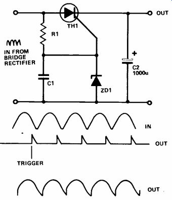
This is a voltage adjuster which enables you to obtain several switched values of DC voltage from a transformer without using tappings. It's particularly useful for lead-acid (car or motorbike) battery charging, as the voltage is so easy to change. The principle is that the zener diode, which may be one of several selected by a switch, applies a steady voltage, equal to the zener diode voltage, to the gate of the thyristor. At the anode of the thyristor, the wave form is a full-wave rectified voltage from the bridge rectifier. The cathode of the thyristor is connected to the reservoir capacitor C2, a large value electrolytic rated at the full peak voltage of the transformer secondary.
To see what happens, imagine that the peak voltage of the rectified wave is 25V and that we have a 15V zener diode. When the circuit is first switched on, capacitor C2 is uncharged, so that the cathode voltage of TH1 is zero.
When the voltage at the anode starts to rise the thyristor will not conduct right away, because C1 has to be charged up first. As C1 charges, however, TH1 will switch on, so that current flows, charging C2 to the full peak voltage.
Now if there is no load resistor connected across C2, the thyristor will not conduct again even if it is triggered, because the anode voltage will not be any higher than the cathode voltage. Any normal power supply is used with a load, however, so that we can assume that the voltage across C2 will drop quite a bit between the time of the first voltage peak and the next one. If the voltage across C2 is higher than the zener diode voltage though, the thyristor will not trigger, and the next voltage pulse does not cause the thyristor to conduct.
This continues until the output voltage drops to less than the voltage of the zener diode. When this happens, the thyristor will start to conduct whenever the anode voltage is higher than the cathode voltage, and the reservoir capacitor C2 will once again be charged to the full peak voltage.
The thyristor will conduct every now and again; enough to keep the average voltage at the output fairly steady at around the zener diode voltage.
If this circuit is used as a battery charger (lead-acid only) then C2 can be omitted.
To change output voltage, just switch in another zener diode! The output is not easy to smooth to an acceptable standard for most electronics equipment, but is ideal for battery charging or running lights or motors.
+++++++++++++++++
Single IC Power Supply
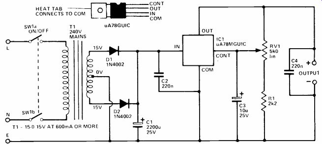
The unit described here has an output voltage variable from 5 to 15 volts, and a maximum output current of 500mA. The output is extremely well stabilized and noise is well below 1 mV.
The mains supply is connected to the primary winding of isolation and step-down transformer T1 through on/off switch SW1. The centre tapped secondary of T1 feeds a standing fullwave rectifier and smoothing circuit which uses D1, D2 and C1.
IC1 is the voltage regulator chip, and has four terminals. The unregulated input voltage is applied to the "IN" and "COM" terminals, while the stabilized output is taken from the "OUT" and "COM" terminals. The fourth terminal is "CONT" (Control) and if this is fed from the output, via a potential divider, negative feedback action will stabilize the voltage at this terminal at a nominal level of 5 volts.
In this case the potential divider is formed by RV1 and Al. If RV1 slider is at the top of its track the output will be stabilized at 5 volts.
A higher voltage would take the "CONT" terminal (which is now directly connected to the output) above 5 volts, causing the error to be sensed and corrected.
Similarly, a lower voltage would take the "CONT terminal below 5 volts, causing the output to swing more positive.
If RV1 slider is moved down its track, the voltage fed to the "CONT" terminal will decrease, sending the output higher in order to return this potential to 5 volts.
Thus RV1 can be used to vary the output voltage, with a maximum potential of about 16 volts or so appearing at the output when RV1 slider is at the bottom of its track.
Above this level, at high output currents, there will be insufficient input voltage from the rectifier and smoothing circuit to properly maintain the output voltage.
The regulator device has built-in foldback current limiting which prevents the output from much exceeding 500 mA in the event of a minor overload. Stronger overloads result in decreased output current, the short circuit current being about 200mA! Decoupling capacitors C2 and C3 should be mounted physically close to IC1, which must be mounted on a substantial heatsink.
+++++++++++++++++++
Supply Splitter
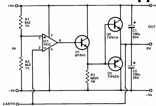
Many operational amplifier based circuits require dual balanced power supplies, and cannot be powered direct from workshop units which have only a single output. An add-on unit, such as the circuit shown here, can be used to produce a low impedance centre tap on the output of a workshop power supply. If this centre tap is connected to the earth socket of the power supply, and made the OV rail, the positive and negative rails will be at equal potentials relative to the OV rail, but of opposite polarity. Thus the dual balanced positive and negative rails are provided, but each output rail is, of course, at a potential of only half the input voltage. In other words, for an output of (say) ± 15 volts it is necessary to feed 30 volts into the input.
This circuit will operate with in put voltages of between 9 volts and an absolute maximum of 36 volts, and can handle output currents of up to about 500mA or so.
The quiescent current consumption is 8 to 25mA depending on the input potential.
Basically the circuit consists of a potential divider circuit (R1 and R2) to produce an accurate potential of half the input voltage, and a buffer amplifier which is fed with this voltage and produces a low impedance output at the same potential. The buffer amplifier uses operational amplifier IC1 driving emitter follower stage Q1, which in turn drives complementary emitter follower stage Q2, Q3.
There is 100% negative feedback from the output at Q2 and Q3 emitters to the inverting input of IC1 giving the amplifier unity voltage gain. The high gain of the circuit plus the negative feedback gives a low output impedance so that loading of the output does not pull the 0V rail significantly off centre. A complementary output stage is used as this gives low quiescent current consumption.
If the unit is used at currents of more than about 100mA, Q2 and Q3 will probably need to be fitted with heatsinks to prevent them from overheating.
+++++++++++++++++++
Regulated Power Supply
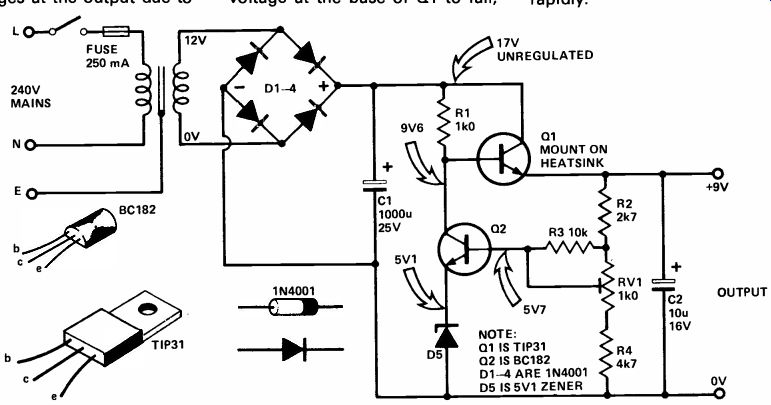
Two transistors and a voltage reference can be used to make a regulated power supply. Transistor Q1 is used as the power control element and so must be mounted on a heat sink. Q2 provides negative feedback and so helps iron out any changes at the output due to fluctuating load conditions or variations in the unregulated rail.
The circuit operation is as follows: the current through Q2 and D5 sets up a voltage of 5V1 across D5.
The base of Q2 is connected to the output by resistors R2, 3, 4 and RV1. If the output voltage rises, then more current will flow through Q2. This causes the voltage at the base of Q1 to fall, which in turn reduces the output.
RV1 is used to set up the output voltage to +9V. If the wiper of RV1 should accidentally lift off, the output voltage would instantly rise to that of the unregulated rail. To prevent this, R3 provides a permanent DC path to the base of Q2. C2 helps to improve the regulation when the load conditions change rapidly.
++++++++++++++++++++++++
5-13V Power Supply
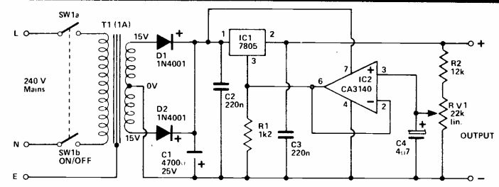
Although three terminal voltage regulators are often referred to as "fixed" voltage regulators, they can actually be used to provide output voltages other than their nominal ones, and can even be employed in variable voltage power supplies, as in the circuit shown here.
The three terminals of these voltage regulators are the input (pin 1), output (pin 2), and common (pin 3). The input voltage is applied to pins 1 and 3 with the correct polarity, and the stabilized output is extracted from pins 2 and 3. In effect, the device is actually stabilizing the voltage on pin 2 at some fixed level above the potential at pin 3. Normally pin 3 is at OV, and so the output voltage is determined by the nominal output voltage rating of the regulator.
Voltages greater than that for which the device is intended can be obtained simply by raising the pin 3 voltage by the appropriate amount. For example, a 5V regulator can be made to give a 9V output if its common terminal is taken to a potential of 4V. In this case a 5V regulator is used, and its common terminal is taken to a variable voltage of about 0 to 8V or so. This gives an output which is variable from about 5 to 13V. The voltage is supplied by R2 and RV1 which are connected across the stabilized output so that regulation efficiency is not significantly impaired. This voltage is at too high an impedance to directly drive pin 3 of IC1, and so a simple buffer amplifier based on IC2 is interposed between the two. R1 is a ballast resistor. A CA3140 device has been chosen for the IC2 position since the output of this device can swing to within a few milli volts of the negative supply voltage. Many alternatives such as the 741C device have a minimum output voltage of about 2V, which would give the power supply a minimum output voltage of approximately 7V, thus rendering the unit unsuitable for use with TTL and many other types of circuit.
The input voltage for the regulator circuit is derived from a conventional push-pull type step down, rectifier, and smoothing circuit. C2 and C3 aid the stability of the circuit and should be mounted physically as close to the regulator IC as possible. C4 provides' smoothing of the voltage at RV1 slider, and helps to give the circuit a low output noise level of about a millivolt or so. Regulation is also very good, the output falling by only 70mV between zero load and full output. The 7805 IC has current limiting circuitry which prevents an output current much in excess of 1A from flowing.
++++++++++++++++++
Car Cassette Power Supply
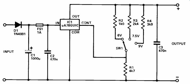
When using a portable cassette recorder in a car or boat it is far cheaper to run the unit from the vehicle's battery than from internal batteries. This circuit will give an output of 6, 7.5, or 9V from a nominal 12V input with- a maximum output current of 1A.
It uses a four terminal monolithic voltage regulator to give the voltage stepdown and provide a well stabilized output. The input to the regulator is obtained via D1 which blocks the supply if it is connected with the wrong polarity, and fuse FS1. The input will probably contain a certain amount of noise which is smoothed by C1. C2 and C3 are decoupling capacitors which aid the stability of the circuit, and should be connected as close to IC1 as possible.
The output voltage of IC1 is set by a potential divider connected across the output and feeding into IC1's CONT (control) terminal. A negative feedback action stabilizes the voltage on the CONT terminal at 5V, and the output at a level equal to 5V plus the potential dropped by the potential divider.
The value of R1 sets the potential divider current at just over 1mA, giving a drop of about 1V across R2, 2V5 across R3, and 4V across R4. SW1 can thus be used to select output voltages of 6V, 7V5, and 9V by switching the appropriate resistor into circuit. If only a single output voltage is required, SW1 is omitted and the appropriate resistor is connected between IC1's CONT terminal and the output.
IC1 must be mounted on a heatsink, and this can be the case, if a metal type is used. The heat-tap of the device connects internally to thecom terminal, so the tab must be insulated from the case in the usual manner if the latter is earthed and the unit is installed in a positive earth vehicle. The uA78GU1C has thermal overload protection circuitry and foldback output current limiting incorporated in its design.
++++++++++++++++++++
Power Supply With IC Regulator
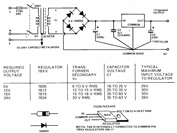
A regulated power supply used to require a fairly complex circuit but the introduction of special ICs has made matters much simpler.
The chart shows the various voltage requirements for four types of voltage regulator. Care must be taken that the voltage ratings of the regulator are not exceeded, as this can blow up the IC.
The secondary voltage from the transformer (it must be an isolating transformer but most are) is full-wave rectified by the diodes and then smoothed by capacitor. The voltage here is unregulated and has AC ripple superimposed upon it. The IC removes this and gives an almost ripple free, stable DC voltage. C2 and C3 must be sited close to the regulator to prevent any loss of performance due to high frequency instability.
Note that the capacitor and common lead from the IC should be wired to the same point, this helps to reduce instability and hum problems that can occur due to poor layout.
The 78XX series of regulators come in a TO220 package generally can supply 500mA.
Therefore the maximum power dissipated in them is probably going to be 500mA times the voltage difference between the in put and output terminals. This might mean that the regulator has to dissipate 5W of heat, therefore an adequate heatsink must be used. The 78XX series is current limited which means that if the maximum current is exceeded, the output voltage drops towards 0V.
The regulator is thus short-circuit protected as long as proper heat sinking is provided.
+++++++++++++++++++++++++
Regulator Booster
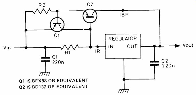
If you've ever been in the unfortunate position of having a regulator in a piece of equipment which will supply, say, 0.5 A and you find that, for one reason or another, the equipment needs to draw 2A then this little circuit may save the day.
Essentially, it consists of a transistor (Q2) which will switch on at a certain current into the regulator and bypass it to an extent. It is similar to ‘current dumping' amplifier; the transistor will pass a large amount of current without regulating it and the regulator will do all the fine tuning to make sure the output is stable. The circuit also includes a second transistor, Q1, which will limit the current through the Q2 during a short circuit of the output; the regulator will presumably look after itself.
The operation of the circuit is fairly simple. As soon as the voltage drop across R1 is greater than the minimum bias voltage for Q2 (0V6), Q2 will turn on. As R1 is 1 ohm, this will occur when 0.6A is passing into the regulator. Having switched on, Q2 will supply current directly to the load. The regulator will sense the output voltage and if (as is likely, since the current through Q2 will be un-regulated) the output voltage is not now what it should be it will pass or hold back current as required to maintain the output voltage. The two capacitors are necessary to prevent the whole thing from going into a frantic oscillation as the regulator and Q2 try to decide who is doing what.
If the current through R2 rises above that needed to provide an OV6 drop across it, Q1 will switch on and short out R1, thus removing the bias from Q2. This will prevent Q2 from passing more current than is good for it. Q2 should be mounted on a heat sink to prevent it from glowing.
+++++++++++++++
Unregulated Power Supply
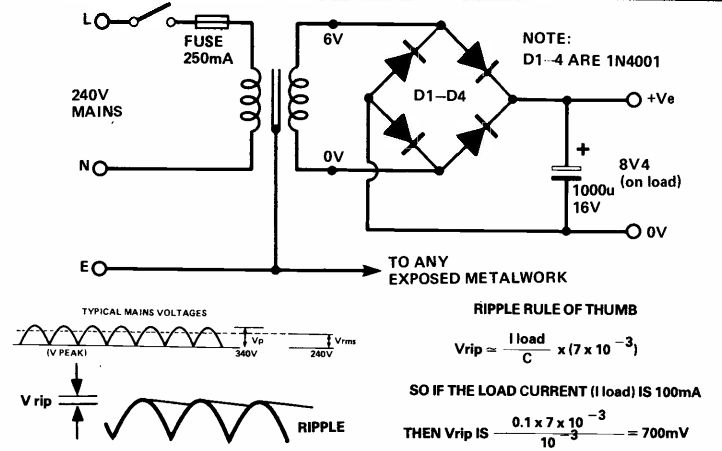
A single rail power supply is shown in the diagram above. For safety, the fuse is put in the live wire path to the transformer. Also, the live wire is connected to the 240V terminal of the transformer; this part of the primary winding is furthest away from the secondary and so increases the safety of the unit. The earth should be connected to any exposed metalwork and to the transformer screen, if it has one. The voltages quoted are AC voltages measured in Volts rms.
The output of the transformer is 6V rms on load. When the transformer is not loaded this voltage may increase by about 25%.
(adapted from: Electronics Digest (Vol. 2 No. 3--WINTER 1981))
NEXT: Power Control