555 IC Timer
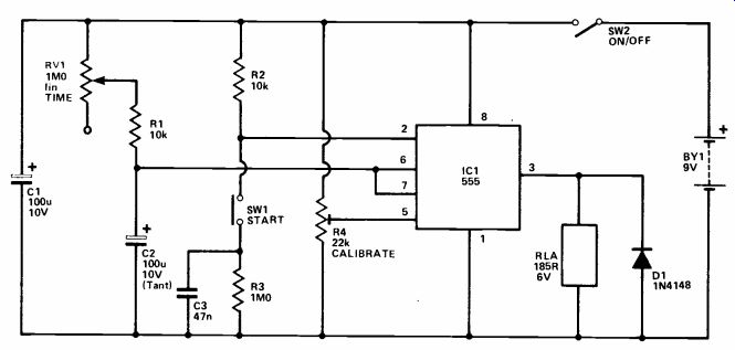
In the monostable multivibrator mode the 555 IC requires a trigger pulse which takes the trigger input below 1/3 of the supply voltage.
The normally low output then goes high for a period determined by a C-R network, the pulse length being approximately 1.1 CR seconds. However the output will stay high as long as the trigger (pin 2) is held below 1/3V+ This circuit is for a timer having a 1 to 100 second range, suitable for use as an enlarger timer, for example. It is triggered by depressing SW1, generating a brief negative pulse before C3 charges via R2. This makes it impossible to prolong the input pulse and produce a false output period by keeping SW1 depressed. C3 is quickly discharged by R3 when SW1 is released, rendering the trigger circuit ready for the next operation.
The tolerance of timing components RV1, R1, and C2 make it impossible to obtain a highly predictable time range, and this is overcome by the inclusion of R4.
Normally the output pulse ends when the charge on the timing capacitor reaches 2/3 V+. R4 can be used to raise or lower the threshold voltage, to extend or shorten the output pulse, to obtain the appropriate timing range.
++++++++++++++++
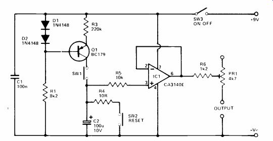
D.M.M. To Stopclock Converter
This simple add-on circuit can be used with a DMM switched to the 1mA range to give a stopclock having a range of 0-99s (or 0-199s for a 3 1/2 digit instrument). It can also be used with an ordinary analogue or multimeter or panel meter, giving a range of 1-100s, but the resolution will be lower than with a digital instrument.
The unit relies on the fact that a linear rise in voltage is produced across a capacitor if it is fed with a constant charge current. The capacitor (C2) must be a high quality type. The use of a tantalum bead component is, therefore, recommended. C2 cannot simply be charged from the supply lines via a resistor, since the voltage across the resistor would drop as the voltage across C2 increases. This would give a decreasing charge current as C2 charges exponentially and the required linear voltage slope would not be produced. C2 is, therefore, charged from a conventional constant current source which is based on Q1.
D1, D2 and R1 form a simple shunt regulator circuit which bias the base of Q1 approximately 1V3 be low the positive supply potential.
There is a voltage drop of about OV65 across the base emitter terminals of Q1, giving about 0V65 across emitter resistor R3. This gives an emitter current of roughly 3uA and, as the collector and emitter currents of a high gain device (such as the BC179 used in the Q1 position) are virtually identical, a constant charge current of about 3uA is fed to C2 when SW1 is operated. This low charge current together with the fairly high value of C2 produces a suitably long time constant.
It is essential that the voltmeter circuit takes no significant current from C2 as this would affect accuracy and would result in a decaying reading at the end of a timing run.
Operational amplifier IC1 is, therefore, used as a unity gain buffer stage which gives an input impedance of about 1.5 million megohms and ensures that there is no significant loading on C2. PR1 enables the sensitivity of the voltmeter circuit to be adjusted to the correct level. In practice, SW1 is depressed for (say) 90s and then PR1 is adjusted for the appropriate reading on the DMM.
SW2 is a reset switch and this discharges C2 (via current limiting resistor R4) if it is briefly operated. SW3 is an ordinary on/off switch.
+++++++++++++
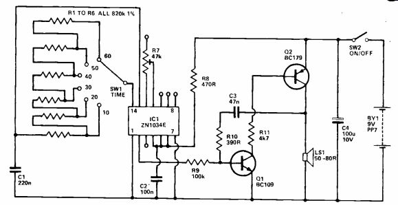
ZN1034E Timer
Long timing periods are difficult or even impossible to obtain using most simple timing circuits, such as those using the well-known 555 timer IC.
The problem is that such circuits usually provide a timing period of about RC seconds, and times of more than a few minutes require unrealistically high values for the timing resistor and capacitor.
The ZN1034E device is specifically intended for applications where long times are required, and by using an oscillator, a 14 stage binary divider (divide by 4,096 circuit), and a logic control section, an output time of between about 2,700 and 7,500RC seconds can be attained! Times of a few minutes to a few hours can be obtained without having to use an electrolytic timing capacitor, giving excellent reliability and accuracy.
This simple timer circuit provides an audible alarm at the end of the timing period which can be varied from 10 to 60 minutes in 10 minute increments. C1 is the timing capacitor, and the timing resistance is formed by which ever of the series of resistors (R1 to R6) is switched into circuit using SW1.
The timing resistors all have the same value, and so if one resistor gives a time of 10 minutes, two produce a time of 20 minutes, three give 30 minutes, and so on.
The timing period can be varied from about 2,700RC to 4,100RC seconds using R7, and in practice this is adjusted by trial and error to give a suitably high level of time accuracy.
The ZN1034E has an internal 5V shunt regulator, and R8 is the load resistor for this. The trigger input (pin 1) is connected to the negative supply so that circuit is triggered at switch on. The output at pin 2 goes low during the timing period, cutting off both Q1 and Q2.
These two devices, which form the basis of an audio oscillator driving LS1, are biased into operation at the end of the timing period when pin 2 goes high, causing the alarm to sound.
The circuit consumes about 8mA under quiescent conditions, rising to about 16mA when the alarm is operating. The times provided by the unit can be varied to suit individual requirements but the timing resistance should be no more than about 10 megohms, and the timing capacitance should not be less than 3n3.
+++++++++++++++++
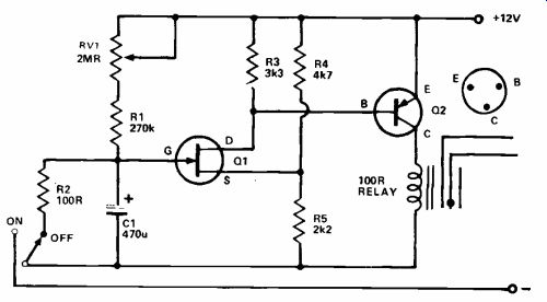
Timer
An adjustable timer, giving a delay of about 10 seconds to 1 minute, can be used for photographic and other purposes, or with various games where each competitor must make his move within the agreed period.
When the switch is moved to the "On" position, timing begins and C1 commences to charge through R1 and RV1. The two resistors R4 and R5 hold the source of Q1 at a fixed potential. When the voltage across C1 has reached a high enough level, Q1 gate is positive so that drain current flows through R3. This causes a voltage drop in R3, so that the base of Q2 moves negative. Q2 conducts and collector current flows in the relay coil, closing the relay contacts.
When the switch is returned to the "Off" position, C1 is discharged through R2, so that the interval can be repeated.
A 2N3819 is suggested for Q1, and AC128 for Q2. With C1 as shown (470uF) the interval was found to lie between 10 seconds with a total of 250k in the R1/RV1 position, up to 1 minute with 2 megohm. Increasing C1, R1 or RV1 will lengthen the interval. Smaller values here will reduce it. This was with current rising to 40mA, with a 100 ohm relay.
It is not of course essential that these values or transistor types be followed exactly, and other relays would also be practicable, provided Q2 allows a satisfactory current and voltage to suit the relay.
Generally, a relay with a coil resistance of about 100 to 250 ohms will be most satisfactory.
The relay contacts can be wired so that when the relay coil is energized, the circuit is completed, or interrupted. For games and similar purposes, a 12 volt 3 watt indicator lamp can be operated from the same 12V supply. Should any kind of mains -voltage circuit be controlled, the relay must be a type intended for this purpose, and care must be taken to arrange mains circuit so that no danger can arise for the user.
+++++++++++++++++++++++++
CMOS Monostable
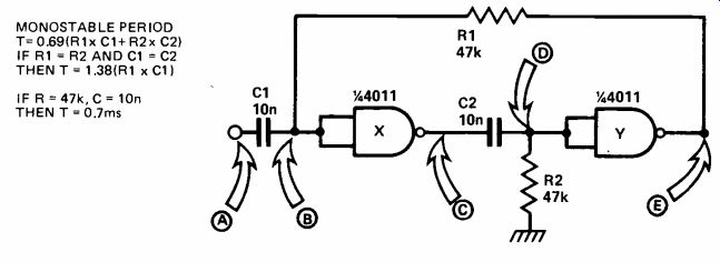
A monostable is an electronic circuit that generates an output pulse of defined duration when triggered by an input signal transition. The monostable action can be used for many different functions. For example, when a cheap push button is used to trigger digital devices, spurious pulses often find their way into the circuitry.
This is due to the contracts inside the button bouncing when it is pressed and released. Digital circuitry will regard all of the bounces as valid input signals and act accordingly--this can be disastrous in counting applications. A monostable can be used to de -bounce the push button; by setting the output pulse duration for a period longer than the longest expected bounce time, the bounces will have no effect on the main circuitry. So, with a simple monostable between each push button and the input circuitry, the digital devices are protected from the horrors of untamed push but tons.
Only two inverters are needed for a monostable circuit. Here we have used a 40116 quad NAND package, as they are even cheaper than a CMOS inverter package and work just as well.
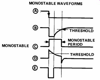
The monostable period is initiated by the transition of point A from positive to zero volts. This is called a negative-going edge.
Transition of point 'A' in the opposite direction (a positive-going edge) will have no effect.
A negative edge at 'A' causes point 'B' to go to zero volts momentarily. This will then drive point 'E' to zero and this will hold point 'B' at zero volts, even when the pulse at 'A' is finished. The circuit will stay in this state while C2 charges. When C2 is fully charged there will no longer be a current through R2 and point 'D' will fall to zero again. 'E' will go positive and so will 'B', after a time determined by the values of C1 and R1. Point 'C' will fall to zero and C2 will be discharged, ready for the next pulse from 'A'.
The length of time for which 'C' remains positive is determined by the values of C1, R1, C2 and R2. If either the resistance or the capacitance is increased, the time for which the monostable is triggered will increase.
The equations for calculating the monostable period are given on the circuit diagram Polarised capacitors should not be used, and the resistance value of R should be kept within the range of 10kR to 10MR.
+++++++++++++
Simple Timer
This general purpose timer gives an audible alarm some predetermined time after the unit is switched on. With the specified values the time is variable from about 30 seconds to 5 minutes, but this can be altered to suit individual requirements.
When the unit is switched on, C1 begins to charge via R1 and RV1.
Initially the voltage at the inverting input of IC1 will be higher than that appearing at the non-inverting input, and so IC1 output will assume a very low voltage. As C1 charges up, the voltage fed to the inverting input gradually falls until it starts to go below the voltage at the non -inverting input. IC1 output then begins to rise and due to coupling through R4 this increases the voltage at the non -inverting input. This causes a further increase in output voltage, and a re generative action takes place which causes IC1 output to rapidly swing to almost a full positive supply potential.
The 555 is used to generate the alarm signal. The charge rate of C1 and thus the length of the timing interval can be altered by changing the resistance of RV1. The time delay is approx. 1.4RC (with C in uF, R in Meg., and the time in seconds), but due to the high tolerances of the timing components it is impossible to obtain highly predictable results. R3 has therefore been included so that the trigger voltage of the circuit can be varied, and by the trial and error R3 can be adjusted to give the appropriate timing range.
SW1 discharges C1 through current limiting resistor R7 so that the unit is ready to start a new timing run almost immediately.
++++++++++++++++
LED Chaser
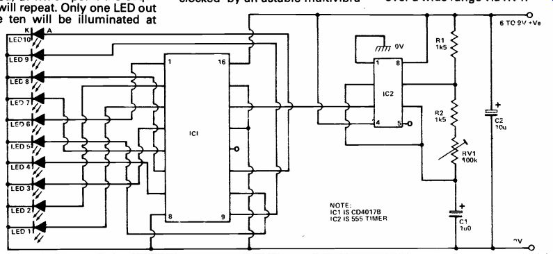
This unit produces a very attractive visual display in the form of a moving 'dot' on a column of ten LEDs. If the unit is wired up exactly as described in following paragraphs, the display will be such that an illuminated dot will appear to move sequentially and smoothly along the line of LEDs, from the bottom of the column to the top, until the top -most LED is reached, at which point the sequence will repeat. Only one LED out of the ten will be illuminated at any given moment of time.
The display can, if preferred, be wired up in a random fashion, so that the dot appears to jump about on a column of ten LEDs, but does so on a continuously repeating pattern. In either case, an attractive display will be produced. The unit can be used to simulate miniature shop display signs on model railway layouts, etc.
IC1 is a CD4017B decade counter with ten decoded outputs, and is 'clocked' by an astable multivibrator formed by IC2 and it's associated components. The action of the circuit is such that nine out of the ten decoded outputs of IC1 are low at any given moment of time, the remaining output being high.
Each time that a clock pulse arrives a different output switches high, but all outputs go high in a fixed sequence. Each output is fed directly to it's own LED, so that the LEDs also switch in a fixed sequence. The clock rate is variable over a wide range via RV1.
(adapted from: Electronics Digest (Vol. 2 No. 3--WINTER 1981))
NEXT: House and Home