Opto-Thermo Switch
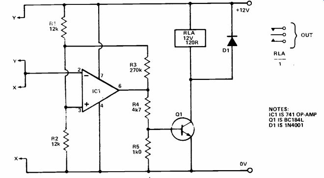
This simple but highly versatile unit has a relay output that can be activated by either optical (light) or thermal (temperature) levels.
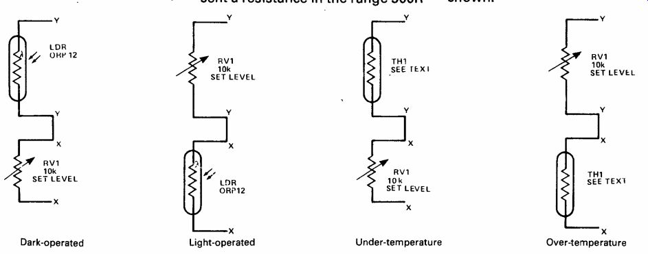
The unit can be made to activate either when these levels go above or fall below pre-set values, de pending on the manner in which the input sensors (an LDR or light-dependent resistor for photo operation, or a thermistor for thermal operation) are connected to the unit. The unit can thus function as either a 'brightness' switch, a 'darkness' switch, an over-temperature switch, or an under-temperature switch.
The unit has a multitude or practical uses. In the opto mode it can be used to automatically turn on lights when darkness falls, or to activate an alarm if a light is shone into a normally-dark area such as a cupboard or safe. In the thermo mode it can be used to turn on heating when the temperature falls below a pre-set value, or to activate a cooling system or sound an alarm when the temperature rises above a pre-set value.
IC1 is a type 741 operational amplifier that is wired as a voltage comparator. A fixed 'half supply' reference voltage is fed to input pin 3 of the op -amp via R1 and R2, and a variable voltage is fed to input pin 2 via RV1 and the LDR or thermistor. The circuit action is such that the op-amp output is normally low and Q1 and the relay are off, but the output abruptly 'switches high and drives Q1 and the relay on when the pin 2 voltage falls below the pin 3 voltage. R3 introduces a small amount of hysteresis so that the circuit switches sharply and switches at slightly different ON and OFF levels, thus eliminating relay 'chatter' problems. D1 suppresses back-emfs from the re lay coil, and this protects Q1 against damage from this source.
Connect the input sensor, either an LDR or a thermistor (and RV1) to the inputs of the unit to obtain the desired type of operation. For opto operation, the LDR must pre sent a resistance in the range 900R to 9k at the desired trigger level an ORP12 is suitable for use in most cases. For thermo operation, the thermistor must be a negative-temperature coefficient (NTC) type that presents a resistance on the range 900R to 9k at the desired trigger level: a VA1066S is suit able for use in most cases. The relay can be any 12 volt type with a coil resistance greater than 120R.
The unit must be powered from a 12 volt supply. In use RV1 is simply adjusted so that the relay just activates at the desired light or temperature level. External circuits can be controlled via the re lay contacts. Take care to connect D1, Q1, and IC1 in the polarity shown.
+++++++++++++++++
Differential Temperature Switch
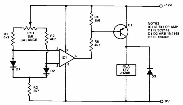
This inexpensive unit can form the basis of a number of sophisticated household -control systems. The circuit uses a couple of ordinary silicon diodes as temperature-sensing elements, and uses a relay as an output 'switch.' The circuit action is such that the relay turns on only when temperature 'A' (sensed by D1) is higher than temperature 'B' (sensed by D2), and this action occurs irrespective of the absolute value of either temperature. The circuit action can be effectively reversed, so that the relay turns on only when temperature 'A' is below that of temperature 'B', by simply trans-posting the measurement designations of D1 and D2.
Ordinary silicon diodes can develop forward voltages of several hundred millivolts at current levels of the order of 1 mA, the precise voltage value depending on the value of current and the characteristics of the individual diode that is used. All silicon diodes, however, have a virtually identical temperature coefficient of about -2mV/°C, and can thus be used as accurate temperature indicating devices.
In the circuit the two temperature-sensing diodes (D1 and D2) have currents passed through them via the RV1-R1-R2-R3 net work; RV1 allows the relative values of the two currents to be adjusted over a limited range so that the diodes produce almost identical forward voltages when they are both at the same temperature. Consequently, the differential or 'difference' voltage between the two diodes is directly proportional to the difference in their temperatures.
This difference voltage is fed to the input terminals of the IC1 operational amplifier, which is connected as a voltage comparator or differential voltage switch, and the output of the op -amp is fed to the relay via Q1. The action is such that the relay turns on when the temperature of D1 rises above that of D2.
The unit must be powered from a 12 volt supply. In use, RV1 is simply adjusted so that the relay is just off when both sensing diodes (D1 and D2) are at the same temperature. The relay should then turn on if the temperature of D1 is raised a small amount above that of D2: note that at normal room temperature this action can be checked by simply touching D1, so that body heat produces the required differential. External circuits can be controlled via the re lay contacts. The relay can be any 12 volt type with a coil resistance greater than 120R.
This switch can, for example, be used to activate a blower motor to ensure that a cellar or basement is automatically warmed by the outside air if the external air temperature is above that of the cellar or basement. Alternatively, it can be used to activate a solenoid valve to ensure that a storage tank is automatically filled only from the hotter of two alternative water sources, etc.
+++++++++++++++++
Combination Lock
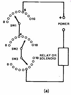
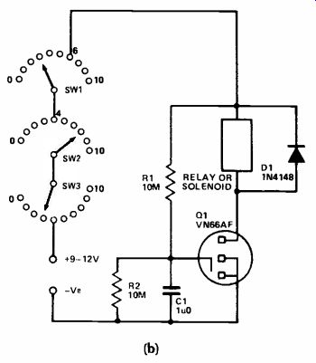
Most combination locks are based on the simple arrangement shown in (a). This merely consists of three ten way rotary switches wired in such a way that they will connect power to the relay or sole noid if the correct combination is set ( 6-4-5 in this case). This basic circuit is not often used in practice since it does not take very long to quickly adjust the switches through all the 1,000 possible combinations (0-0-0 to 9-9-9 inclusive) if it is done in a logical manner.
One of the simplest and best methods of overcoming this problem is simply to build a delay circuit into the unit so that power is not supplied to the solenoid or re lay until the correct combination has been present for a few seconds. Quickly running through all the possible combinations is then ineffective at "cracking" the unit, as the delay circuit will prevent the unit from responding when the correct combination is briefly present. Anyone trying to "crack" the unit is very unlikely to succeed unless they know of the delay circuit and are prepared to devote a good deal of time to finding the correct combination.
Circuit (b) has an additional time delay circuit which is based on VMOS device Q1. When the correct combination is set on SW1 to SW3 and power is supplied to the circuit, C1 will be uncharged, giving zero gate bias to Q1. Q1 is, therefore, switched off and no significant current is supplied to the relay or solenoid which forms its drain load. C1 slowly charges via R1 and after about 4 s the voltage on C1 will be large enough to bias Q1 into conduction and switch on the relay or solenoid.
R2 discharges C1 when the unit is reset, so that it is quickly ready to operate properly once again. R2 limits the maximum gate voltage of Q1 to about half the supply voltage, but this is more than adequate to bias the device hard into conduction and is of no practical consequence. D1 suppresses the high back emf produced across the relay or solenoid when it switches off and prevents possible damage to Q1.
++++++++++++++++++
Touch-Switch
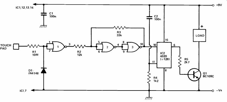
This touch switch is designed to provide on/off switching for 9 volt battery operated equipment having a current consumption of up to 100mA. It has a single contact which is briefly touched in order to change from on to off or vice versa. The circuit is operated by stray pick-up of mains hum which is coupled to the input of gate 1 (which, like the other three gates employed in the unit, is connected to act as an inverter) via R1 when the input contact is touched. As IC1 is a CMOS device it has a very high input impedance, and the in put signal will be capable of switching gate 1 input from one logic state to the other. The input impedance of the circuit is so high that the reverse resistance of D1 is used to tie the input to earth under quiescent conditions, so as to prevent spurious operation. R1 acts as a low pass filter in conjunction with the input capacitance of the circuit, and this attenuates high frequency noise which may be present on the 50Hz mains signal.
The output from gate 1 still contains significant noise products, and also has a rise time which is inadequate to drive the final stage of the circuit. This is overcome by using the trigger circuit based on gates 2 and 3. R3 tends to hold gate 2 input in the same state as gate 3 output, resisting any change in logic state caused by gate 1 output due to the coupling through R2. R2 has a lower value than R3, and so gate 1 can operate the trigger circuit if its output signal is of adequate amplitude. The main 50Hz signal will be strong enough, but the noise spikes will not, and are thus eliminated from the output of the trigger. Once the output of the trigger starts to change state, the coupling through R3 ensures a rapid change.
IC2 is a 14 stage binary (divide by 2) counter, and Q1 is driven from the output of the seventh stage via current limit resistor R5.
C2 and R4 provide a positive reset pulse to the counter at switch on so that the outputs are low, and Q1 is switched off. The controlled equipment forms the load for Q1, and obviously receives no significant power. If the touch contact is operated, a 50Hz signal is fed to IC2 and the 7th stage output changes state every 64 pulses. As this output goes high and low the load is switched on and off. In practice the contact is touched just until the unit switches to the desired state (which one tends to do automatically).
The unit consumes about 1uA in the "off" mode and approximately 3mA in the "on" state.
+++++++++++++++++
Light Sensitive Switch

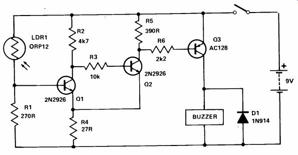
Light dependent resistor LDR1, type ORP12, has the property of having a very high resistance in complete darkness (over 1MR), but in the brightest light this falls to nearly 300R (although individual devices vary greatly).
For simplicity the circuit will be described for 'dark on'.
When daylight is falling on the ORP12 the resistance is fairly low - the actual value is not important but it will be in the range of 300R to 3kR. With R1, the two components form a potential divider with the base of Q1 connected to the junction; Q1 is biased on, Q2 is held off and, following the chain of R5 and R6, it will be seen that the base of Q3 is connected to the positive supply, and is therefore non -conducting.
As the light on ORP12 de creases, the voltage at Q1 base falls; the current through Q1 fails, the voltage across it increases, and this starts to bias Q2 into conduction.
As Q1 and Q2 share the same emitter resistor there is a regenerative action. Q2, by becoming conductive, raises the voltage on the emitter side of R4 and, since the base voltage on Q1 is still at the same level, this biases Q1 even more into non -conduction.
The switching action is extremely rapid once it has started and the effect is that, although the voltage at the base of Q1 is changing gradually, Q2 is switched completely on at a certain point, and Q1 is switched off.
When Q2 is switched on, the voltage at the collector falls and Q3 is biased into full conduction through R6. With Q3 on, current is passed through the buzzer.
A relay can be used in place of the buzzer--its coil resistance hardly matters - however, relay coils should always be by-passed with a diode.
A 'dark off' (or 'light on') circuit can be made by reversing ORP12 and R1 - which now becomes 33k. In this condition Q1 is on but as the light level increases the voltage at the base of Q1 falls and the same action applies as before.
In both versions of the circuit R1 can be replaced by a variable resistor and this enables the light level at which the circuit triggers to be varied.
Note that Q1 and Q2 are silicon N-P-N types whereas Q3 is germanium P-N-P type. Q3 passes quite a large amount of current and can be destroyed unless a heat sink is used - one of the fin types which clip over the body should be adequate.
When Q3 is off the current consumption is very low--about 4mA.
(adapted from: Electronics Digest (Vol. 2 No. 3--WINTER 1981))
NEXT: Sequence and Timing