Tracking filters demodulate two audio-band fm signals
by Stephen Barnes Center for Bioengineering, University of Washington, Seattle
Because of the way in which they retrieve recorded data, many systems designed for monitoring biomedical functions have to demodulate two closely spaced fm carrier signals in the audio-frequency band. The original data signals could be recovered with low-pass filters, but they are an expensive solution since their cutoff must be sharp to prevent cross modulation, signal blocking, or undue limiting of the bandwidth needed by one or both signals.
The low-cost solution shown here, however, uses a dividing phase-locked loop to demodulate one signal and to provide the clock signal for a tracking notch filter that recovers the other channel of data.
The advantages of the circuit may be seen for a typical monitoring case in which a 30-hertz electrocardiogram signal (having a frequency too low to be recorded directly on cassette tape) is placed on a 9-kilohertz carrier.
This signal is applied to the LF356 amplifier along with a 0-to-6-kHz signal from an ultrasonic Doppler flowmeter that provides data on blood circulation.
Block A, the dividing phase-locked loop module, oscillates at a free-running frequency equal to 8fm. It is here that the 9-kHz carrier is directly demodulated. Also included in block A is a 74C193 divide-by-8 counter in the PLL's feedback loop, which provides the driving signals for the CD4051 multiplexer in block B. This block contains the sampling filter which passes frequencies equal to 1/8 the sampling frequency, 8fm, and its harmonics. Thus the Doppler Ota is notched out by the sampling filter. But signal _Jm is subtracted from the original input signal f0+ fm by the differential amplifier in block C. Therefore, only signal fc, will appear at the output.
Resistor RQ, which is in the PLL's feedback loop, controls the width of the notch, which is given by B =I /81r RQCQ, where B is the width defined by the filter's upper 3-decibel frequency minus its lower 3-dB frequency. Potentiometer R5 is used for balancing the differential amplifier by nulling the 9-kHz feedthrough signal.
When the circuit is in the locked state, the minimum attenuation of the fm signal will be approximately 33 dB for input signals ranging from 540 millivolts to 8 volts peak to peak. Below signal levels of 540 my, feedthrough from the multiplexer will reduce the attenuation.
Because the filter is a sampling device, it is subject to aliasing if any input-frequency components approach the Nyquist limit of 4fm, so that precautions should be taken to prevent this. Spurious output components that are higher harmonics of the 9-kHz fm signal or the clock signal can be removed easily.
Phase jitter in the PLL should also be minimized, for it causes narrow noise sidebands centered about the 9-kHz fm signal and separated from it by a frequency equal to the loop bandwidth of the PLL. The amplitude of these noise sidebands in a properly adjusted circuit should be down at least 33 dB from the level of the fm signals at the input.

--------- Recovery. Blood-flow information contained
in Doppler signals in 0-to-6-kHz audio band and fm carrier bearing electrocardiogram
data are efficiently separated without the need for conventional low-pass
filters. Phase-locked loop recovers EKG data directly, while providing
the clock signal for the sampling notch filter in block B that eliminates
fm carrier but passes the doppler signal.
Voltage-controlled integrator sets filter's bandwidth
by Henrique Sarmento Malvar Department of Electrical Engineering, University of Brazilia, Brazil
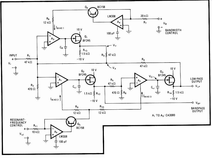
Because it uses operational transconductance amplifiers as electrically tuned integrators for selecting a state-variable filter's center frequency and bandwidth virtually independently of one another, this circuit is ideal for use in music and speech synthesizers that require individual voltage-controlled setting of these parameters.
As shown, input signals to be processed are applied to transconductance amplifier A1, whose bias current is derived from voltage-to-current driver AsQ5. The bias current, in turn, is set by control voltage V, which ultimately determines the filter's center frequency. In general, Ibias = V./2R, .
Placing the capacitor C across the output of the operational transconductance amplifiers A1 and A2 converts the two-stage network into a noninverting integrator, the transfer function becoming Vo(s)/V,(s) = k/s, where k is the 3080's transconductance factor k' /C, and transconductance k' as given in its data sheets is k' = 19.2 Ib..s. Substituting for It., Vo(s)/V,(s) = 19.2 V,/sRC,.
Placing integrator A3 in the feedback loop of A1 and A2 equips the basic filter with the capability to control bandwidth. As seen from inspection of the circuit:

where the low-pass function is given by:
VLp(s) =- (k2/s)2Vx(s)R6/(R5 + R6) and where Vy(s) =- kIVK(s)/s.
Constants kl and k2 are given by:
ki = 19.2 VB/R7CB k2 = 19.2 and the bandpass function, VBP(s), equals- k2Vx(s)/s.
Assuming R1 = R3 = R4 = R5 = R' and R2 = R6
= R", with R"/R' = a«1, it follows that
= R2. Substituting the appropriate quanti ties back into all the above equations, it is seen that:
VLp(s)/V,(s) =- 1/[(sice.)2+ (B/coo)(s/w0)+ 1] VBp(s)/V,(s) =- (s/coo)/(s/w0)2+ (B/(.00)(s/wa) + 1] where the resonant frequency and the bandwidth are given by:
coc,(rad/s) = ak2 =
B(rad/s) = aki = 19.2aVB/R7CB Parameter a should be near 0.01, to ensure the best compromise between distortion and signal-to-noise ratio.
The bias current of the operational transconductance amplifier should not be more than 500 microamperes.

---- State-controlled. Placing a voltage-controlled operational-transconductance-amplifier
integrator in feedback loop of similarly wired stages lets state-variable
filter set center frequency and bandwidth electrically. Bandwidth and
frequency settings are virtually independent of one another. The circuit
thus becomes extremely attractive for music and speech synthesis applications.
Inverting amplifier flips filter's response curve
by Henrique Sarmento Malvar Department of Electrical Engineering, University of Brazilia, Brazil
The voltage-controlled bandpass filter so popular in music synthesizers and useful in remote-tuned receivers can be also made to work in the band-reject mode by placing an inverting operational amplifier stage in the existing filter's input/output feedback loop. In that way, a controlled notch, which is often equally valuable in the aforementioned applications, may be put together at low cost.
The transfer function of the typical VCF is given by:

where wo is the voltage-controlled resonant frequency and k is the damping factor, which is usually adjusted with a potentiometer. It is seen that when k is at its maximum, the response approaches that of a wideband filter. As k decreases, the filter's Q increases, and the bandwidth therefore decreases. At the limit, for a value of k that is slightly negative, the system oscillates at By adding the operational amplifier and its gain-controlling resistors to the feedback loop of the VCF as shown in (a), the output voltage generated is:
Vo(s) =- Vo(s)H(s)- V,(s)
This expression leads to the transfer function:

This function has two zeros and two correspondingly equal poles. But although the absolute value of both pairs is the same, for k>.-0.25 the poles will be more damped than the zeros, and thus the filter's frequency response will be mainly determined by the zeros. There fore, the system will operate as a band-reject filter (b).
The deepest null is attained at k = 0, and a theoretically infinite attenuation is thereby achieved at w = w_o.
Thus the filter can be tuned to null the fundamental frequency of any synthesized signal, leaving only its harmonics. If the frequency control is simultaneously fed with a low-frequency sine or triangle wave, the so-called phaser sound used for special effects is obtained.
As k is increased toward infinity, the null becomes less sharp and the filter offers almost no attenuation at any frequency, thereby behaving as a quasi-all-pass network.
Note that as k increases beyond k = 10, the filter response approaches that of k =-0.25. Clearly, k should not be less than- 0.25, because the poles of the function will again become prominent and the system will once more behave as a bandpass filter. At k <- 0.50, the system will oscillate.

--------- Double duty. Adding inverting op-amp stage into feedback
loop of music synthesizer voltage-controlled bandpass filter (a) adapts
it for band-rejection duties. Notch depth (b), selected by filter's damping
potentiometer, may be adjusted for a maximum value of-60 dB.
Logic-gate filter handles digital signals
by Andrzej M. Cisek Electronics for Medicine, Honeywell Inc., Pleasantville, N. Y.
Performing the digital counterpart of electric-wave filtering in the analog domain, this unit can function as a low-pass, high-pass, bandpass, or band-reject filter of a square-wave pulse train. No RC integrating networks or comparators are needed, the all-digital filter being tuned simply by adjusting the reference frequency. Built originally for biomedical applications, it can find much broader use in the field of communications.
Consider the case of the band-reject filter shown in (a) in the figure. As seen with the aid of the timing diagram, the Q output of the edge-triggered set-reset flip-flop formed by the gates of the CD4011, A1-A4, and the 4013 D flip-flop (B1) is brought high by the training edge of reference frequency fo and brought low by the falling edge of signal fl. The combined output of the flip-flop and fo appears at gate C1, moving low if fo>f1.
Similarly, C2 moves low if f1>f0. Therefore, signals from the output of the NAND gate formed by NOR gates D1-D4 appear whenever fo # fi. Each pulse sets flip-flop B2 high if it is not already so, permitting signal fi to pass through to the output.
Meanwhile, the 12-stage 4040 ripple counter advances on each pulse from fo. The counter will reach the Q, state if fo = f,, because no reset pulse can emanate from gate D4 under that condition. These events will disable gate C3 and prevent fi from reaching the output.
The steepness of the filter's roll-off characteristic will be determined by which stage of the counter resets flip-flop B2. The filter's reaction time to changes in the input and reference frequencies will vary accordingly that is, the steeper the slope, the longer the response time, this delay being the major drawback of the filter.
The corner frequencies are f, min = (N- 1)fo/N and f, max = (N +1)fo/N, where N is the number of pulses of fo required for the counter to produce a reset pulse. The quality factor is Q = fo/Aft = N/2.

-------- Digital damping. To perform band-reject function, this combinational
logic circuit ascertains the frequency relationship of two square-wave
signals. Tuning is done by adjusting the reference frequency. Selectivity
is determined by tap position On of the counter. Waveforms for given
points in circuit show timing relationships. With minor changes, the
filter is easily adapted for high-pass, low-pass, and bandpass duties.
The stop-band filter can be easily modified to a band pass type if the Q output of flip-flop B2 is wired to serve as the inhibit line. To convert the filter for low-pass duties C2 is removed and both inputs of D3 are connected to DI. In like fashion, C1 is removed and both inputs of
D3 are connected to D2 if a high-pass response is desired.
Note that the NOR-gate circuitry is required to avoid any ambiguity of output state when pulses of input and reference signals overlap. Also, resistors R1 and R2 neutralize the effect of variable propagation-time differences of fo and fl through the gates
Low-pass Chebyshev filters use standard-value capacitors
by Ed Wetherhold Honeywell Inc., Signal Analysis Center, Annapolis, Md.
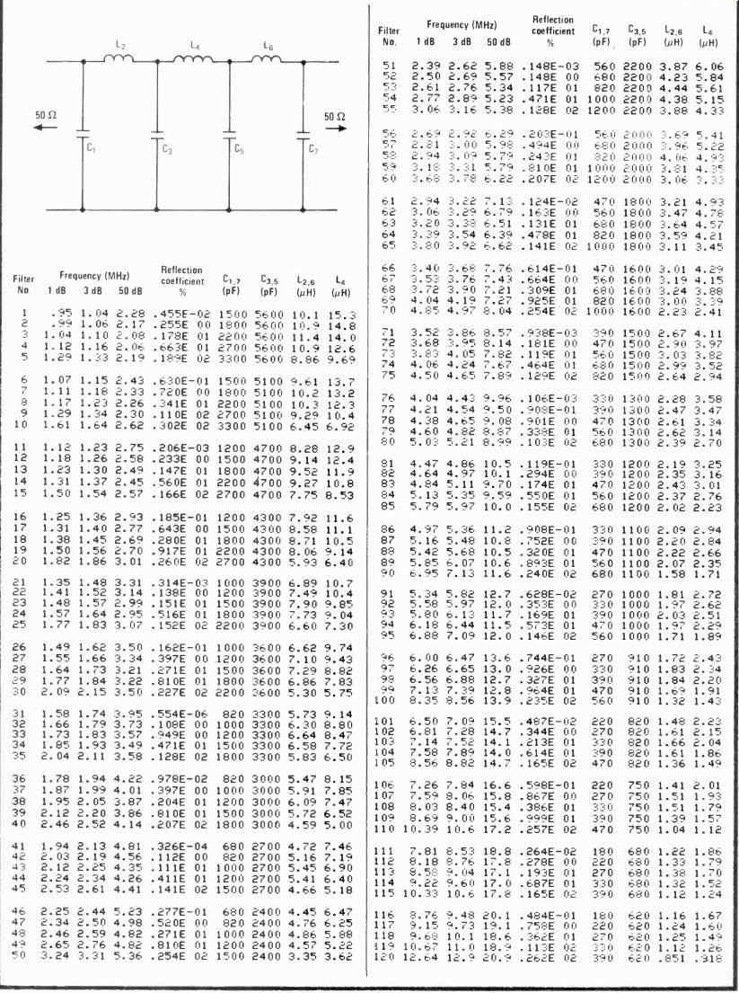
If a low-pass filtering requirement is such that a roll-off attenuation of 40 decibels per octave is adequate, this table will enable rapid design of seven-element filters of the Chebyshev variety using standard-value capacitors.
Both L and C values are given directly for operation in the 1-to-10-megahertz region and are scaled for frequencies outside this range. Element values, specified for filters having a source and load impedance of 50 ohms, are easily calculated for any impedance.
Component values for the Chebyshev filter (see table), which is characterized by low-level equi-ripple response throughout its passband, have been derived by an 85-line program written in Basic. In this configuration and for the equally terminated case, C1 = C7, C3 = C5 and L2 = L6. Once a standard-capacitor value for C3/C5 is specified, capacitors C1/C7 and inductors L2, L4, and L6 are found for a given reflection coefficient selected to ensure that C1 is also a standard value. The frequencies corresponding to the 1-, 3-, and 50-dB attenuation points are also calculated.
A simple example illustrates the use of the table.
Consider the case of a filter whose 3-dB cutoff frequency, Ff, is 6 megahertz and whose terminating impedance, Zx, is 75 ohms. The user must:
Find the scaled impedance factor R = Zx/50.
Calculate the 3-dB cutoff frequency of the 5042 filter from FP = RF;, dividing Zx by 10^ where n = 1, 2, . . . if necessary to ensure FP < 10 wiz.
From the table, select the design closest to that meeting the calculated FP requirement. Note the tabulated values of C will be used directly in this design, and the L values will be scaled.
Calculate the exact value of F; = F,"°/R, where gs° is the tabulated value.
Calculate the new L2/L6 and L4 values for the given terminating impedance from L = R2Lso.
Given FIL = 6.0 wiz and Zx = 75 S2, it is seen that R = 75/50 = 1.5, R2 = 2.25 and FP = 1.5(6) wiz = 9.0 MHz. Filter number 109 is selected because its FP value is closest to the desired specified value. Thus C1,7 = 390 pF, and C3,5 = 750 pF. Inductors L2,6 = R2(1.39) = 3.13 microhenries; L4 = R2(1.57) = 3.53 µH. These components may be conveniently hand-wound on standard toroidal cores that are readily available. Note that design 109 has a reflection coefficient of 9.99%. If the filter must be operated at a low voltage standing-wave ratio, then design 113, which has a reflection coefficient of only 1.93%, should be used.

---------- DESIGN TABLE: LOW PASS CHEBVSHEV FILTERS
High-pass Chebyshev filters use standard-value capacitors
by Ed Wetherhold Honeywell Inc., Signal Analysis Center, Annapolis, Md.
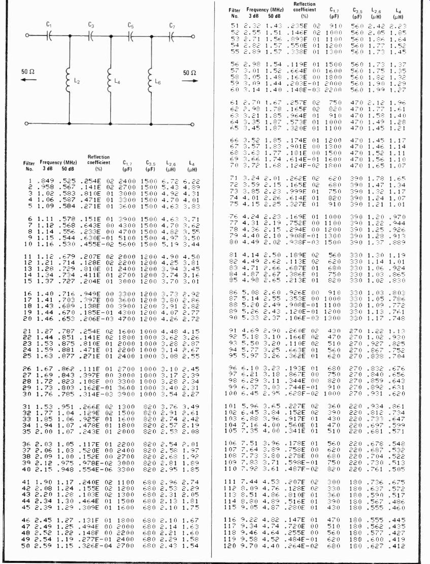
Complementing the computer-generated design table for low-pass Chebyshev networks having standard-value capacitors [Electronics, June 19, 1980, p. 160], this listing is useful for building seven-element filters of the high-pass type that provide a roll-off attenuation of at least 42 decibels per octave. Both L and C values for 120 filters were found by an 85-line program written in Basic and were tabulated for an operating range of 1 to 10 megahertz. These components can be scaled for frequencies outside this range. Element values are specified for a source and load impedance of 50 ohms, but values for any input/output impedance are easily determined.
The high-pass filter (see table) uses a capacitive input and output configuration to minimize the number of inductors and to provide dc isolation with respect to ground. In this configuration and for the equally terminated condition, C1 = C7, C3 = C5, and L2 = L6. Given a standard capacitor value for C3 and C5, the program calculates all capacitor and inductor values for those unique values of the reflection coefficient that make C1 and C7 a standard value. The frequencies corresponding to the 3- and 50-dB attenuation levels are also listed.
To scale the tabulated frequency and component values into the 10-to-100- or 100-to-1,000-mHz frequency range decades, the user must multiply the frequency by 10 or 100, respectively, and divide all C and L values by the same number. Similarly, for the 1-to-10-, 10-to-100- and 100-to-1,000-kilohertz decades, the frequency is divided by 1,000, 100 or 10, respectively, and the component values are multiplied by the same number.
The following example demonstrates how to design for an vo impedance other than 50 Ohm. Consider a filter having a terminating impedance, Zx, of 75 SZ and a 3-dB cutoff frequency, FIL, of 9.4 MHz. The user must:
Calculate the impedance scaling factor, R = Zx/50.
Calculate the 3-dB cutoff frequency of a 50-12 filter, Fr, from Fr = RF;. If Fr is found to exceed 10, the table is scaled into the next frequency decade.
Select the 5042 design from the table that most closely matches the calculated Fr value. The tabulated capacitor values are implemented directly in the new design.
Find the new inductor values by multiplying the corresponding tabulated values by the square of the impedance-scaling factor, R.
Find the corresponding 3- and 50-dB attenuation points by dividing the tabulated frequencies by the impedance-scaling factor.
Thus, for an F; of 9.4 MHz and a Zx of 75 S2, R = 75/50 = 1.5, R2 = 2.25, and Fr = 1.5(9.4) = 14.1 MHz. Because Fr is greater than 10 MHZ, the 50-f/ tabulation is scaled to the 10-to-100-MHz decade by multiplying all frequencies by 10 and dividing all component values by 10. The user should select filter number 17 because its Fr value is closest to 14.1 MHz.
Therefore, C1,7 = 360 picofarads, and C3,5 = 120 pF.
Inductor L2,6 = R2(0.380) = 0.855 microhenry, and L4 = R2(0.286) = 0.644 Further, FP = 14.1/1.5 = 9.4 MHz and Eig = 4.69 MHz.
To construct the filter, polystyrene capacitors with a 2.5% tolerance, such as Mallory type sxm, are suitable. The inductors may be conveniently hand-wound on standard powdered-iron toroidal cores.

---------- DESIGN TABLE HIGH-PASS CHEBYSHEV FILTERS
[source: ISBN 0-07-606808-0 Copyright© 1982 by McGraw-Hill, Inc. ]