Dynamic logic probe displays five states
by Mihai Antonescu
Federal Institute of Technology, Lausanne, Switzerland Providing the convenience of the logic probe proposed by Prasad and Muralidharan, which utilizes a seven-segment display readout rather than discrete LEDs or lamps, this five-state detector also senses the presence of pulses and differentiates between the logic 0 and open-circuit conditions. Furthermore, provision has been made to bias the probe via its external-reference inputs, permitting it to check logic levels in circuits built with either TTL or complimentary-MOS devices.
As shown in the figure, the test signal, Vin, is compared with reference voltages Vref1 to Vref4 at comparators A, to A3. Voltages Vref1 to Vref2 are derived from the supply that powers the circuit under test, with Vref3 (developed from the probe's power source) and Vref4 at approximately 0.05 volt and 0.1 v below ground, respectively. Switches S1a and S1b at the voltage divider are used to set the required logic-level references at A1 and A2 in order to check either TTL or C-MOS circuits.
Gates G1-G13, comprising the combinational-logic detector, determine Ws relation to Vrefi-Vf4 and activate the appropriate segments of the display (see table).
A1 and A2 are used to check for the logic 1, 0, and guard-band conditions. A3 is used to detect the no-connection, or open-circuit, condition, which can be differentiated from the logic 0 state because Kept is maintained at 0.1 v below ground. Note that the logic 0 state for TTL will typically be 0.4 V and is hardly ever below 0.2 v, whereas the logic 0 state for c-mos will be typically 0.01 V.
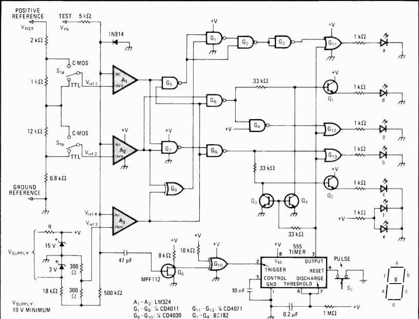
-------- All-state. Logic probe having seven-segment display detects
logic 1 and guard-band conditions, can differentiate between logic 0
state and open circuit, and senses a pulse train. Unit can check logic
levels in circuits built with the two most popular families, C-MOS and
TTL.
Switch S2 must be depressed to catch any expected input pulses having a width down to 15 nanoseconds.
This action resets the 555 one-shot, enabling it to over ride the displayed symbol with the letter P when the pulse arrives. If a train of pulses having a repetition rate greater than about 0.2 seconds (the time constant of the 555) is detected, the P will be displayed indefinitely.
With faster one-shots, pulses of 5 ns can be snared.
The probe can be powered by any dc source having a minimum voltage of 19 v. Resistor R should be selected to pass about 30 MA to the probe circuit.

----- RESPONSE OF FIVE-STATE LOGIC PROBE
Referencing
1. S. Jayasimha Prasad and M. R. Muralidharan, "Logic tester has unambiguous display," Electronics, March 3, 1977, p. 117.
Digital comparator saves demultiplexing hardware
by V. L. Patil and Rahul Varma Central Electronics Engineering Research Institute, Pilan. India
Comparing two m-digit numbers, where each digitcom prises n bits, by conventional means requires the services of a demultiplexer for separating the data into two corresponding sets, 2mn storage elements that convert the data into bit-parallel, digit-parallel form, and m magnitude comparators for performing the actual comparison. The demultiplexing can be simplified, however, and the number of storage elements reduced to 3m with this technique, which utilizes strobed memory elements in the form of D flip-flops and combinational logic to ascertain the relationship of the two numbers.
The method is illustrated for an example where two 4-bit, 3-digit numbers are compared. As seen, the corresponding digits of both numbers are simultaneously introduced to the 7485 4-bit comparator, Ao, with the least significant bits being introduced first. The result of the comparison is then strobed into the 7475 quad latch, A1, by digit strobe D.
Similarly, the second-most significant bits (ssa) and the most significant bits are then strobed into A2 and A3, respectively, by strobes D2 and D3. The combinational logic that follows then evaluates the three-digit (MsD, SSD, and LSD) comparison from:
OL = L3+ E3L2+ E3E2L1
OG = G3+E3G2+ E3E2G1
OE = E3E2E1
where OL = 1, OE = 1, and OG = 1 signify that A < B, A = B and A > B, respectively, and L1, E1, and G1 are the individual corresponding outputs of flip-flops A,.
The truth table outlines circuit operation.
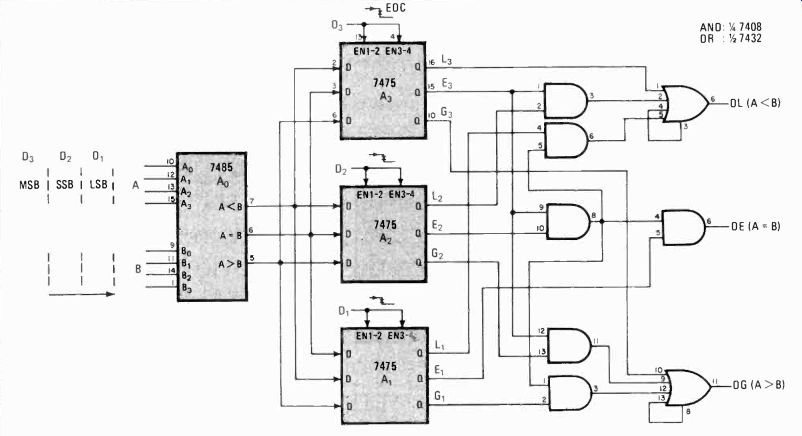

-------- Reduction. Circuit performs n-bit, m-digit
comparison of two numbers without a conventional IC demultiplexer, reduces
number of memory elements normally required. Simplified decoding technique
utilizes combinational logic. Truth table outlines circuit operation
in comparing most, second-most, and least significant digits.
Digital comparator minimizes serial decoding circuitry
by Harland Harrison Memorex Inc., Communications Division, Cupertino, Calif.
Using significantly fewer chips than the comparator proposed by Patil and Varma', this two-word, 4-bit comparator offers other advantages as well-it accommodates any word length and is more easily modified to handle any bit width. The control signals needed to facilitate the comparison can also be more conveniently applied.
The circuit outputs are first cleared with a negative-going pulse from the start signal. This sets outputs O_LESS and O_GREATER low. O_EQUAL, derived from O_LESS and O_GREATER, goes temporarily high. At this time, the numbers can be presented to data buses A and B for comparison, with the least significant bit pair introduced first. As a consequence of the configuration, any number of bit pairs per word can be compared without modifying the circuit at all. The data buses each accept up to 4 bits, but this number may be expanded simply by cascading 7485 comparators.
The result of each bit-pair comparison is then latched into the 7474 flip-flops by the D1 clock pulse, with the results of each bit-test being fed to the cascade inputs of the 7485. As a result, the comparator keeps track of the previous bit-pair check while continuing to update its results as each succeeding bit pair is introduced. Thus the need for additional memory and logic elements is eliminated. The final result becomes valid after the D clock pulse, where m is the word length in bits, and remains valid until the next start pulse.
References
1. V. L. Pahl and R. Varma, "Digital comparator saves demultiplexing hardware," Electronics, Aug. 14, 1980, p. 129.
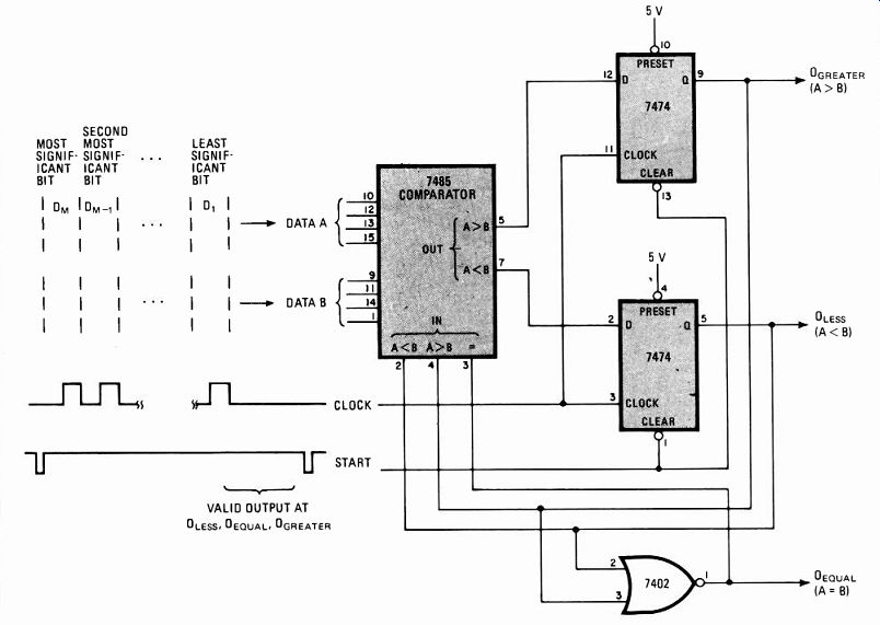
-------------- Less memory. Circuit performs 4-bit
comparison of two numbers with minimal circuitry. 7485 comparator replaces
large numbers of flip-flop-type memories and logic elements by keeping
track of previous bit-pair checks in real time as each pair is introduced.
Circuit accommodates any word length; bit width is expandable simply
by cascading 7485 comparators.
Dual one-shot keeps firmware on track
by Patrick L. McLaughlin, Teletech LaGuardia Inc., R&D Labs, Lafayette, Colo.
By noting the absence of pulses generated by status reporting statements inserted in a running program, this missing-pulse detector reinitializes a microprocessor-based system when glitches on the power line or peripheral circuitry occur. The circuit provides more efficient system performance than a periodic reset timer and is much less expensive than installing line filters or isolators. Only one chip is required-a dual re-triggerable monostable multivibrator.
Problems created by a power glitch-such as shuffling of information in the data registers and program jumps to undefined locations or to a location that gives rise to infinite loops-are conventionally solved by placing a timer in the system's reset line to initialize the system every 15 minutes or by using a brute-force power-line filter or even a dynamotor power isolator. A timer probably offers the best low-cost solution, but system speed is degraded by the unnecessary periodic interruptions.
A better solution is to provide a way for the program to report to the system hardware that it is running and on track. Using the 74123 dual one-shot, as shown in the figure, to monitor so-called report statements that are entered in the program's housekeeping loop automatically resets the microprocessor if and when the reports stop for longer than a specified period.

--------- Restart. 74123 dual one-shot, configured
as missing-pulse detector and output timer, detects absence of program
report statements caused by power-line glitches in order to efficiently
reinitialize microprocessor. Reports are entered as often as required
in wait-for-data-type systems to ensure pulse rate falls within t window.
Circuit accommodates static-type stop typical 8080/8085 wait instructions.
In general operation, both one-shots (one serving as the missing-pulse detector, the other as the output timer) trigger each other alternately in an astable, free-running mode, with RIC, setting the report window, tw, and R2 setting the reset time, ti. On power up, pin 12 of the 74123 is low and the processor is kept at rest until both one-shots time out. Then pin 12 is brought high, enabling the processor. If no report is made before time t, the cycle is repeated. An active-low series of report pulses made any time before tw resets the missing-pulse detector (the output is Q1), keeping pin 12 high and the processor running.
Usually, report statements are routinely entered before, after, or at both ends of the program's house keeping loop and in most cases will be called frequently enough to fall within the t. time window. In loops that may delay normal reporting, however, such as wait-for-data types, inclusion of additional report statements is advisable.
Note that if pin 11 is brought to ground, the one-shot at the output will be inhibited without resetting the processor. Thus, this circuit can accommodate static-type stops typical of the 8080/8085 wait instruction and is usable with slow-running programs and single-stepping arrangements.
The 74123 can be rewired to accept positive-going report pulses simply by introducing the report line to pin 1 of the chip and making pin 5 the output reset line. Pin 3 is then connected to 5 volts and pin 10 disconnected from the positive supply and connected to pin 4 instead. Finally, pin 2 is connected to pin 12.
Index separator extracts all disk formats
by David L. Jaffe Veterans Administration Medical Center, Palo Alto, Calif.
This circuit allows a soft-sectored disk controller to handle data in both hard- and soft-sectored formats. It does this by detecting the index-hole information that is sent in both formats for proper information processing. Thus, a hard-sectored disk may be used to store soft-sectored data.
As seen, the 74121 one-shot accepts all sector and index pulses that are generated-32 sector-hole pulses and one index hole in the hard format and only one index hole in the soft format. The one-shot standardizes each input pulse to a width of 480 microseconds.
The 74122 one-shot that follows is configured to pass pulses whose falling edges are displaced more than 3.56 milliseconds apart. No index pulse from a hard-sectored disk appears at this output because the time between the last sector pulse and the index pulse is only 2.55 ms. Missing index pulses are restored by the NAND gate, however, and appear at G1 (point 1).
The signal is then introduced into the last 74122 one-shot, which works as a re-triggerable monostable multivibrator with a time of 200 ms. Because index pulses occur once per revolution (166.66 ms), its Q output will remain low. Then, point 2 remains high. If a soft-sectored format is used, point 1 will be high and G2 will pass those pulses. Thus, independent of the format used, index pulses will appear at G3 (point 3).
The circuit can be connected between daisy-chained disk drives and the disk controller. This circuit can serve all drives in the chain because only the selected drive's index pulses are exerted on the index line leading to the controller.
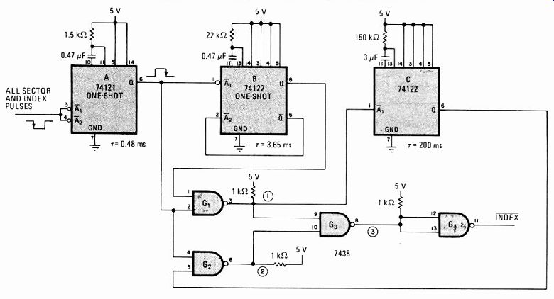
Capture. The circuit above separates index pulses from sector-hole output
of hard-disk format and detects single index pulse for soft disks, so
that both formats can be handled by one disk controller. As a result,
a hard-sectored disk can store soft-sectored data.
Dual-feedback amplifier zeros comparator hysteresis
by Svein Olsen Royal Institute of Technology. Stockholm, Sweden
Amplifiers with positive feedback may be combined to create voltage comparators and zero-crossing detectors devoid of hysteresis. Alternatively, the amount of hysteresis, either positive or negative, may be selected. In both cases, feedback ensures that true bistable (switching) operation is achieved without undue sacrifice of noise immunity- a necessary condition for optimum comparator and zero-detector performance.
The ideal voltage comparator cannot be realized with a single amplifier because bistable operation does not occur until hysteresis starts. Witness today's typical comparator--a fast differential amp and a transistor-switch output stage that actually operates as a linear amplifier within a small region about the transition level.
Achieving a step transition for slowly varying input signals is difficult with these high-gain, wideband devices, too, because of the radio-frequency oscillations and multiple transitions that occur in association with very small noise signals.
Introducing positive feedback to increase loop gain and thus ensure bistable operation, as some have tried, will yield clean switching independent of input slope. But hysteresis also is introduced, and, worst of all, At, a varying input/output delay--which depends on the slope of the input signal and the instantaneous value of hysteresis--comes into play.
The block diagram (a) shows how to achieve bistable operation while eliminating all of these problems. Amplifiers 1 and 2, each having positive feedback (a, respectively), are applied to their individual summing junctions, where they are combined with the input signal. Amplifier 1 also drives the second summing junction with a dc-level shift signal (f k) that is a function of the amp's hysteresis. Note that this feedback signal can be derived by either a switching or a linear stage.
Depending upon its polarity, the signal may add to or subtract from the amount of hysteresis inherent in amplifier 2. In the special case, total circuit hysteresis may be eliminated with little loss of noise immunity. At the same time, the circuit will retain high gain for true bistable operation. (The lengthy mathematical analysis of the circuit may be found elsewhere.') A practical circuit having Tit-compatible outputs is shown in (b). Feedback in both amplifiers is determined by resistors r and R. In this application, r is 150 ohms and R is 15 kilohms, so that VHI = 40 millivolts (Vix nix = 15 my root mean square) and Vx = 20 my, where VH1 is the hysteresis for amplifier 1 and V, is the noise immunity.
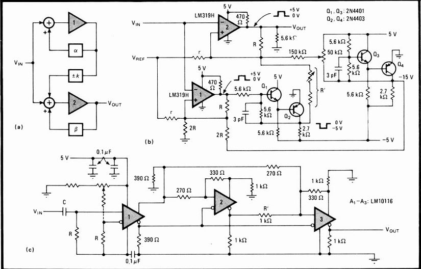
--------- Ideal. Amplifiers with high loop gain
work as nearly perfect comparators and zero-crossing detectors when they
are suitably combined to cancel hysteresis (a). The implementation of
a practical comparator (b) and a zero-crossing element (c) are relatively
simple.
Amplifier Q1-Q2 provides an inverted feedback signal to the second summing junction, with the magnitude of the signal set by potentiometer R'. The negative voltage at the junction of amplifier 1 required to establish a level-shift voltage at amplifier 2 is provided by Q3-Q4.
The output hysteresis is adjustable to zero.
A fast (3-nanosecond) zero-crossing detector with zero hysteresis is shown in (c). This application requires an LM10116 emitter-coupled-logic receiver to be used, and although its low amplification factor makes it a little more difficult to achieve high loop gain, three sections are used to make up for the shortcoming.
Amplifier 1 is the input stage biased for Class A amplification. The input RC values are selected according to the impedance-matching requirements and to provide the required low-frequency response. Amplifiers 2 and 3 serve the functions previously mentioned.
References:
1. Svein Olsen, "The Zero Hysteresis Comparator," RVK-78 Conference Notes, Stockholm. March 29, 1978.
Decoder logs signals' order of arrival
by Claude Haridge Ottawa, Ontario, Canada
This decoder indicates the sequence of arrival of up to four digital input signals and therefore serves as an excellent priority encoder. Alternatively, it can aid the technician in troubleshooting high-speed circuits. Using Schottky TTL devices to minimize propagation delays, the decoder can resolve two signals only 30 nanoseconds apart.
As shown, one flip-flop, three NAND gates, and four light-emitting diodes per input are needed to capture the corresponding signals and compare their arrival times.
There are four such sections. In order to perform the time-difference checks accurately, the gates of each section are cross-coupled as shown in the figure, so that they provide an effective signal-lockout function. Polarity switches at each input enable the user to designate either the rising or falling edge of a signal as a valid gating stimulus.
A system reset brings the Q output of each flip-flop low. At this time, all the LED indicators are off. A valid trigger input sets its corresponding flip-flop, which then turns on its indicator-LED A, B, C, or D. Simultaneously, the gates leading to the remaining three LEDs of the activated section are enabled. These three LEDs are used to indicate the relative arrival of succeeding pulses.
Thus, the lighting of LED A, followed by the LED associated with the A >. C output, indicates that a signal at input A arrived before a pulse at input C. In this case, note that the LEDs connected to the C. A, B > A, and A ports are inhibited from turning on until the next system reset. Succeeding pulses reaching the B, C, and D inputs in any order enable the corresponding outputs and lock out the appropriate LEDs until all four inputs have been detected.
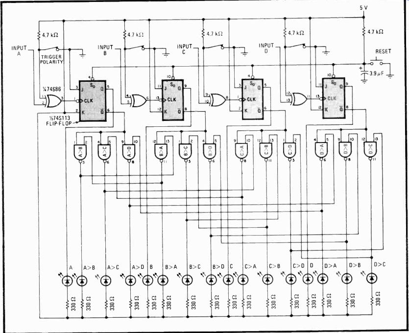
Signal sequence. Circuit indicates relative arrival times of four digital
signal inputs. Using Schottky TTL, unit resolves any two signals separated
by as little as 30 ns. Polarity switches at each input enable detection
of signal's rising or falling edges.
Four-chip meter measures capacitance to within 1%
by Peter Henry Seattle, Wash.
Measuring capacitance over the range of 1,000 picofarads to 1,000 microfarads, this four-chip meter has an overall accuracy of 1%. Costing less than $20, the unit has a digital readout and is built from parts that are readily available.

---------- Charge check. This digital capacitance meter measures
accurately over the range of 1,000 picofarads to 1,000 microfarads. The
circuit displays the number of pulses from astable multivibrator A2 in
the measurement count period during which 555 timer A, is active. The
measurements are repeatable to within a few counts on all but the lowest
scale, giving an overall accuracy to within 1%.
Engaging switch S1 momentarily fires timer A1, whose pulse width is determined by capacitor C1 and one of four timing resistors, R1 through R4. The timer enables an astable multivibrator, A2, and resets a three-digit decimal counter, which then counts the number of pulses from A2 until the timer runs out or a count of 999 (overflow) is reached. The number is then displayed.
A seven-decade range (see table) is achieved by switching in R1-R4, and R5-R6, which sets the frequency of A2 to approximately 1 or 1,000 hertz. For best performance, R1-R4 should be hand-picked to achieve the desired 1:10, 1:100 or 1:1,000 ratios if an accuracy to within 1% is required.
Calibration is achieved with a known capacitance of approximately 0.3 µF. Potentiometer R5 is adjusted for identical readings on the calibrating and 1-µF scale.
Then potentiometer R8 is adjusted for the same readings on both scales. This procedure is repeated as often as necessary for perfect agreement.
The circuit is very reliable and will yield repeatable measurements to within a few counts on all but the lowest scale. Differences in capacitance of 10 pF can be detected. Leaky capacitors may be difficult to measure because of their series resistance.
Time-slot assigner chip cuts multiplexer parts count
by Henry Wurzburg, Motorola Inc., Semiconductor Group, Phoenix, Ariz.
In some communications systems, particularly digital telephony equipment, it is hard to examine the data from a given source after it has been time-division-multiplexed with other data for serial transmission over a common data line. Capturing the data from its time slot and converting it into parallel form for examination usually requires many integrated circuits, since the slot must be programmable.
A special-purpose ic, the MC14417 time-slot assigner carries out this serial-to-parallel function with the aid of only a few inverters and one other ic. What's more, the cost of implementing the circuit is only a few dollars.
The timing of a simple three-slot TDM system is shown in (a). In digital telephone systems, a data frame may consist of anywhere from 24 to 40 time slots, each containing 8 bits of data transmitted at rates of up to 2.56 megabits per second.
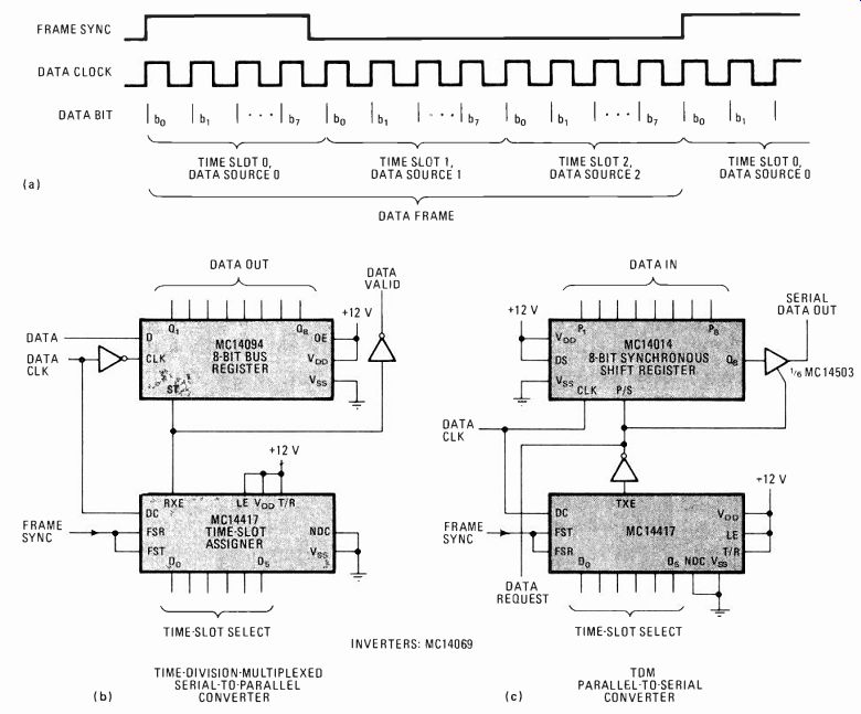
The right slot. Time-domain multiplexing (a) assigns to data from several
sources specific time slots in a serial data stream. Capturing data from
a specific slot is made easy with the MC14417 time-slot assigner (b),
which works with the MC14094 shift register to provide data from the
source dictated by the select inputs of the 14417. The versatile chip
can also provide parallel-to-serial multiplexing (c).
In the all-complementary-mos capture circuit of (b), the MC14094 shift register acts as a serial-to-parallel converter, while the 14417 computes when the data is to be captured and converted. Just which time slot it captures is determined by the binary data present at inputs D0-D5 of the 14417. The circuit also provides a valid-data output signal. As for speed, the circuit works for clock rates of up to 2.56 wiz with systems having up to 40 time slots.
Implementing a parallel-to-serial converter for multiplexing data onto the TDM data line is equally simple if the 14417 is used as shown in (c). Here, a three-state buffer prevents the serial data bus from being loaded during idle time-slot periods. The frequency limitations of this second circuit are the same as for the capture circuit.
Enhanced multiplier cuts parts count
by Guy Ciancaglini Fellows Corp., Springfield, Vt.
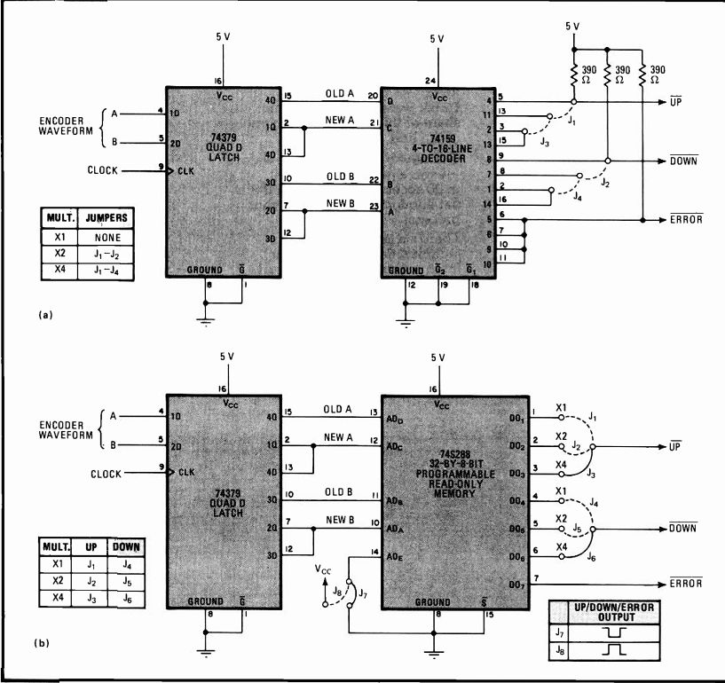
----------- Two versions. The encoder feedback multiplier (a) uses
transistor-transistor logic to save printed-circuit board space. The
TTL PROM version (b) costs a bit more, handles positive or negative true
logic, and needs even less board space. Both circuits are programmable.
The encoder-pulse-feedback multiplier circuit proposes by Frank Amthor [Electronics, Sept. 11, 1980, p. 139] and later simplified by Michael M. Butler [Electronics, Nov. 20, 1980, p. 128] may be implemented in a higher-speed TTL version that costs less and has fewer parts.
Butler's circuit reduced the original four-latch outputs to three lines so an eight-channel analog-multiplexer can be used. But the price paid was a space-consuming exclusive-OR package.
The TTL design implements the multiplier's common edge detector with a 74379 quad D-latch connected as shown in Fig. la. Furthermore, the 74159 4-to-16-line decoder enables it to use all four latch outputs, eliminating the exclusive-OR package.
Another plus for the TTL design is its versatility, which it owes to the fact that the collector outputs of the decoder are now open and may be hooked together in a wired-OR configuration. By including four jumpers or a dual-in-line-packaged switch, these outputs may be selected for one, two, or four times the original encoder feedback (see table). Since the decoder has a slower propagation delay than the latch frequency, the latch clock rate is limited to at most 25 megahertz.
Use of a PROM programmer can save even more space, but at a slightly higher cost. By replacing the decoder with a 32-by-8-bit TTL programmable read-only memory, the package is reduced in size and in pin count from 24 to 16 pins. The output pull-up resistors are also eliminated because of the PROM's three-state outputs. In this design variation, the X 1, X 2 and x 4 outputs are on individual lines. By making use of the fifth address input to the PROM, the output polarity may be set to positive or negative true logic using jumpers (Fig. lb).
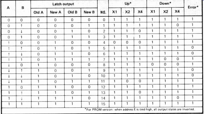
-------- TRUTH TARES FOR ENCODER MULTIPLIER
Pulse-width monitor flags poor timing
by T. G. Barnett and J. K. Stothers, Neonatal Research Group, London Hospital Medical College, London, England
Pulse intervals can be monitored to ensure they fall within a specified range by using two complementary mos 4098 dual monostable multivibrators. The original application of this circuit was to monitor biologically produced pulse trains. However, the principle can be applied to any case where it is necessary to know if the limits of a pulse interval have been exceeded.
The 4098 is two independent one-shots in a single package and each one-shot has leading- and trailing-edge triggering, re-triggerable and non-re-triggerable modes as well as a reset and complementary outputs.
These facilities have been incorporated within a monitor that senses whether a pulse train has intervals longer or shorter than those of a chosen range.
The period of each one-shot may be obtained from its data sheet or approximated by:
T(time) = 0.5 X RC for values of C>0.01 microfarad.
The value of the capacitor should be as small as possible and the resistor should not be more than 10 megohms. All unused inputs must be connected to either the drain- or source-supply voltage in accordance with the data-sheet instructions.
As the circuit in the figure shows, monostable A1, operated in the re-triggerable mode, is triggered on the leading edge of an input pulse. The i output is normally low unless the input-pulse interval is greater than the duration of the monostable's pulse-width value, set by resistor R1 and capacitor C1. If the pulse interval exceeds this value, then Q will go high, resulting in the output of the 4071 OR gate going high. Thus the maximum interval time is set by this monostable.
The leading edge of the input pulse also triggers monostables A2 and A3, both of which are operated in the retriggerable mode. Output Q of A2 acts as a delay and is fed into the trailing-edge-trigger input of A4, whose Q output drives the reset pin of A3. The delay that is caused by A2 is a few microseconds and prevents A3 from being triggered on receipt of the leading edge of the input pulse, as its reset pin is low until A4 is triggered. A4 is operated in the nonretriggerable mode and sets the minimum-pulse-interval time.
The Q output of A3 will go high only if its reset pin is set high by A4, whose Q output will go high only a short time after A3 has received a trigger pulse. However, if a further input pulse is received within the time the Q output of monostable A4 is high, then monostable A3 will be triggered, its Q output will go high, and the 4071 OR gate will go high. The actual pulse width of A3, set by R3 and C3, can be chosen to suit any application.
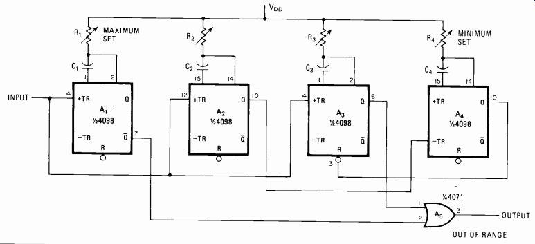
---------- 1. Watching it. Out-of-bounds time intervals between a
train of pulses are detected at OR gate A5 because one-shot A, stays
triggered unless the time between pulses is too great. Meanwhile one-shot
A3 triggers if it receives successive pulses too soon. It also drives
the OR gate
Improving the LM395 for low-level switching
by Yehuda Gabay Israel Atomic Energy Commission, Beersheba, Israel
The most significant drawback of a power transistor like National Semiconductor's LM395 is its relatively high quiescent current (10 milliamperes or so), which makes it impossible to use as a reliable switching device for small loads or loads that require dynamic currents ranging from zero to some high value. Adding a transistor-diode network and an optocoupler to the circuit, however, adapts the LM395 as a low-level (down to 0-mA) switch without sacrificing the current-handling capabilities of the power transistor and provides input-to-output isolation as well.
This circuit is configured as a normally-off switch whose quiescent load voltage is a maximum of 0,6 volt.
Placing a logic 1 at the input of optocoupler U1 causes transistor Q1 to turn off. Thus the power transistor, Q2, conducts and the desired current flows through the load, RL.
If the input to the optocoupler goes to a logic 0, Q2 cuts off and no current flows through the load. In this state, Q1 conducts and the quiescent current of Q2 that must flow is shunted through diode DI and through Q1 to ground. It should be noted that D2 bypasses transients to ground that are caused by an inductive load.
In the case where the user desires to implement a normally closed switch, it is only necessary to remove the circuitry centered around Q. Then, U1's output transistor will serve. to bypass Q2's quiescent current to ground when necessary.
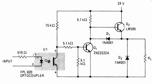
------- Bypass. A floating switch in the form of
an optocoupler adapts power transistor Q2 for handling small load currents,
directing transistor Q1 to bypass Q2's high quiescent current (10 mA)
when a logic 0 is applied to the circuit input If a normally on switch
is desired, Q1 and its associated circuitry need only be removed. U1's
output transistor then will take Q2's quiescent current to ground.
Contact tester quantifies open-, short-circuit tendencies
by Steven Nirenburg and Wunnava V. Subbarao Florida International University, Miami, Fla.
Many present-day electronic systems, being modular in nature, rely heavily on connector blocks to hook the various functional units together. As such, it is becoming increasingly important to detect any momentary open circuit or short-circuit tendencies of the system at the connector-especially in high-vibration environments both in production-line testing and during actual operation. This tester detects both, while indicating if either condition persists beyond a given time preset by the user.
Consider the detection of an open-circuit tendency of contact S1, as shown in the figure. For the purposes of discussion, the open-circuit condition is arbitrarily chosen to be one in which the resistance across S1 is greater than 10 ohms for a period equal to or greater than 100 microseconds.
On system reset, the 74192 counters and 7476 flip flops are brought to logic 0. If S1 is closed, voltage V1 will be near zero and the outputs of comparators G1 and G2 will be high. Light-emitting diode Do then glows, indicating the contact is closed.
If S1 is momentarily opened or shows any contact deterioration, V1 rises slightly above ground potential, forcing G1 low and gating the output of the 1-megahertz clock through to the counters. Thus should the contact deterioration last for 100 ;Ls, 100 clock pulses will be counted and the resulting carry pulse generated from the second 74192 will set flip-flop F1. And if the ohmic resistance across S1 goes above 10 S2, V1 will rise above 50 millivolts, forcing G2 low and flip-flop F2 high.
Thus D1 will glow if F1 is set and F2 is clear. D2 will glow if F1 is clear and F2 is set. D3 will light if both F1 and F2 are set, so that the predetermined open-circuit time and resistance of S1 may be readily recorded.
Short circuits are readily detected by connecting points A and B across the normally opened contact under test. When the contact is open, V1 is near zero and the system remains in the reset position, lighting up D0. If shorted momentarily, S1 will cause either D1, D2 or D3 to light. For the values shown in the figure, D1 will glow if the short circuit exceeds 100 its or more; D2 indicates if S1's resistance is less than 1 mi2; D3 illuminates if both of the aforementioned conditions exist.
By changing the clock frequency or the counting limit, any time interval can be preset. Similarly, the impedance at which the circuit responds may be selected by adjusting the threshold voltage at G2.

------ Connection. Tester for block connectors, pc boards, and cable
assemblies indicates if duration of open or short circuit in circuit
pin or lead exceeds preset time and checks relative magnitude of resistance
across switch or broken wire. Four LEDs indicate state of affairs.
PLL performs accurate phase measurements
by N. H. Sabah, Engineering and Architecture Faculty, American University of Beirut, Lebanon
The excellent tracking ability inherent in a phase-locked loop is utilized in this meter to measure phase differences accurate to 0.1°. Although intended for use in the dc-to-l-kilohertz audio-frequency range, the upper limit of the unit can be extended by suitable selection of a high-frequency PLL and appropriate circuitry to reduce phase jitter.
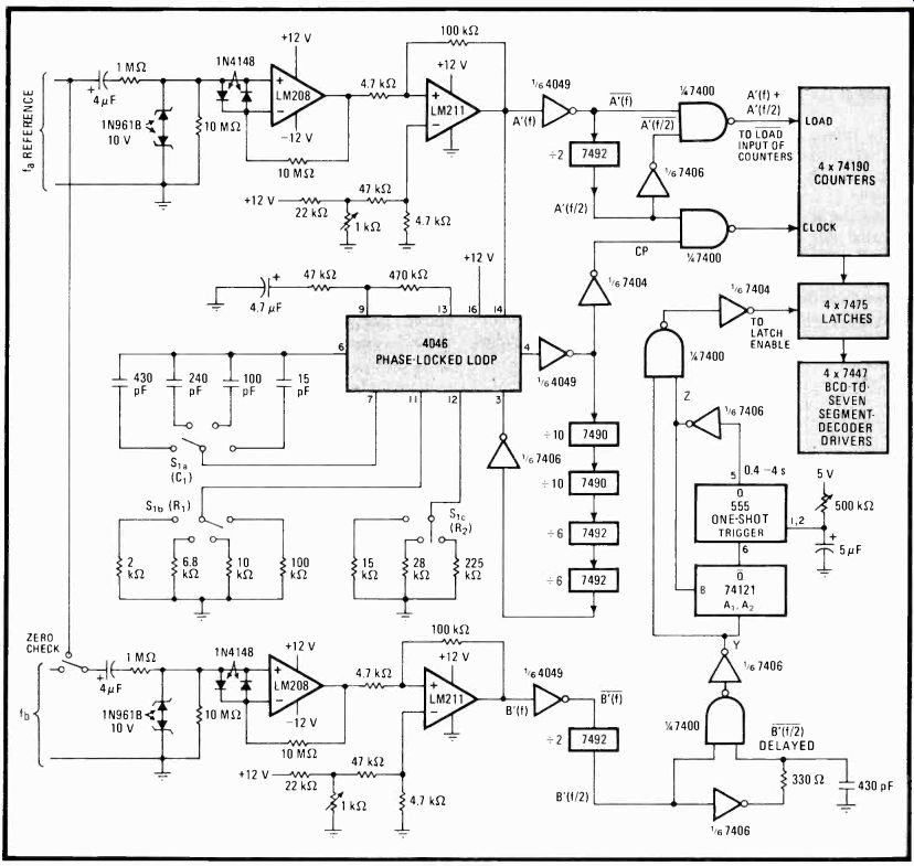
----------- Angular accuracy. Meter utilizes tracking ability of
PLL to perform phase measurements accurate to 0.1°. 4046 delivers clock
signal equal to 3,600 f, to conventional display (not shown), where count
time is determined by fb. Thus phase angle of fb with respect to f. is
displayed.
The reference and the signal to be measured, fa and fb respectively, are applied to the LM208 operational amplifiers, which form the isolating stages. The LM211 comparators that follow provide a rise time of less than 100 nanoseconds and a phase-shift equivalent time between points A'(f) and B'(f) of less than 20 ns. A zero-phase check switch is provided so that the reference may be applied to both channels simultaneously. This allows the user to minimize the aforementioned offset time with channel B's 1-kilohm potentiometer, which is located at the input of its corresponding LM211 comparator.
The reference waveform is then applied to the 4046 PLL, which has a 3,600:1 frequency divider in its feed back loop. The output of the 4046 is thus 3,600 fa and is virtually in phase with the incoming signal. In order to reduce the phase jitter to a minimal value, the PLL is operated over four ranges selected by means of switches S 1a to S1c (see table).
The output of the 4046 serves as the clock for driving a four-digit display circuit, which can be made up conventionally with cascaded sections of 74190 synchronous up/down counters, a set of 7475 4-bit bistable latches, 7447 BCD-to-seven-segment decoder/drivers and suitable displays. (The one-chip ICM7217 provides the counter, latch, and decoding functions and could conceivably be used to reduce the chip count, but requires multiple supply voltages.) The count is initiated on the rising edge of fa and is terminated by the leading edge of a pulse from channel B. Pulses are counted on alternate cycles of the incoming wave, to minimize control circuitry. Because the circuit is designed for steady-state phase measurements, there is no loss in accuracy. The (lagging) phase angle of fb with respect to fa is then displayed. The 74190 counter circuitry may be simply modified to preset the counters to 360 in the countdown mode, instead of counting up from 0, so that the phase of fa with respect to fb may be shown. Flicker is eliminated by appropriate selection of the 555 one-shot's timing components.

--------- PHASE METER'S RANGING COMPONENTS
Interfacing TTL with fast bipolar drivers
by J. A. R. Ball, P. J. Grehan, and P. Welton, Darling Downs Institute, School of Engineering, Queensland, Australia
Surprisingly, there are as yet no suitable integrated circuits for translating the 0-to-5-volt output swing of TTL into arbitrary bipolar levels. But even the discrete interfacing circuits that have appeared over the years will fall short in performance, especially if the requirement calls for a high-speed switch to drive the relatively high capacitance of a power device or load. The solution lies in modifying the typical textbook interface with a circuit that acts to decrease the input-circuit storage time of the output transistors but does not appreciably affect any other interface parameter or specification.
A slightly modified ± 10-v TTL interface is shown in (a), which will be suitable for relatively high-speed switching at low to medium current (below 100 milliamperes). In this circuit, Q1 turns on and remains in the active region when the TTL output exceeds 1.5 v. Providing the current drawn out of the base is sufficient, Q3 will saturate and the voltage applied to the load will be almost 10 v. When the TTL output falls sufficiently, Q1 and Q3 turn off, and charge stored in the base of Q3 escapes via resistor R3. Transistors Q2 and Q4 comprising the other half of the circuit act in a complementary fashion, conducting when the TTL output falls below 1.5 v and applying-10 v to the load.
One disadvantage of this circuit is that it is possible for ,Q3 and Q4 to be conducting at the same instant during a change of state to cause a supply current spike whose magnitude may exceed the nominal load current by more than three times. Also, most of the power lost in the output transistor will be dissipated during a change of state when both are in the active region. Thus, the average dissipation will be proportional to the switching frequency. These problems may be minimized by increasing the zener voltage, Vz, so as to increase the dead zone between the input threshold levels of the circuit. Switching speed may be increased by optimizing the value of the speed-up capacitors C1 and C2, operating Q3 and Q4 at very large base currents, and reducing R3 and R4 to minimize storage time.
This basic circuit can also be used to control far larger currents than 100 MA, providing appropriate output transistors are used. However, the storage time of these devices then becomes a major problem, and so speed is sacrificed. The circuit in (b) shows how to reduce the delay time by adding two transistors for supplying reverse base current to whichever output transistor is in the act of turning off.
Here, when the TTL output goes high, Q1 conducts and Q3 saturates as before, while Q2 turns off and Q4 begins to come out of saturation. In addition, the emitter current of Q1 turns on Q6, which provides a path for the escape of charge stored in the base of Q4. This effectively 'shortens Q4's turn-off delay.
When the TTL output goes low, then Q1 and Q6 turn off, Q2 and Q5 conduct, Q4 saturates because of the base current supplied by Q2, and Q3 is rapidly turned off because of the action of Q5. Discharge transistors Q5 and Q6 should be selected for high-speed saturated switching, so that they will not delay the turn-off of their associated output transistors.
Adding Q5 and Q6 will reduce the storage delay of the output transistors by a factor of from 2 to 4. The circuit in (b) provides a rise and fall time of about 80 nanoseconds for a load of 11 ohms (2-ampere load). The active pull-up output ensures the interface's low output impedance in either the logic 0 or logic 1 state. A further advantage is that the output voltage is specified within narrow limits in both states, unlike the case with totem pole-type circuits.
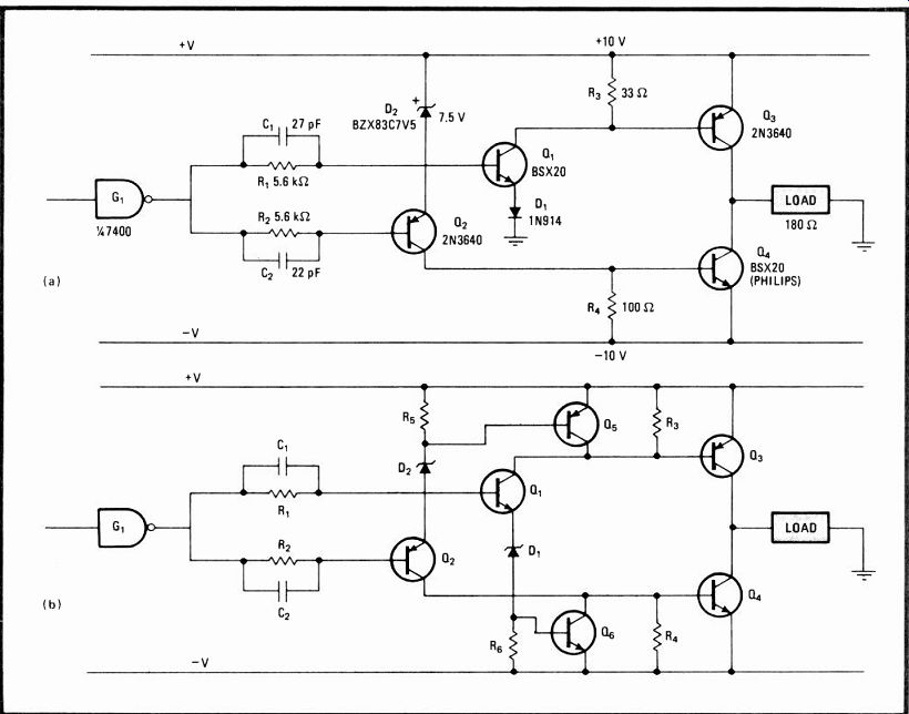
----------- Conversion. Interface (a) for translating
the 0-to-5-V TTL swing into arbitrary bipolar levels at moderate switching
speeds works well at low load currents. For increased loads, circuit
(b) offsets the large storage delay of the output transistors and reduces
crossover switching.
Adapter equips HP analyzer for general ROM tracing
by Israel Gal Liad Electronics, Moshav Yaad, Israel
A two-socket adapter turns the popular Hewlett-Packard family of HP1611 A logic analyzers-which can normally be configured for debugging one specific micro computer-into a general-purpose read-only-memory tracer. Thus, as this example shows, it can be used with the Z-80 Personality Module as a developmental tool for Intel machines, without the need for Intel's ICE series of in-circuit emulators.
Tracing is simply achieved by placing the microprocessor's address and data lines directly in parallel with those of the external program memory and disabling all other input lines to the Z-80. Placing a low-insertion-force socket, such as those produced by Textool Inc., at the Z-80 end enables fast connection to the conversion circuit. At the memory end, use of a hardwired 24-pin spring clip adds increased flexibility for in-field testing.
Also recommended is a scope probe for latching onto the appropriate circuit point of the desired clock signal. The clock and its inverse signal are available, so that the user can synchronize the timing to each particular processor.
In operation, the logic analyzer will be synchronized as usual to accept address, data, and external information in every possible combination. Thus, most of the additional options of the analyzer, such as pre-triggering, post-triggering, trace and count triggering, and trigger enable and disable can be utilized. The single-step and trace-then-halt options of the Intel 8031-8051 machines cannot be used here, although they will be functional on every other processor that has a wait line.
Using the HPI611A this way has several drawbacks, among them the fact that there is no disassembly information is displayed in hexadecimal or octal format.
And the information shifted onto available on-chip RAM or registers is not itself displayed, only the representation of the transfer as an operating code. Also, as a result of the clocking arrangement, there can be situations where the directive will be displayed twice (although the address is always correct). However, where low cost, convenience, and efficiency are important, this circuit is satisfactory.
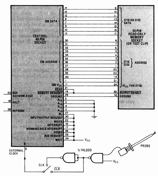
-- --- Translator. Parallel connection of data and address lines of external
memory with HP161 1A logic analyzer through appropriate inter face eases
debugging of any microprocessor-based system by a dedicated analyzer.
Scheme has drawbacks-lack of disassembler, the fact that shifted information
cannot be actually displayed, and occasional multiple display of op code
directives-but is cheap, convenient, and efficient.
LED indicates timing error in emitter-coupled-logic one-shot
by M. U. Khan Systropics, Naroda, Ahmedabad, India
Rather than scrutinize waveforms on an oscilloscope, it is possible to employ a simple circuit to monitor the output of a one-shot to determine if it is being triggered at the right time or if the output pulse width is correct.
If the clock pulse arrives while the normally low output Q1 or set line S1 of the one-shot is at a logic 1 level, the Q2 output of the indicator flip-flop goes to a logic 0 level, turning on the light-emitting diode. Q1 of the one-shot remains at the logic 1 level only in its quasi-stable state, whereas SI goes to the logic 1 level only in its recovery state. Thus whenever the one-shot is triggered too early-in other words, before recovering the LED turns on. When the mis-triggering is corrected, by reducing either the clock rate or the width of the one-shot, it automatically turns off.
Besides the LED, the indicator circuit consists of an MC 10103 oR gate and an MC 10231 D-type flip-flop, both emitter-coupled-logic devices. The circuit works satisfactorily up to 75 megahertz. For higher speeds-up to 100 MHz-propagation-delay compensation through an additional oR gate (dotted line) is needed. In the latter case, both the oR gates should be replaced by an MC 1660 dual four-input oR-NOR gate.
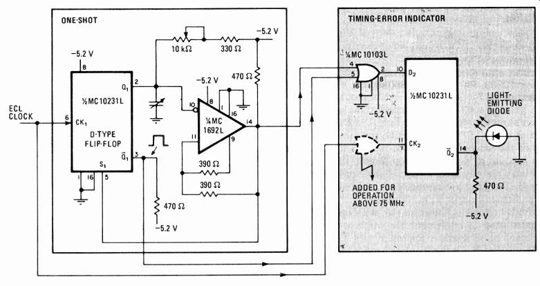
---------- Hot shot. Spotting timing errors in a fast one-shot multivibrator
is simplified with the addition of an error indicator circuit such as
the one shown in the shaded area. If the clock rate is too high or the
output pulse width is too small, the LED will Indicate it.
Wired-OR ECL one-shot has near-zero propagation time
by Jozef Kalisz Warsaw, Poland
Because of their output configurations and current-handling capabilities, emitter-coupled-logic and TTL circuits can easily yield the wired-oR function simply by having the outputs of two gates tied together. This trait may be employed to build a pulse-stretching circuit in either logic family that is equivalent to a monostable multivibrator having virtually zero propagation time.
Such a circuit, shown in (a) for ECL, relies on the positive-feedback loop created by gates G1 and G2. In the steady state, the input voltage of G2 is maintained at the V1N level of about -1 volt by resistors R1 and R2.
The positive input trigger pulse, derived from a typical ECL gate, brings the driving-point potential to - 1.8 v, permitting capacitor C to charge.
As long as the input voltage to G2 remains below about - 1.3 v, the gate's output voltage will be high, thus stretching the input pulse. If the propagation time of the gates is not taken into account, the output pulse width is approximately equal to T = 0.98 CRII1R2. With the gates in the 10000 logic family, the minimum pulse width of the driving pulse can be made 4 nanoseconds, which is equal to the propagation time in the loop. The circuit may directly drive a coaxial cable or a microstrip line, provided they are correctly terminated. In such a case, pull-down resistor R4 is not required.
A similar circuit is shown in (b), with open-collector TTL gates used to implement the wired-AND function.
The output pulse width is approximately T = 0.28 X CRIIIRIL, where RH, is the input resistance of G2 when its input voltage remains below the 1.4-v threshold. Typically, RIL = 4 kilohms. The shortest input pulse required is about 20 ns, and this value again is equal to the circuit's propagation time.

--------- Infinitesimal. Wired-OR connection of emitter-coupled-logic
gates (a) permits the building of a pulse-stretching circuit that is
equivalent to a one-shot having virtually zero propagation time. In this
case, it is 4 nanoseconds, equal to that of the minimum pulse needed
to excite the circuit. Similar results are derived from wired-AND gates
of TTL (b), although the propagation time is a bit longer-20 ns.
Twin optocouplers raise serial transmission speed
by Luis E. Murguis Autotrol SA, Buenos Aires, Argentina
In a balanced 20-milliampere current loop for long distance serial data transmission, optical couplers are a convenient way of connecting both receiver and transmitter to the transmission line, and provide isolation as well. However, an active pull-up scheme employing an additional optical coupler at the receiver can improve transmission speed by an order of magnitude.
In the setup shown in (a), the fall time of the output voltage depends on the saturation current, I of the coupler's input. However, the rise time of the output voltage, which determines the maximum transmission frequency, corresponds to the turn-off time of the coupler's output and is a function of load resistor R.L.
Lowering the value of R1 raises the transmission rate, but only up to a limit set by the amount of current the optical coupler can handle.
Instead of trading off transmission speed and coupler loading, a second optical coupler produces a faster rise time and improves the transmission frequency almost 10 times over systems configured in the conventional way.
The two optical couplers are connected as shown in (b) to produce an active pull-up and pull-down circuit at the output and thus speed up the output-voltage rise time.
Both the rise and fall times are now a function of I1, as the couplers alternate between their on and off states.
Resistors R1 and R2 are optional and provide a fixed bias in case a circuit failure causes Ii to fall to zero. Another advantage of this circuit is that it improves fanout since a load resistor is no longer needed. 1
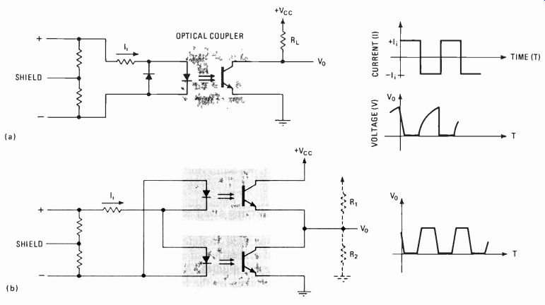
---------- Active output. A conventional, single-coupler design for
a 20-milliampere current loop (a) limits the transmission rate because
the signal rise time is a function of resistor Using two couplers in
an active pull-up output (b) forces faster rise times and hence higher
transmission rates.
Digital phase meter updates measurement each cycle
by R. E. S. Abdel-Aal, Department of Electronic Science, University of Strathclyde, Glasgow, Scotland
Because this meter measures the phase delay between two low-frequency square waves once every cycle, it is useful in applications where instantaneous readings of this delay are continuously required. The circuit resolution is within 1% for signal frequencies of up to 250 kilohertz.

---------- 74LS123 DUAL MONOSTABLE Instantaneous. Circuit continuously
compares phases of two incoming square waves, providing a 15-bit and
plus-sig resolution of (f,./250)%. With a 25-MHz clock, the practical
upper frequency limits that can be handled for incoming signals is 250
kHz, with lowest-frequency boundaries being about 400 Hz. Lower limits
can be reduced further by decreasing the clock frequency.
Generally, the meter counts the number of pulses of a 25-megahertz clock for a time equal to the phase delay between the two incoming waveforms. Then it strobes the measured value into output latches once a cycle. The result is a continuously updated value expressed as a 15-bit binary number plus a sign bit.
To achieve this, the cycle is viewed as one that varies from plus to minus 180°. By using only one half of the cycle for measurement, the circuit is free during the other half to store the results in the output latches and to clear the phase counters for the next measurement.
The circuit automatically determines which of the signals is to be the reference, with the phase delay measured from the rising edge of the leading signal to the rising edge of the lagging waveform. The falling edge of the reference serves as the latching signal and to set up the counters for the next cycle.
In operation, the two incoming signals, A and B, are applied to two gates of A1. Here, the complemented signals A and B are obtained with negligible differential delay. The other two gates in the chip generate gating signals corresponding to AB and AB. Flip-flop A2 determines which input signal is the reference.
If A leads B, then the Q output of A2 goes low and gating signal AB, together with input signal A, drives the 74LS157 selector chip, A3. Otherwise, gating signal AB together with input signal B will be selected.
The selected phase-gating signal is used to enable a chain of synchronous counters, A4-A7, which are driven from a crystal-controlled 25-MHz clock built around three inverters in A8. When the phase-gating signal drops, A.-A, stop counting, holding their final result, which indicates the phase delay, at their parallel outputs.
Following this, a short pulse from one-shot AM latches the results of the count in Ali, and A . Then the pulse-counter chain is cleared by a second pulse from A9B. To ensure a proper count and store cycle, the sum of the widths of the two short pulses should be less than half the period of the highest-frequency input signal. Also, the short pulse used to clear the counters should be greater than the clock period.
The upper limit on the frequency of the input signals is set by the resolution of the phase measurement that can be tolerated. With this circuit, the resolution is given by (f/250)%, where f is the frequency in kilohertz.
The lower limit of the signal frequency is set by the overflow of the phase counters before the end of half a cycle of the input signal (that is, the maximum phase delay measured). With a 25-MHZ clock and a 15-bit binary number representing the magnitude of the phase (excluding the sign bit), the minimum input frequency will be 25(10^6)/(2(2^15-1)) = 381 hertz. At low input frequencies, however, a lower-frequency clock can be used while maintaining good resolution, and thus the frequency limit can be brought down even further.
[source: ISBN 0-07-606808-0 Copyright 1982 by McGraw-Hill, Inc. ]