
By J. A. "Sam" Wilson. CET
Many industrial electronic devices have digital circuits. Therefore, the next few articles will present practical digital information.
Linear Versus Digital
Electronic circuits can be divided into the two broad categories of linear or digital.
Linear operation
Linear circuits operate with many different levels of input amplitude and output amplitude. The output amplitude varies in step with changes of the input amplitude. (For example, even small changes of input level cause changes of the output amplitude.) Of course, the output signal can be either in-phase or out-of-phase with the input; and the gain either can be more or less than one. In most cases, each linear stage has a voltage gain or a power gain.
Input and output signals can have any desired waveshape or amplitude. Linear operation often is called analog.
Digital operation
Digital circuits have fixed amplitude levels of input and input signal voltages. In fact, they can't operate at any other levels.
Most popular is the binary digital-logic circuit. Each device has an output level that's either HIGH or LOW (with nothing between). HIGH also is called ON or 1, and LOW often is referred to as OFF or 0 (zero). We will use HIGH and LOW for the text, and 1 and 0 for tables and mathematics.

Figure 1 The Hewlett-Packard model 545A Logic Probe has a switch for
selecting TTL or CMOS families of digital signals, plus a latch circuit
that can be switched in to hold the indication.
An LED (mounted near the tip) lights for logic 1 (HIGH) states.
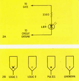
Figure 2 Most logic probes light to indicate a HIGH (logic 1). The most
simple probe is shown at (A). It does load the circuit somewhat. Next
month we'll describe a better one. (B) These are the probe symbols used
in the next few articles. Logic 1 (HIGH) produces a bright light; the
LED or lamp is dark for a logic 0 (LOW); pulses are shown symbolically
by the half-dark, half-light circle (however, with real probes, pulses
produce either a dim light, or a regular flashing on and off, depending
on the type of probe); and during the troubleshooting questions, un known
states are indicated by a question mark.

Figure 3 Troubleshooting Question #1: Which diagram shows the correct
logic probe indications?
Remember that the numbers 1 and 0 do not refer to voltage, or to a voltage value, but merely to different levels of signal.
Digital stages usually have square or pulse waveforms, and the input and output levels are equal (in other words, the gain is 1). The repetition rate or duty cycle of the waveform might change during operation, but the amplitude levels remain constant.
Either the top or bottom of each digital waveform is at zero voltage; therefore, the signals can be thought of as pulses of DC voltage.
By comparison, capacitor-coupled and transformer-coupled analog pulses have the zero-voltage line near the center, with the exact location determined by the duty cycle. A square wave has half of its amplitude above the line (positive) and the other half below the zero line (negative).
Digital Troubleshooting
In some digital equipment, manual switches or sensors determine the various HIGHs and LOWs.
Therefore, the desired states can be selected, and then not changed during the testing time. The HIGH and LOW states can be measured by a DC voltmeter or the DC function of a scope.
However, meters and scopes are slow in operation. Also, extreme accuracy of the DC voltages is not required (a HIGH can be any voltage between 80% and 100% of the supply, and a LOW might have any voltage from 0% to 20% of the supply voltage). Another disadvantage of meters is that continuous pulses read as an intermediate DC voltage. A logic probe is the answer to most of these problems.
Logic probes
A logic probe can indicate a HIGH, a LOW, or a pulsating digital signal. The indicator (usually a LED, or several colors of LED) is located near the probe tip where you can see the light without looking away from the pin of the IC you are testing.
----------
BINARY COMPONENTS
Component relay lamp vacuum tube transistor MOSFET diode switch
Logic 0
Logic 1 not energized--energized off on cut off saturated cut off saturated cut off saturated reverse biased forward biased off on

Table 1 Many commonplace components can be used in binary systems.
----------
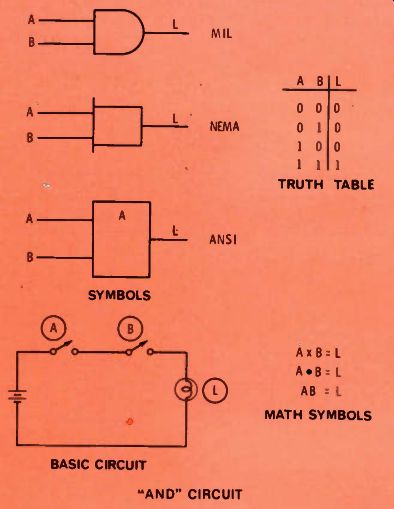
Figure 4 An AND gate produces a HIGH output only when both inputs are
HIGH. The math formula is read as: A AND B equal L.
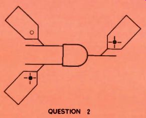
Figure 5 Troubleshooting Question #2: Is the AND gate working properly?
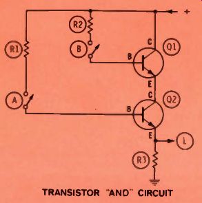
Figure 6 Two transistors can make up an AND circuit. Both switches must
be on (HIGH) so both transistors can conduct the supply voltage (HIGH)
to the output load, R3.
One commercial probe is shown in Figure 1. You can build your own simple probe (Figure 2A). Of course, it only identifies HIGHs, LOWs and pulses, while some of the manufactured models can be adjusted for the family of devices you want, and they have sophisticated circuits (such as pulse stretchers) that permit more accurate additional tests.
Digital signals that have a constant stream of pulses should be viewed with a scope; a logic probe will indicate the pulses are there, but can't measure the duty cycle, the repetition rate, any distortion of the waveform, or the presence of noise.
Tests with a probe can be made very rapidly; therefore, such probe tests usually are done first. If they can't find the source of the defect, a scope should be used next.
Troubleshooting questions
Troubleshooting questions with schematics will be inserted at appropriate points in this series.
Logic probes will be shown making the measurements. We assume a ground connection (plus the supply voltage, where one is required for the probe); therefore, only one connection to the tip of the probe will be indicated.
Figure 2B lists the probe symbols we are using to indicate the HIGHs, LOWs, and pulses.
Supply voltage--HIGH or LOW?
In many logic circuits, the supply voltage is marked Vcc for collector voltage, if bipolar transistors are used. Or, it's marked VDD, if it is the drain voltage of MOSFETs. As a general rule, the positive power supply voltage is considered to be logic 1 (HIGH), and the common (ground) connection is logic 0 (LOW). (Answers for the troubleshooting questions are listed at the end of this article.) Binary Operation Binary digital circuits are used extensively in logic systems, especially with industrial devices. Many components can operate only at two levels. Others can be forced to operate at two levels only.
The components of Table 1 are used in the basic logic building block circuits called GATES.
There are seven basic GATES, and you should memorize their characteristics if you want to be come proficient in servicing logic systems. These GATES are: AND; INCLUSIVE OR; NOT; NAND; NOR; EXCLUSIVE OR; and LOGIC COMPARATOR. The first three are covered in this article.
Four characteristics of these basic gates will be described in detail: the schematic symbols, the math formula symbol, the truth table, and a typical circuit showing the operation.

Figure 9 INCLUSIVE OR gates have a HIGH output when either or both inputs
are HIGH. The math formula means: A OR B equals L.

Figure 10 (A) Here an INCLUSIVE OR gate is wired with a relay and switches,
using electronic symbols. (B) The same circuit is drawn this way when
industrial symbols are used.
Unfortunately, three different types of circuit symbols are used in industrial electronics. Therefore, all three will be shown. You most likely will be working with MIL symbols, but you should learn all three kinds.
AND Gate
The AND gate of Figure 4 has inputs A and B, plus the output L (for load). This is a binary system having only two possible levels of input and output signals. Both inputs must be HIGH to obtain a High output.
Truth tables provide maximum information in a minimum space.
All combinations of input HIGHs and LOWs are listed at the left, and at the right is shown the output state that results from those inputs.
Of the four possible combinations, notice that only one gives an output.
AND circuits can be constructed from many different kinds of components, including transistors or tubes. But, the basic circuit operation can be demonstrated with only a battery, two switches and a light bulb, as shown.
Don't read the math formulas as "A times B equals L." With logic AND circuits, the multiplication sign represents AND. Therefore, all three math examples read "A AND B equal L." An AND gate made with two transistors can be wired as shown in Figure 6. Because they are NPN transistors, a positive voltage (HIGH) is required at both bases to saturate the collector current (HIGH). When both transistors are saturated, the B+ goes through them to the output load, R3. A zero voltage (LOW) at either or both bases stops the current flow in either or both transistors, giving a zero-voltage output (LOW). Use your analog skills to trace the circuit operation, and prove to yourself that it conforms to the specs for AND gates.
AND industrial symbols
Figure 7 contrasts an AND gate drawn with conventional electronic symbols (A) to the same circuit (B) with industrial symbols. Input A and input B both must be HIGH (logic 1) to produce a HIGH at the lamp.
Ladder diagrams (similar to Figure 7B) are easier to read when the circuit is complex, and it can be drawn smaller than the usual symbols can. All of the contacts of the relay are marked with the same letter as the relay coil symbol.

Figure 11 Paralleled transistors can function as an INCLUSIVE OR circuit.
Conduction of either or both transistors brings the supply voltage to
the Output R3.
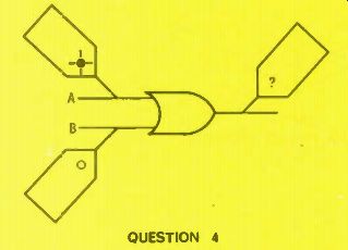
Figure 12 Troubleshooting Question #4: Assuming that the OR logic gate
is working correctly, what indication should the probe show?
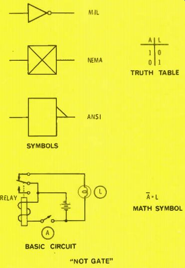
Figure 13 These are the important characteristics of NOT gates (or inverters).
The output state always is opposite to the input state.

Figure 14 (at left)
When industrial symbols are used, the schematic of Figure 13 appears this way.
Figure 15 (at right)
Troubleshooting Question #5: What should the logic probe indicate?
INCLUSIVE OR GATE
The four characteristics of IN CLUSIVE OR gates are given in Figure 9. A HIGH at either or both A and B inputs produces a HIGH at the output of an INCLUSIVE OR gate.
Our normal language does not make clear the differences between an "inclusive or" and an "exclusive or." For example, if someone says, "John or Mary can go to the store," and the intent is to say that either or both can go, this is the inclusive form. But, if the person intended to say that one or the other can go (but not both), the exclusive form was needed. Both forms are used in logic circuitry.
When either or both switches in the basic circuit are closed (HIGH), the bulb lights (HIGH). The math formula A -1- B = L means A or B equals L (it never should be read as A plus B). Figure 10 shows both the conventional schematic of an INCLUSIVE OR gate with a relay, and the same circuit using industrial symbols.
Transistors can operate as an INCLUSIVE OR gate (Figure 11). When a switch brings forward bias to either or both bases, the saturation current applies nearly full supply voltage to the output, R3.
INVERTER (or NOT) Gate
Figure 13 gives the characteristics of NOT gates, also known as INVERTERs, which have only one input and one output. The output logic level always is opposite to the input level.
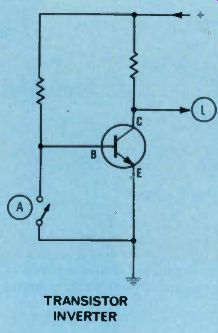
Figure 16 A common-emitter transistor can function as a NOT gate.

Figure 17 (at right) (A) Dual-In-Line Package (DIP) ICs have rows of
pins down each side. Pin-out numbering from the top is counter clockwise
from the marked end. (B) Hex NOT gates contain six separate gates, which
can be operated (below saturation) as amplifiers.
In the relay basic circuit, closing switch A (HIGH) energizes the relay coil, and it opens the NC contact to open the lamp circuit (LOW). The ladder diagram in Figure 14 is the same, but with industrial symbols.
An overbar, as shown in the math symbol, always indicates that the letter (or letters) below it are negated. For example, the expression A is read "NOT A." A double overbar indicates a double inversion, to be read "NOT, NOT A," and is identical to A. A NOT gate can be constructed by using the inversion of a transistor (Figure 16). Closing switch A removes the forward bias (LOW), and cuts off the collector current.
Therefore, the collector voltage at L rises to the supply voltage (HIGH). The circuit of Figure 16 also illustrates an important point about other uses for inverters. Although they are intended for operation either saturated or cut off, most can be used (below saturation) as amplifiers. Hobbyists enjoy opera ting them in trick circuits.
Hex inverters, in DIP form, contain six separate inverter amplifiers (see Figure 17). Correct pin out numbering also is shown in the same illustrations. Most trouble shooting of ICs is done above the board; therefore, you should locate the identified end of the IC, and start counting at 1 and upward in a counter-clockwise rotation. Usually, pin 7 is grounded, and the B+ enters at pin 14 of 14-pin ICs, although many schematics omit the ground and B+ connections.
Lab Projects
As this digital-logic series progresses, we will show you several experiments that can be performed easily at home. Plug-in circuit boards (such as the two shown in Figure 18) are very convenient for performing these experiments.
The following companies manufacture experiment boards:
AP Products, Incorporated Box 110, 72 Corwin Drive, Painsesville, Ohio, 44077
Continental Specialties 44 Kendall Street, Box 1942, New Haven, Connecticut, 06509
You could write for a catalog describing the boards and other items useful in logic work. Many local electronic distributors stock them, and several kit companies incorporate them into complete systems.
The first experiment will be described at the beginning of the February article.
Answers To Troubleshooting Questions
#1-The probe indications of Figure 3B are correct. Usually the negative terminal of a power supply is common, or ground (LO W); therefore, the positive supply line is HIGH.
#2-In Figure 5, the AND gate is not working properly. The input probes show one HIGH (logic 1) and one LOW (logic 0), so the AND gate should have a LOW (logic 0) output.
#3-The probe LED should be lit, indicating a HIGH (logic 1) output. The circuit of Figure 8 is a relay AND gate; therefore, both input switches turned on (HIGHs) should produce closed relay contacts, and a lighted lamp (HIGH output).
#4--The probe should indicate a logic 1 (HIGH), because the gate of Figure 12 is an OR. The inputs are 1 and 0 (HIGH and LOW), and either or both inputs HIGH should produce a HIGH output.
#5--When switch A is open (LOW), the probe should indicate a logic 1 (HIGH) at the lamp output of the relay NOT gate (inverter). With NOT gates, the output state always is opposite to that of the input. Therefore a LOW input produces a HIGH output. 0
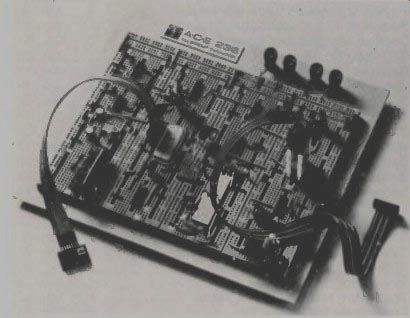
Figure 18A (above) Logic systems can be breadboarded easily by using
plug-in circuit boards such as this one from AP Products. (Courtesy of
AP Products)
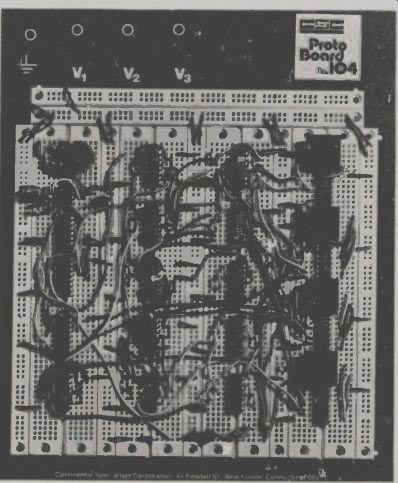
Figure 18B (at right) Another plug-in board for experiments is offered
by Continental Specialties. (Courtesy of Continental Specialties Corp.)
(adapted from: Electronic Servicing magazine, Jan. 1978)
Next: The Basics of Industrial Electronics, Part 8
Prev: The Basics of Industrial Electronics, Part 6