
By J. A. "Sam" Wilson, CET
Details are given for a simple digital test probe that you can build. To help you gain valuable experience using a probe and trouble shooting digital circuits, a hands-on experiment is described. The characteristics of NAND gates are explained.
Building A Probe (Experiment #1)
When you become experienced at troubleshooting digital problems, undoubtedly you will want a sophisticated logic probe. However, the probe of Figure 1 is adequate for studying the basic gates and other individual building blocks.
Power to light the LED comes from the digital gate that's being tested, and some logic circuits should not be loaded so heavily.
Later, we will describe another build-it-yourself probe which has lighter loading, and also we'll give the details of several commercial probes. For now, the Figure 1 probe will be satisfactory.
Typically, logic probes light to indicate a "high" or "logic 1" condition. Our simple probe does that, while remaining dark for a "low" or "logic 0" (or when not connected to the circuit). Test the probe by touching the +5-volt supply bus; the LED should light brightly.
Most logic probes include one or more LEDs as indicators (some light a different-color LED to indicate a "low"). Therefore, you should understand a few characteristics of LEDs.
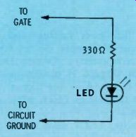
Figure 1 (at left) This simple circuit will indicate the logic state of
the gates discussed here.
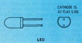
Figure 2 (at right) Most of the larger LEDs have a flat spot on the
plastic case that identifies the cathode lead. Some LEDs have a dot beside
the cathode wire, and the tiny ones intended to be mounted on a circuit
board might have the cathode bar symbol as part of the flat cathode lead.
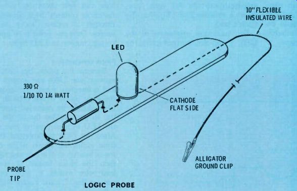
Figure 3 (above) A probe can be wired on a tongue-depressor or a piece
of plastic. The LED should be near the tip, and the wiring should be
insulated to prevent accidental shorts.

Figure 4 (at right) If you don't have a logic "breadboard," you
can prepare for the experiment of testing the NOT gates by connecting
a power supply to stiff bus wires.
LED characteristics
LEDs require less power than incandescent dial lamps do, they are available in several colors, and they light instantly. These features make LEDs a good choice for the indicators of logic probes.
Remember that Light-Emitting Diodes (LEDs) have some electrical characteristics of power-supply diodes. The reverse resistance is much higher than the forward resistance (however, both are higher than for common silicon diodes). When forward-bias DC voltage is applied, diodes attempt to maintain a constant voltage drop between anode and cathode. Above the threshold voltage, a small increase of forward bias results in a larger current increase. Diodes have some voltage-regulating action, and must be protected from overload by circuits that limit the maximum current.
LEDs also have similar voltage regulating characteristics, except the regulation centers around higher voltages.
Many LEDs are rated at 1.6 volts. If such an LED were connected from the +5 volts of a logic gate-to-ground, the LED would be grossly overloaded, and probably would fail rapidly. Therefore, a current-limiting resistor must be added in series with each LED. It's easy to calculate the value of this current-limiting resistor. LEDs are available in many different voltages and currents, but let's assume we have an LED rated at 1.6 volts and 20 milliamperes.
Subtract the 1.6 volts from the maximum voltage (5 volts). This leaves 3.4 volts for the resistor.
Dividing the 20 milliamperes (0.02 amperes) into the 3.4 volts, produces a resistance of 170 ohms (by Ohm's law). For maximum brightness of the LED, a 180-ohm resistor could be used. But lower voltages and currents provide longer life for LEDs.
So, I recommend a 330-ohm limiting resistor (Figure 1) to improve the safety factor. Also, the higher value allows the use of LEDs with other ratings.
Usually, LEDs have a flat side near the cathode pin (Figure 2); although, some have a colored dot beside the cathode lead, and a few seem to have no markings at all.
You can test them on an ohm meter, or connect them temporarily through a resistor to a voltage source. Only one polarity of applied voltage makes an LED light.
Probe construction Because the probe has only one resistor, one LED, one ground clip, and connecting wires, the layout of the logic probe is not critical. The LED should be mounted near the tip, so you can see the IC pin and the LED without moving your eyes.
Also, the LED is protected better from accidental shorts if the resistor is located at the extreme tip. In fact, the short length of resistor lead wire makes a good tip to contact the IC pins. Figure 3 shows a drawing of the probe.
No mounting board or case is necessary, except to protect against shorts, and to make the assembly more rigid (thus minimizing intermittent connections at the IC, and making the probe easier to handle). Some constructors attach the components to a wooden tongue-depressor. Others build the circuit inside a discarded pen case. Of course, some insulation (even plastic tape) should be provided.
A steady "high" applied to the probe causes maximum brightness of the LED, while a "low" does not allow any light. If the gate has pulses, the LED will have partial brightness or flash on and off, depending on the repetition rate.
Test the probe by connecting to the +5-volt supply. (See Figure 4 for the experiment setup).
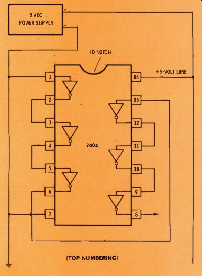
Figure 5 Wire the hex NOT gate IC as shown. Pin 1 is grounded, which
is equivalent to logic 0.
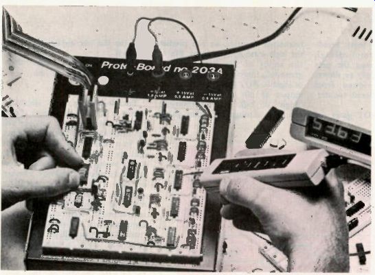
-------- Commercial prototype boards, complete with power supplies,
can be obtained from several manufacturers. (Courtesy of Continental
Specialties Corporation)

Figure 6 These are the logic levels of Figure 5, when drawn with the
gates arrange in a line.
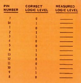
Figure 7 Record the results of your tests of the IC in Figure 5 at the
blanks of the right column. Then compare them with the expected results
in the center column.
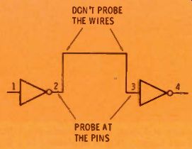
Figure 8 For the highest accuracy of digital tests, connect the logic
probe to the IC pins, and not to the circuit wiring.
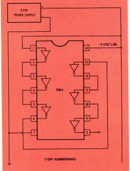
Figure 9 In the schematic of Figure 5, disconnect pin 1 from ground,
and connect it to the +5-volt supply. This is equivalent to a logic 1.

Figure 10 These are the logic levels in the circuit of Figure 9
Testing Hex NOT Gates (Experiment #2)
This experiment is intended to test all six NOT gates of a 7404 IC (Figure 5). Using a logic bread board (or point-to-point wiring), connect the IC between the pins and to the power supply as shown.
Remember: when viewed from above, ICs are numbered counter clockwise.
Since all of the NOT gates are connected in series, we can predict the logic state at each point. Pin 1, the input of the first gate, is grounded, therefore it has a "low" or logic 0. NOT gates invert, so the output at pin 2 should have a "high" or logic 1. This inversion continues through the other gates, with the last one having an output at pin 8.
Figure 6 shows the logic states with the gates drawn in line.
Troubleshooting gates
Troubleshooting any electronic circuit is done in two stages. First, you make a test; then, you analyze the results of that test. According to your knowledge, did the test indicate operation that is correct, totally wrong, or questionable? You see, no technician can know whether or not a circuit is operating correctly, unless he knows what results to expect from each test or measurement. And that's why a comprehensive knowledge of electronic theory should be the most important "tool" a technician can have.
The table in Figure 7 is for you to list the results of the logic measurements you made of the six NOT gates (right column). Compare your results with the ones you should have obtained, as they are shown in the middle column.
Probe the pins Make a habit of touching the logic probe to the pins of the IC, and not to other points of the same circuit. This will identify the location of any open circuits with better accuracy in less time.
For example, in Figure 8, you should find a logic level 1 at pin 2.
Also, the same logic level 1 should be found at pin 3. Therefore, if you measure a level 1 at pin 2, but none at pin 3, an open circuit must be between those two pins. But, if you measured a logic 0 somewhere along the wiring between pins 2 and 3, you would not know whether the first logic NOT gate was defective, or an open circuit was located between the test point and pin 2.
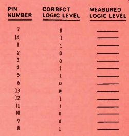
Figure 11 Record the logic levels of the second test of the NOT gates
(Figures 9 and 10) in the blanks of the right column. The correct results
are listed in the center column.
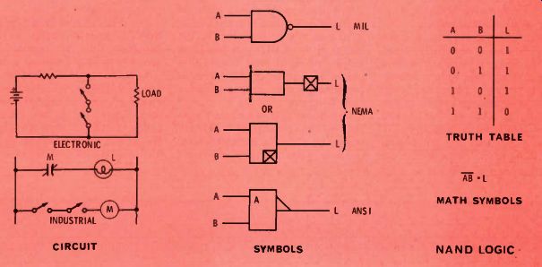
Figure 12 (above) These are the characteristics of NAND gates. You should
memorize the truth table and the math symbol.
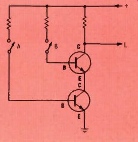
Figure 13 (at right) A NAND gate can be constructed from two bipolar
transistors wired in series between load resistor and ground. The transistors
can conduct only when both have forward bias (switches closed). Therefore,
when both inputs have logic 1, the output has logic 0.
Troubleshooting question #1
Assuming that all of the measurements recorded in Figure 7 were correct, with the second and third columns the same, have you completely checked the six NOT gates? (Answers for the questions are at the end of the article.) Testing NOT Gates, second part As shown in Figure 9, change the test circuit of the NOT gates (see Figure 5) by removing pin 1 from ground and connecting it to the +5-volt line. This places a logic 1 at pin 1; therefore, the output at pins 2 and 3 should be logic 0, from 4 should be logic 1, etc, until a logic 1 ("high") should be found at the last pin, number 8.
In other words, reversing the input logic level should reverse the logic levels of all the gates, as summarized in Figure 10.
The table of Figure 11 again provides a column for you to write in the results of your probe measurements of each NOT gate.
Troubleshooting question #2
After having completed the tables in Figures 7 and 11 and finding your results are correct, are you convinced now that each of the six logic gates is working properly?
Comments About The Experiments
These experiments have been written so you can merely "read through" them, if you don't want to perform them. You have a choice.
But, I strongly feel that such hands-on experience is very important to the overall "feel" and understanding of logic circuitry.
So far, you have learned how to construct a simple probe and to use it for making measurements of a typical IC package. You know now that a NOT gate should be checked with both "high" and "low" inputs to be certain one of the gates is not "hung up" at some level. You know that the probe will prove whether or not the DC supply voltage actually reaches the IC. These are not profound experiments, but they are important for the foundation of future work with logic circuitry.
NAND Logic NAND is the next basic gate to be analyzed. The word comes from a combination of NOT and AND, and that's a clue about the functions.
Figure 12 gives the four things about NAND gates that you should memorize: the schematic symbols; the truth table; the basic circuits; and the math symbol.
The truth table shows that the only way to obtain a 0 at the output is to have l's at both inputs. (Of course, if the NAND gate has three inputs, all three must have l's to obtain an output of 0.) All other combinations of inputs cause a logic 1 output.

Figure 14 If one input of a NAND gate is a logic 1 and the output is
logic 0, what is the logic state of the other input?
-------------
--------------
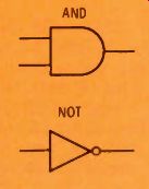
Figure 15 (at left) How can a NOT gate and an AND gate be connected
to form a NAND gate?

Figure 16 (below) A NAND gate can be obtained by adding a NOT gate to
the output of an AND gate.
Remember that the contact symbol in the industrial "ladder" schematic calls for normally-closed contacts, when the relay coil is not energized. When both switches are closed (logic 1), the contacts open (logic 0), and the load has no power (logic 0). Any other switch conditions (one or more low inputs) produce a logic 1 output.
The math symbol should be read: NOT A and B equals L. It is important that the overbar reach across both letters without a break.
A NAND gate made with two bipolar transistors is shown in Figure 13. When both switches are open (logic 0), neither transistor conducts (output logic 1). If only one switch is closed (logic 1, logic 0), one transistor is ready to conduct, but the other is open, so there is no current through them, and the output remains logic 1.
Only when BOTH switches are closed (logic 1, logic 1) can both transistors conduct, producing a logic 0 output.
Troubleshooting question #3
In the NAND gate of Figure 14 one of the inputs is at logic 1, and the output has logic 0. If the NAND gate is working properly, what must the probe indicate? Troubleshooting question #4 Figure 15 shows the MIL symbols for a NOT gate and an AND gate. How should these gates be connected to produce a NAND logic circuit?
Answers To Troubleshooting Questions
Answer #1 No, you have not checked the logic gates completely.
For example, suppose one of the gates is hung up so its output always is at logic 1. In that case, inputs of either logic 1 or logic 0 would not change the output logic 1. If the input has logic 0, you would believe incorrectly that the logic 1 output proves normal inversion operation; whereas, an input of logic 1 also would appear to produce a logic 1 output. For a total test, you must reverse the input logic state and verify that the output also reverses its state.
Answer #2 Yes, by making two tests, you now have verified correct operation of all logic gates. Not only must a certain input state produce the expected output state, but reversing the input state also must produce a reversed output state.
Answer #3 The logic probe should indicate logic 1 ("high"). The only way of obtaining an output of logic 0 from a NAND gate is to have logic 1 at both (or all) inputs.
Answer #4 Figure 16 shows how to connect an AND gate with a following NOT gate to obtain the performance of a NAND gate. This is an important concept, for it implies that you can connect together several basic gates to form other types of gates. For example, by using a sufficient number of NAND gates, you can construct any of the basic logic gates. In the same way, if you have enough NOR gates, any of the basic gates can be produced. In later articles, we will demonstrate this truth more thoroughly.
Next Month:
In the next article, I will show how NAND gates can be connected to produce the performance of other gates. Also, the basics of other logic gates will be discussed.
(adapted from: Electronic Servicing magazine, Feb. 1978)
Next: Part 8
Prev: The Basics of Industrial Electronics, Part 7
Also see: Sam Wilson's Technical Notebook