
The past several articles have explained digital logic circuits, including basic gates, truth tables, and typical circuits. This month, we will discuss some applications of digital logic.
Clocks
In logic systems, one of the land marks to look for is the clock-pulse generator. Many systems-especially those with counting circuits-use square waves or pulses to time the operations.

Figure 1. BASIC TRANSISTOR INVERTER: A transistor can function as a digital
NOT gate (inverter). Values of the two resistors must be chosen according
to the transistor and the application of the circuit.

Figure 2. A STABLE CIRCUIT: Two NOT gates connected in
this circuit are stable, although they accomplish nothing
The output at point D has the same digital waveform as the input at A. So, connecting them together does no harm, and does not change the operation
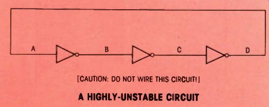
Figure 3. CAUTION: DO NOT WIRE THIS CIRCUIT! A HIGHLY-UNSTABLE CIRCUIT.
Three NOT gates in cascade become a strong and unstable oscillator because
of propagation delays. Refer to the text for details.
Multivibrators
Sometimes, the required clock pulses are obtained from multi vibrators. Digital multivibrators are quite different from the vertical or horizontal multivibrators used in TV receivers. Those multivibrators had two tubes or two transistors, with the output and inputs cross coupled, so each output fed the other input. The tubes or transistors were required to have gain, to compensate for the losses of the circuit. Digital gates have unity gain, since the input and output amplitudes usually are identical.
These facts alone show you that digital multivibrators must be different from those with transistors.
A transistor can operate as an inverter, as shown in Figure 1. A base high produces a low at the collector, and a low at the base causes a high at the collector.
When sufficient forward bias is present during the high and zero is applied during the low, the transistor either is saturated or cut off.
This is the characteristic of NOT gates. So, it follows that NOT gates can be wired as a multivibrator.
Stability without oscillation In Figure 2, two NOT gates are wired with each output feeding the other input. If these gates were transistors and a coupling capacitor is added, the circuit would oscillate.
However, with NOT gates, it is stable. A high input at A produces a low at points B and C, and a high at point D, which is connected back to the input. The feedback is redundant, but it can't increase the input any more than the originating high. (Two highs equal one high, in this case.) At the other extreme, a low at the input point A causes a low at B and C. and a low at D. which is coupled back to A. The signal fed back doesn't do anything, but it doesn't interfere. So, the circuit is stable. (Again, two lows at the input are no different from a single low.) Three NOTs become an oscillator When a third NOT gate is added to the circuit (Figure 3), it becomes highly unstable. At first look you might think that the circuit will merely turn itself off. A high at point A becomes a low at B, a high at C, and a low at D. But. D is connected to A, so it seems the low would cancel the original input high. However, an important characteristic, not one that shows on a schematic, modifies the situation.
Each gate has a propagation delay. That is, the output changes slightly later than the input.
Suppose a high is introduced to the input at point A. After a short time delay, the output at D becomes low, forcing the input low.
The new input low, following the time delay, produces an output high, which after a time delay becomes a low at the output, and so on continuously. The circuit is an oscillator, operating at a very high frequency! Of course, an external high is not necessary to trigger the oscillation. At turn on, all three gates have low inputs, and the first one to produce a high output starts the oscillation.
To reduce the frequency enough for clock operation, it is necessary only to lengthen the propagation time delay.
Improved multivibrator clock
In Figure 4, a capacitor has been added in parallel with the second NOT gate. It works in conjunction with the gate resistors to lengthen the time delay. (Actually, it is a time-constant oscillator.) The LED indicates the state of the output. R1 limits the LED voltage and current.
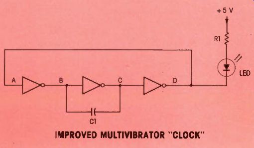
Figure 4 Adding a capacitance in parallel with the second NOT gate lowers
the frequency of oscillation. Any reasonable frequency can be obtained
by selection of the proper capacitance. The LED indicates an output signal.

Figure 5. For experiment #1, physically construct the three-NOT-gate
circuit of Figure 4 this way.
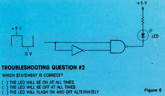
Figure 6.
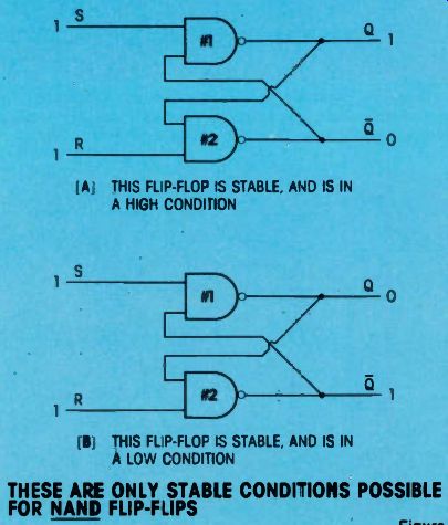
Figure 7.
Table 1 --- Flip Flop Possible Conditions
Experiment #1
Construct the electronic circuit of Figure 4. The corresponding physical layout using an IC is shown in Figure 5. A large capacitance (300 microfarad) slows down the free running frequency until the LED can be seen flashing on and off as it indicates the output state. Make sure to connect the cathode of the LED to the output at pin 8.
After observing the slow flashing of the LED, change the capacitance to 1 microfarad, and notice that the LED no longer appears to flash. Of course, the oscillator is operating at a higher frequency, and human eyes see this as a continuous glow.
While the capacitance is 1 microfarad, connect a scope to verify that the waveforms at points C and D are 180° out of phase. Use a dual trace scope, a single-trace scope with an electronic switch, or obtain a lissajous pattern to determine the phase.
Troubleshooting Question #1
In the circuit of Figure 4, will the LED be on (lit) when point D is high? Or will it be on when Point D is low? (Answers to the troubleshooting questions are at the end of this article.)
Troubleshooting Question #2
Figure 6 shows a square wave clock pulse that's fed to a simple logic circuit. Disregarding the possibility of "glitches" (from propagation delay), should the LED: (A) be on all of the time? (B) be off all of the time? (C) flash on and off periodically?
Cross-Coupled Gates
The next circuit for study has many different names, such as latch; cross-coupled gate; bounce less switch; R-S flip flop; and S-R flip flop.
The input terminals are marked S (for set) and R (for reset), and the output terminals are Q and NOT Q (Q). The output letters don't stand for anything specific, but are commonly used for the outputs of flip flops.
All flip flops have one characteristic in common. There are only two possible output states, and only one can occur at a time. These flip flop conditions are listed along with all of the various descriptions in Table 1.

Figure 8
These are the four steps for changing a NAND S-R flip flop from a low condition to a high condition.
Figure 7 shows an R-S flip flop made of NAND gates. The two input terminals (S and R) normally are in a logic 1 (high) state. The flip flop condition is changed by switching either S or R to logic level 0 momentarily. This circuit can be used only in applications where it is not possible for both inputs to have a logic level 0 at the same time.
Earlier in the series, we suggested that you memorize the truth tables for all of the basic gates. If you did that, you know the only way to obtain a logic level 0 at the output of a NAND gate is to have both inputs at logic level 1. Any other combination of inputs gives a logic 1 at the output.
The conditions of Figure 7 are the only two possible stable conditions. When the flip flop is switched from one condition to the other, the change is so rapid that it can be called instantaneous, for most applications.
In the high condition of Figure 7, there is a high from the S terminal to NAND #1, and a low input from the NOT Q terminal. This produces a high at the Q output terminal.
NAND #2 has two highs at the inputs. Therefore, the output is a low (logic level 0). In the low condition of Figure 7, NAND #1 has two highs at the inputs and a logic 0 (low) at the output. NAND #2 has a high and a low at the inputs, so its output is a high.
You always should verify the inputs and outputs of each gate for each of the conditions and changes discussed. That is good practice for solving troubleshooting problems.
Steps for NAND flip flops Figure 8 shows the four steps for setting a NAND flip flop from a low to a high condition. Step 1 shows the circuit in a stable low condition. In step 2, a logic 0 is delivered to the set terminal (the old input is shown in parentheses). Since the inputs now are a 1 and a 0, the Q output changes to a level 1
During step 3, the new logic 1 Q output of gate #1 is fed to NAND #2. NAND #2 now has two logic l's at the inputs, so the output at NOT Q becomes a logic 0. In step 4, the S terminal is returned to level 1. The flip flop now is in a stable high state. (In step 4, the Q output did not change because neither the previous low-and-low inputs of NAND #1, nor the new high-and low inputs can give a low output.
Therefore, the high state at Q remains the same when the set input receives the high at step 4.) Although considerable time is required to follow the step-by-step changes of Figure 8, the total time of the flip flop might be only a few nanoseconds.
Troubleshooting Question #3
Assuming that the NAND flip flop in step 4 of Figure 8 is stable in the high condition, what will happen if a logic 0 is delivered to the S terminal? The answer to Question 3 is very important. The rules that follow should help you understand some of the counting circuits which will be discussed later in this series.
They are:
Rule #1
If the NAND flip flop is in a low condition, it can be switched to a high condition by momentarily switching the set terminal to logic 0.
Rule #2
If the NAND flip flop is in a low condition, its output is not affected when a logic 0 is delivered to the reset terminal.
Rule #3
If the NAND flip flop is in a high condition, it can be switched to a low condition by momentarily switching the reset terminal to logic 0.
Rule #4
If the NAND flip flop is in a high condition, the output is not affected when a logic 0 is delivered to the set terminal.
Remember, when a flip flop is high, it is in the set condition. And when the flip flop is low, it is in the reset condition.
One more important factor is made clear by the steps of Figure 8 (particularly step 2). Switching from one condition to another takes place at the trailing edge of an input pulse. This is typical of NAND logic systems, such as TTL.
Troubleshooting Question #4
Which flip flops in Figure 9 will change, given the conditions shown?
Troubleshooting Question #5
In Figure 10 with the switch set to the A position, what will be the condition of the flip flop? No More Wiring Diagrams From this point on, the circuits for the experiments will be given, but the physical wiring diagrams will not be shown.
To obtain pin-out information for each IC, and how to determine which IC numbers have NANDs, NORs, NOTs, etc., I recommend you obtain either a TTL handbook or a copy of "TTL Cookbook" by Don Lancaster (Howard Sams book #21035). Keep in mind that an IC always must have a DC supply voltage before it can operate. Therefore, begin troubleshooting any problems you have with the experiments by checking for proper DC power.
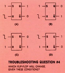
Figure 9---TROUBLESHOOTING QUESTION #4: WHICH FLIP-FLOP WILL CHANGE. GIVEN
THESE CONDITIONS'?
Experiment #2
Wire the cross-coupled gates of Figure 8. Begin by connecting both inputs (S and R) to the B+ to provide logic 1 inputs, but don't connect anything to the outputs.
Use a logic probe to determine the initial condition of the flip flop.
Next, change the condition of the flip flop by momentarily changing the wire of either the S or R input to common (ground). Make a list of which connections change the condition of the flip flop, and which connections have no effect.
Experiment #3
Wire the circuit of Figure 10, but before you apply the power, answer these questions:
(1) What condition should the flip flop have when the switch is at position A?
(2) What condition should the flip flop have when the switch is at position B?
Then, apply the power, try both positions, using a logic probe to verify your answers.

Figure 10—TROUBLESHOOTING QUESTION #5. WITH THE SWITCH POSITION SHOWN HERE,
WHAT WILL BE THE CONDITION OF THE FLIP-FLOP?
Answers for the Troubleshooting Questions
Answer #1 The LED will be on (lighted) when point D is low.
(When point D is high, the same voltage appears at each end of the LED.) Answer #2 The LED will be off at all times. The LED can light only if the NAND output is low. But, that's impossible because the inverter prevents the NAND inputs from ever having the same state.
Answer #3 Nothing will change.
The flip flop is in a high condition, so a logic 0 delivered to the S terminal will have no effect. Notice that a logic 0 at the S terminal will supply logic zeros to both inputs of flip flop #1. Since the output is level 0, it will remain there.
Answer #4 Flip flop A will change to a low condition. Flip flop B will not change. Flip flop C will switch to a high condition. Flip flop D will not change.
Answer #5 The flip flop will be in a high condition.
(adapted from: Electronic Servicing magazine, Apr. 1978)
Next: The Basics of Industrial Electronics, Part 11
Prev:
Also see: Sam Wilson's Technical Notebook