Many digital memory systems are built around flip flops, because flip flops easily can produce high and low digital states when needed, and then hold them indefinitely until changed by the programming. Several improved memories that use flip flops are described.
by Jack Webster
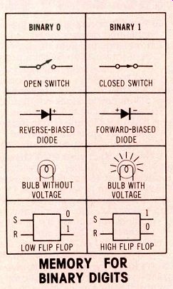
Figure 1---Memories can be constructed around any device which can attain
and sustain alternate on and off conditions. Of course, flip flops
are more compatible with digital circuits than the others are. MEMORY
FOR BINARY DIGITS
A typical microprocessor includes these subsystems: input and output devices; arithmetic-logic unit (ALU); control and timing-clock circuits; and two kinds of memory.
Each of these essential sections will be examined in detail. Then the interactions between individual sections in the microprocessor IC will be studied during the last parts of the series.
Memories use binary
Binary numbers in various combinations make up the language of microprocessors and computers. A single binary number (0 or 1) is called a bit (Binary digIT). Instructions to a microprocessor are groups of bits which are called words.
Any stable Memorizing a bit device that has only two states can be used as a memory. Each of the examples in Figure 1 has been used to some degree in computers. When such a device attains and sustains a desired digital state, that bit is said to be "memorized." Of the logic gates that are compatible with microprocessors, the most simple memory is the D latch of Figure 2. The output state is determined by the input data, and it's displayed by the LED.
A high input causes the flip flop to go high, thereby remembering a logic 1. Similarly, a low input forces the flip flop to remember a 0.
The Figure 2 circuit, however, has two disadvantages when used as a memory. When the flip flop is in the low condition, a transient noise pulse at the D terminal might switch the output to high momentarily. Also, the states are not stable unless the input bit stays at the D terminal. Otherwise, the flip flop will change when the input is removed (because inversion in the NOT resets the latch).
An improved memory Figure 3 shows an improved memory flip flop (or latch). The quiescent inputs to a NOR flip flop (when it's not being switched) are two logic zeros. A logic 1 applied to the S terminal switches the flip flop to high. This state is stable, and the high remains even after the logic 1 at the S terminal is removed. A logic 1 applied to the R terminal then switches the flip flop output to a low condition. The flip flop remains low after the R terminal is pulled low; this too is a stable condition.
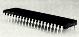
---------- Type 8080 microprocessor has a 40-pin DIP case, and it
includes flip flop memories.

Figure 2 --- A D-latch output follows the state of the input signal. however, it cannot maintain the last digital state after the input signal
is removed. D-LATCH MEMORIZES BINARY DIGITS
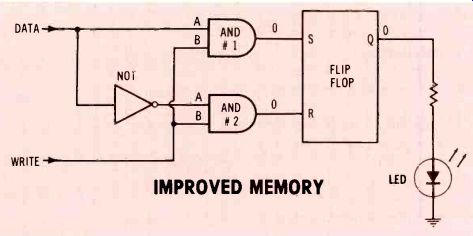
Figure 3 --- An improved memory allows the last state of the flip flop
to be retained after the data signal is gone. The AND gates also prevent
any change of flip flop output state unless the "write" input
has a high. IMPROVED MEMORY

Figure 4 --- Two of Figure 3's four possible input conditions are illustrated.
(A) A high at both inputs produces a high at the output LED. (B) A high
at the write input and a low at the data input produces a low at the
output LED. If the write in put has a low, H freezes the memory and the
flip flop output state cannot change, regardless of the state at the
data input. HIGHS AT BOTH INPUTS PRODUCES A HIGH OUTPUT; A LOW INPUT
PRODUCES A LOW OUTPUT
The NOR type of flip flop must not have highs at both S and R inputs simultaneously-a requirement which is fulfilled by two AND gates and the NOT that inverts the state at the A input of the bottom AND gate.
Because of the NOT gate, the A inputs of both AND’s always will have opposite logic states. The B inputs are tied together and are connected to the "write" input.
AND gates require highs (logic ones) at both inputs before the output can go high. Therefore, when the write input has a logic 1 and the data input has a digital signal, one of the two AND gates will have a high output. A high from AND 1 activates the S terminal, causing a high condition of the flip flop. A high from AND 2 activates the R terminal, switching the flip flop to the low condition, as described before.
These important functions are illustrated in Figure 4. Both the data and write inputs of Figure 4A have highs. Therefore, AND 1 has highs at both inputs, and the output consequently goes high which places that high at the S input of the flip flop, forcing it to produce a high output. At the same time, AND 2 has a low input from the NOT and a high input from the write terminal. These conditions produce a low AND 2 output.
The data input of Figure 4B has a low while the write input has a high. Therefore, AND 1 has one high input and one low input which produces a low output. At the same time, AND 2 has highs at both inputs (the NOT has inverted the data-input low to a high), so its output becomes high which switches the flip flop R input (and the flip flop output) to low.
A low at the write input prevents either AND from producing an output high. In turn, this condition stops the flip flop from changing to a different logic state. In other words, a low at the write terminal freezes the flip flop memory.
Reading the memory
The Figure 3 circuit would be more flexible and useful if the output state could be "read" or observed at any designated time.
For example, suppose 10 of these memories are operating but only the output of the fifth one is to be delivered somewhere at a certain time.
Addition of AND gate 3 (Figure 5) allows the flip flop output state to be observed only when desired. If the flip flop Q output is high and then a high is applied to the "read" input, AND 3 produces an output high which lights the LED. When the read input has a logic 0, the AND 3 cannot have a high output and the LED doesn't light.
Basics of memory
These are the basic requirements for digital memories:
The digital circuit must have only two stable states which can be sustained indefinitely;
Data can be stored (memorized) only after a command to "write;" and
The stored data must be displayed by command from the proper "read" signal.
Types of memories
After the data has been entered into the flip flop memory by application of a logic 1 to the write terminal, the data logic state is maintained without any more actions being required. The data remains unchanged so long as supply-voltage power is delivered to the gates and the flip flop. This type is called a static memory.
Some memories require constant refreshment to maintain the data.
They are called dynamic memories.
If the data is lost when the power is turned off, it's called a volatile memory. A non-volatile memory retains the data through any number of power on/off cycles.
A few examples should help clarify these terms and concepts.
Dynamic memory---A dynamic memory model is shown in Figure 6. A positive input pulse charges the capacitor which retains the charge for a time to produce a logic 1 digital level at the output. The stored information would be lost, however, without the recirculation circuit which periodically replenishes the charge.
Of course, remember this is only a simple model of a dynamic memory. Real memories are not constructed this way, although the charge in a capacitor has been used as a memory in some commercial equipment.
Data latch---Figure 7 gives the pinout for a type 7475 data latch; and the truth table in Table 1 applies to each of the D-type flip flops in the IC. The top row (first under the line) shows that when the data input (D) has a low when the gate (write) terminal has a high, then the Q output develops a low.
(Of course, the Q output state always is opposite to that of the Q output.) Row number 2 shows that a logic 1 at the data-input terminal (D) produces a logic 1 at the Q terminal when the G (gate) input is high. And the bottom row shows that when the gate (G) input is low, the Q output will not change regardless of a high or a low at the data (D) input.
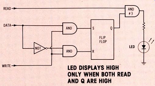
Figure 5---Addition of a third AND, and a "read" input allows
the flip flop to change state (as in Figure 4), but with the LED showing
a high only when both the read input and the flip flop Q output have
highs. A low at the read input allows data to be stored, but without
any readout of the state of the bit. LED DISPLAYS HIGH ONLY WHEN BOTH
READ AND CI ARE HIGH

Figure 6 Digital dynamic memories (which require periodic refreshing)
are not constructed as shown here. But the diagram shows how a stored
high leaks away unless it is continually refreshed by the regeneration
circuit.
DATA LATCH TRUTH TABLE
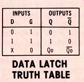
Table 1 This is the truth table for each data latch of Figure 7.
DYNAMIC MEMORY MODEL
The data latch is useful for holding a number on display. For example, a frequency counter works by actually counting the number of cycles that occur during a precise time period. The number at the end of the count needs to be displayed while the next count is going on. A data latch with the gate (write) pulled low freezes the data (count in this case) until a high is applied to the gate when an updated count is needed.
A frequency-counter block diagram is shown in Figure 8. Of course, additional 7-segment displays are required for counts of more than nine.
Data latches are used often in IC memory arrays. A typical array might have 16 rows of D flip flops with four in each row (for 64 flip flops). When a bit of information is to be stored or retrieved, one of the 64 flip flops must be located.
The method of locating one certain flip flop is similar to that used with many maps. It's done by specifying a column and a row.
Newville in Figure 9 is located at B3.
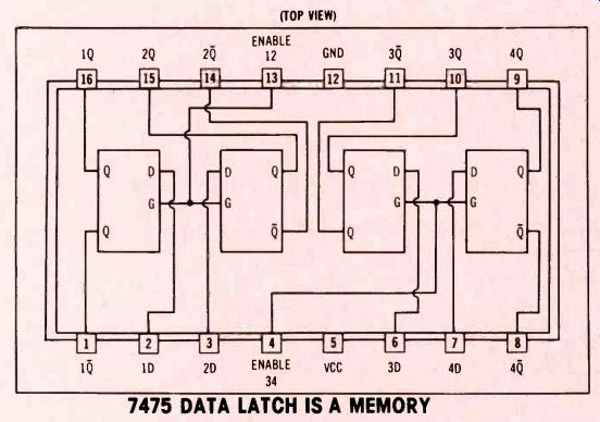
Figure 7---A data latch is a type of memory. Four data latches are included
in each 7475 IC. 7475 DATA LATCH IS A MEMORY
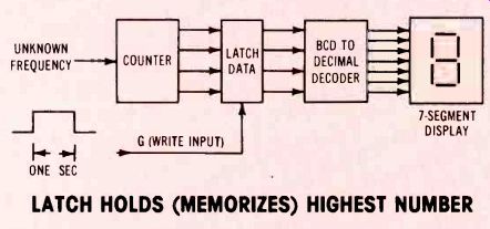
Figure 8 -- A latch holds a digital number, and it can be used in a frequency
counter to display only the final tally. LATCH HOLDS (MEMORIZES) HIGHEST
NUMBER
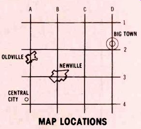
Figure
9---Locations of digital bits are accounted for by a system similar to
that used with maps. Vertical lines equal digital columns and horizontal
map lines are equivalent to digital rows. MAP LOCATIONS
Integrated-circuit memory
Figure 10 is a block diagram of an IC memory that's similar to those in microprocessors. There are 32 horizontal rows and 32 vertical columns, making a total of 1024 locations for the storing of data.
Some of the terms might be unfamiliar. For example, the symbol R/W means "read, but do not write." The symbol CE stands for "chip enable," and the terminal must be activated with a logic low before information can be brought into or out of the memory.
Access to the row that has a certain memory cell is obtained by application of the proper binary number to terminals A0 through A4. Similarly, the correct column is located by applying a binary number of terminals A5 through A9.
For example, to locate a memory cell that is in the fifth row and first column, the logic levels of Table 2 must be applied. At the same time these logic levels are applied to the address terminals, it's also necessary to apply the proper signal to the chip enable (CE) terminal. Or, if information is being retrieved, the read-but-not-write terminal also must be activated.
The truth table of Table 3 is supplied by National Semiconductor for the Figure 10 memory. It allows information to be inserted or retrieved from the memory.
First row of the truth table shows that the IC is inoperative when the CE has a logic 1 (high) applied.
The second row indicates logic 0 will be stored in the memory when CE, R/W and D(in) all are at logic 0. The specific cell where the logic 0 is stored is selected by terminals A0 through A9. The D (out) terminal is for output logic, so signals are not applied to it. However, D(out) will have a logic level 0 output at this time.
The truth table third row specifies that when CE and R/W are at logic 0 and D(in) is at logic 1, a logic 1 is stored in the cell which has been selected by terminals A0 through A9.
Fourth row of the truth table shows that the stored data can be retrieved by making the CE terminal low and the R/W terminal high. The data appears at the D(out) terminal. As before, the terminals A0 through A9 must be programmed to select the specific cell from where the stored information is to be retrieved.
Microprocessor memory
Memory blocks in microprocessors are similar to the one de scribed. However, a special coded signal is used to locate a memory cell.
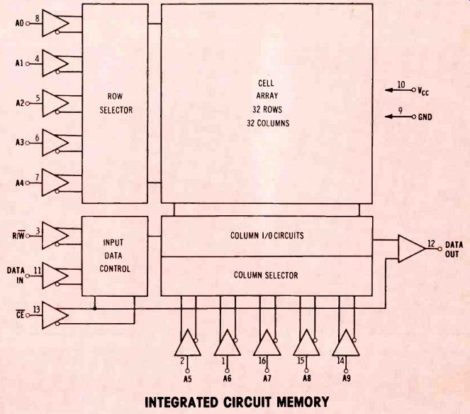
Figure 10---A block diagram of an integrated circuit memory shows the
access points to the rows and columns. INTEGRATED CIRCUIT MEMORY

Table 2---To locate a memory cell in the fifth row and the first column,
these logic levels must be applied to the Figure 10 memory. LOCATING
A MEMORY CELL

Table 3---These logic levels are required to move information into and
out of the Figure 10 memory. MEMORY TRUTH TABLE
Also see: Selecting replacement resistors