CTC99 & CTC101
Remaining coverage of the RCA SCR-regulator operation is presented first. Then the master/horizontal oscillator and other stages inside IC U400 are analyzed.
By Gill Grieshaber, CET
Regulation of the +123V supply is enhanced by two separate actions. A dc voltage of +155V and negative-going pulses are present at the SCR anode. Variable power to maintain a constant +123V regard less of load or line-voltage changes comes from automatic changes of the SCR conduction time (produced by four transistors in the regulator circuit). The pulses are included to unlatch the SCR during each retrace. However, the first half of each pulse is rectified by the SCR (silicon controlled diode), and this extra boost of power adds a non-varying contribution to the +123V-supply voltage.
Detailed regulation operation
Complete understanding of the 123V regulator requires an extensive analysis of dc waveforms at each point of the circuit. These waveforms also should show the zero-voltage line and the +33V supply line. Especially important are the dc waveforms from base to emitter. Such an analysis was made, but only a few of those waveforms will be presented in a condensed discussion.
Oscillator frequency control--The emitter of Q102 is connected to the +33V supply and the base receives a sample of the regulated (123V supply) voltage through the R116/ R117 voltage divider. Several resistors (pictured in the upper left corner of Figure 1 were clipped out during calibration at the factory to make up the precise value of the voltage divider top leg. There is no adjustable control, as shown in the complete schematic of Figure 2.
Because the emitter has a fixed voltage, the forward bias of PNP Q102 is in proportion to the regulated voltage. It is possible to analyze according to bias and its corresponding affect on collector voltage. For example, a higher regulated voltage provides lower forward bias to PNP Q102, which in turn decreases the C/E current.
For a PNP transistor, the positive supply enters at the emitter. There fore, the plate voltage becomes less positive. Such a method is accurate, but slow and complicated.
It's easier (and sufficient) to consider that the collector change always is opposite to the base change. A positive-going base produces a negative-going collector, and a negative-going base produces a positive-going collector.
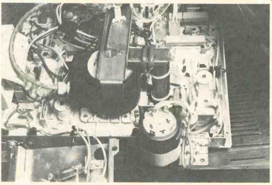
---------- All 123V regulator components are located in front of the flyback;
at the right in this picture taken from the high-voltage side.
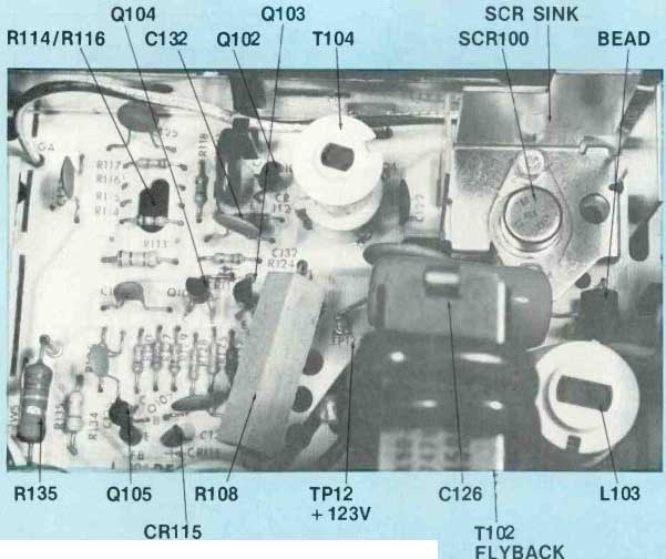
Figure 1 Arrows point to major components of the regulated +123 supply.
Therefore, an increase of the regulated voltage causes this sequence: a positive-going Q102 base; a negative-going Q102 collector; a negative-going Q103 base; and a positive-going Q103 collector.
Q103 collector current charges C132, so a higher regulated voltage places a higher positive voltage at the active end of C132 (the other end connects to the +33V supply).
This charges C132 at a slower rate, thus delaying the start of SCR conduction, and the regulated voltage decreases to the desired value.
It seems wrong that a higher positive voltage applied to the variable-voltage end of C132 represents a lower charge. That's be cause one end of the time-constant capacitor usually is grounded, but this circuit applies +33V to the non-varying end. Remember, a charged capacitor has full supply voltage across it (maximum voltage) while an uncharged capacitor has the same voltage at both ends.
Therefore, if the varying end has +33V and the fixed end has +33V, the capacitor is discharged completely. (In conventional circuits, both ends would have zero volts when discharged.) Notice, however, that Q104 is triggered when its emitter voltage (which is clamped by CR113 to the C132 voltage) decreases to a critical point about 0.6V below the instantaneous base voltage (see the Figure 2 waveforms). But, none of this is possible unless Q105 previously was conductive during the horizontal-retrace time. Triggering of Q104 will be explained more thoroughly after the Q105 operation is clarified.
Q105 conducts twice-Regulator action is synchronized to the horizontal sweep by applying a negative-going flyback pulse to the Q105 base during retrace. The resulting Q105 conduction discharges C132 which starts the regulator timing operation. (Q104 and the oscillator function is not used here, although Q104 conducts slightly.) A small triggering pulse reaches the SCR gate, but the SCR is being un latched by the negative-going anode pulse, so it is ignored.
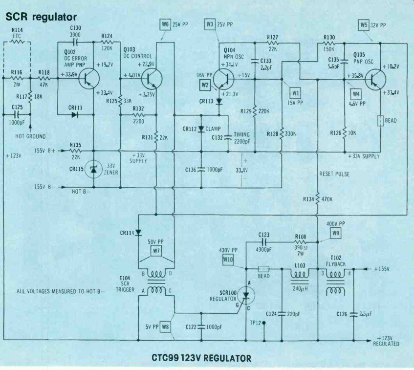
--------- SCR regulator; CTC99 123V REGULATOR
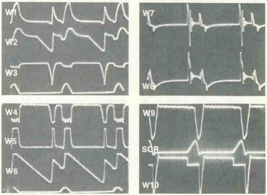
Figure 2 This is a complete schematic of the + 123V regulated supply.
The brightness was turned down to stabilize the circuit action. Therefore,
the voltages and waveforms will be slightly different when tested with
a normal picture.
The sole purpose of this Q105 conduction is to bleed C132 completely so it can be charged according to the Q103 collector current. Notice that Q103 has no resistive dc path to B+. Instead, that end of C132 has +33V following the discharge by Q105, and the Q103 collector current is the charging current of C132.
Unless a flyback pulse or an oscillation pulse from Q104 reaches the Q105 base, Q105 has insufficient bias for any collector current.
Therefore, the Q105 base and emitter waveforms are pulses (see W4 and W5 in Figure 2).
Emitter triggered Q104--The situation is completely different for Q104. 8129 and R128 supply a fixed amount of positive voltage to the Q104 base (in waveform W1 of Figure 2, this appears as a base line). But for most of each cycle, the 0104 emitter is more positive than the base (which is reversed bias) and Q104 cannot conduct.
First, conduction occurs when the emitter voltage (W2 in Figure 2) drops slightly below the base voltage, thus producing forward bias.
When Q104 receives a small forward bias, it conducts to apply a small negative-going signal to the Q105 base. In turn, Q105 conducts and applies a positive-going signal to the Q104 base. Both signals are forward bias for the respective NPN and PNP transistors. The effect is regenerative, going to saturation in a short period of time. Finally, C132 is drained and Q105 current stops. This starts a degenerative action which quickly forces the Q104 emitter more positive than its base. Thus, Q104 current stops also.

Figure 3---Two dc-voltage lines on the SCR-anode waveform help clarify
operation of the regulator SCR. The upper horizontal line marks the average
voltage of the waveform. However, + 155V is fed to the circuit, thus
the line represents the + 155V supply. The single stair-step below the
line is the regulated + 123V supply voltage. It appears at the SCR anode
because the anode and cathode are shorted together during SCR conduction.
(This stair-step moves to the left when a higher voltage is needed.)
Because of the + 155V supply, the true zero-voltage line is moved down
to the approximate center of the pulses (lower line).
Now C132 begins to charge again from the Q103 collector current, and a partial charge is built up before a negative-going flyback pulse reaches the Q105 base and discharges it. This is slightly more than one horizontal scanning line.
Of course, the Q105 current pulse triggered the SCR into conduction to replenish the +123V supply at the proper time according to the operation of Q102 and Q103 that slowly charge C132.
All Figure 2 waveforms show slightly more than two horizontal lines, and several pictures have horizontal flyback pulses which establish the beginning of each scanning line.
Operation of L103
If the flyback pulses and hot-supply dc voltage were connected to the SCR100 anode without going through inductance L103, those pulses would be applied directly to filter capacitor C126 when the SCR conducted. Clearly, this would rep resent an ac short across the flyback, and it would kill the high voltage.
Therefore, L103 is included to serve as a low-loss decoupling between the flyback pulses and the filter capacitor. Also, it slows down both the increase and decrease of SCR current (see W10 in Figure 2).
Rectifying negative pulses
W9 waveform in Figure 2 show 400VPP negative-going pulses that are fed from the flyback to L103 and then to the anode of SCR100.
At first, it seems impossible for the SCR to rectify negative pulses. But these are not dc pulses; therefore, the positive peak can be rectified.
Also, the inserted +155V supply moves the zero line down to increase the positive-peak amplitude and the rectified voltage.
The peculiar SCR anode wave form in W11 is not easy to understand until the various dc levels are identified as shown in Figure 3. The horizontal line at the top is the average voltage of the waveform; however, +155V is added to it, so the line represents +155V. Just below it is a stairstep of +123V which is present at both anode and cathode of SCR100 during conduction. Then, the horizontal line near the vertical center of the waveform is the true zero line. The left half of the large pulse is decoupled from the flyback by s L103, and during conduction, no pulse is there because filter 0126 has removed it. Therefore, the SCR current continues after the start of the flyback pulse (although at a decreasing rate) until the input pulse drops to the zero line. There the SCR unlatches, and all conduction current (both +155V and pulse) ceases. This explains the rectification of pulses that appear to be too negative to allow rectification.
Notice that the +123V step is taller (higher voltage) at the end of conduction following the pulse rectification. Also, the SCR on time is about 25%. Therefore, without the dc from pulse rectification, the regulated voltage would be about +40V and not +123V. This extra supply voltage provides excellent regulation at low line voltages.
Regulation versus line voltage
The multiple scope traces of Figure 4 compare the waveforms at line voltages of 120Vac (picture A) and 60Vac (picture B). Lower line voltage reduced both flyback and SCR pulses by about 25%, and the step between supply and regulated voltages almost disappeared.
The 120V SCR on-time of about 25% lengthened to about 50% at 60Vac. These waveforms were made when the raster was black. With a normal picture, the regulator step moves sideways (in response to the varying CRT current) and blurs the waveform.
Attempts were made by varying both brightness levels and line voltage to move the step (that shows start of SCR conduction) farther to the left (thus increasing conduction time), but without success. Evidently this approximate 50% duty cycle is the maximum permitted by the design.
As a test of the regulation, the line voltage was varied and the following figures obtained:
LINE +155V +123V
125 163.4 123.6 120 156.1 123.4 115 147.7 123.3 110 141.3 123.1 105 134.2 123.0 100 126.7 122.9 95 119.6 122.7 90 112.0 122.1 85 104.7 121.2 80 99.0 118.5 75 91.6 112.9 70 85.4 105.5 65 80.1 99.2
Notice that the regulated voltage was higher than the source (155V supply) voltage for all line voltages of less than 100Vac. This is better than perfect regulation (in one sense', and it is possible only because of pulse rectification.
No visible narrowing of picture occurred until the line voltage dropped to below 85Vac. Some slight narrowing was noticed at about 80V, and below 70V hum bars and retrace lines could be seen.
One limitation was discovered about operation at low line voltages.
If the TV was operated first at normal voltages and then the line voltage was reduced, it would operate (with some hum bars and a loss of width) at less than 60 line volts. But if the TV was turned off for a time and then turned on at the low line voltage, the start-up circuit did not work. Therefore, the TV would not operate until the voltage was increased above about 90V.
One of the troubleshooting techniques that will be described later makes good use of this ability to show a picture with low supply voltages. The source voltage is supplied through a resistor that limits damage from overloads, and a positive voltage is applied to TP13 (between CR421 and CR422) to start the oscillator, which drives the output transistor and produces some HV and width.
Horizontal frequency The CTC99 and CTC101 chassis employ a single IC (U400) to produce both horizontal and vertical sweep frequencies from a single master oscillator and a series of dividers.
Frequency of this master oscillator is not 15.734Hz, but must be twice that frequency. For interlaced scanning, each vertical color field must have 262.5 horizontal lines.
But dividers cannot produce a half line, so the master oscillator is operated at 31.468kHz which provides the required 59.94Hz vertical-field rate when divided by 525 lines.
From the 31.468kHz master oscillator frequency, it is necessary only to divide by two to obtain the correct 15.734kHz horizontal line rate.
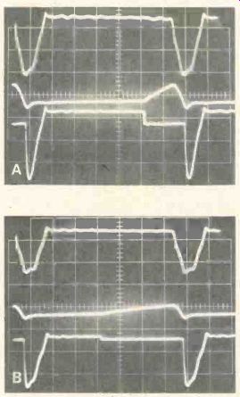
Figure 4 (A) These are the normal flyback pulses (top trace), SCR anode
current (center), and SCR-anode wave form (bottom trace) when the raster
was black and the line voltage was 120Vac. The scope controls were not
adjusted, but line-voltage reduction to 60Vac produced the changed wave
forms of (B).
Top trace shows the + 123V regulated supply's 6VPP ripple, while the horizontal-sweep waveform is included below to show timing of the ripple.
(A) Because of the CRT socket and a maze of wires, the U400 horizontal-oscillator (and vertical-countdown) IC is not visible. (B) After wires and components are moved, U400 can be seen. It is a 14-pin DIP IC on the circuit board under the right side of the picture-tube socket/board.

Figure 5---Waveforms and voltages are included with this complete schematic
of the CTC99 horizontal phase-detector and oscillator. The master oscillator
frequency is twice that needed for the horizontal sweep.

Figure 6---This is a sequence showing the anti-bend waveforms. (A) Top
trace shows the horizontal pulses brought to R456 in Figure 5 (waveform
W6). The bottom trace shows sawteeth at CR428 anode (formed by R456 and
C438 from the pulses). (B) Most of the top trace is 31,468Hz sawteeth
from the master oscillator, but dents in alternate cycles are ripple
from CR428 cathode. Bottom trace shows the master oscillator sawteeth
(W7 in Figure 5) at pin 12 of U400.
Tiny dents in alternate sawteeth show effects of the anti-bend action.
Figure 5 shows the complete schematic of the progression from composite video to sync, to the locked 31.468kHz master oscillator, the divide-by-two and the internal buffer stage. The vertical count down stages are in the same IC, but they are described later.
The phase detector requires differentiated horizontal-sync pulses at pin 3 (W4 waveform) and a sawtooth horizontal signal (W5) at pin 14. This is the conventional type of phase detection. However, notice that both sync and feedback signals operated at the 15.734kHz horizontal rate, but the error-correction control voltage at pin 1 is brought to pin 12 where it controls the frequency of the 31.468kHz master oscillator. In other words, the operation is like that of a phase-locked loop (PLL) with phase detector and oscillator operating at different frequencies.
Another similarity to the PLL is that the oscillator is voltage tuned, and without any sort of tuned circuit. Only pulses and square waves are needed, so a tuned circuit would be superfluous.
Oscillator locking
Locking of the master oscillator is accomplished by combining the phase-detector correction variable-dc voltage (from pin 1) with a manually adjusted dc voltage from the horizontal-frequency control (R449).
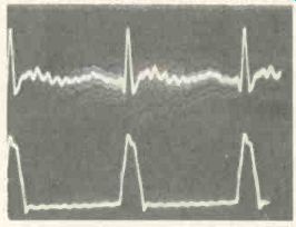
Figure 7--Narrow 0.25VPP pulses (top trace) are found at the U400 pin-1
correction voltage that locks the master oscillator. Lower trace shows
normal flyback pulses for comparison.
For locking adjustments, the sync is removed by grounding TP10, and the free-running frequency is adjusted for zero-beat with a station picture by rotation of R449. Then the short is removed from the sync.
That's all; there are no stabilizing or additional adjustments.
When the picture was locked correctly to a station picture, the sweep frequency measured 15,734.3Hz. With TP10 grounded, it was 15,775Hz, and when the TV was changed to an unused channel, the frequency measured 15,738Hz.
Those figures show excellent oscillator operation.
Anti-bend Bending at top of the raster is prevented by applying filtered horizontal pulses to the oscillator. First, the pulses are integrated into sawteeth by 8456 and C438, then peak rectified by CR428, and finally the ripple from rectification is applied through C436 to the oscillator voltage at pin 12. Figure 6 shows the waveform sequence.
When diode CR428 was shorted as a test, a crosshatch showed several narrow horizontal bands of displacement that moved up slowly through the raster. These bands were not very noticeable on station pictures, but the stability was affected slightly.
VCRs vs. weak-signal stability
As these TVs come from the factory, the component values provide fast correction of oscillator frequency. This is necessary for stable operation with videocassette tape recorders.
If excessive snow or strong local noise sources produce unstable pictures, the time constant can be changed by removal of resistor R425 and capacitor C447 (at the bottom of Figure 5 schematic), and shorting stake TC to stake TC1.
Figure 7 shows the small-amplitude waveform that appears at the error voltage (U400 pin 1). The amplitude is reduced by the time-constant change.
Duty cycle and divider
Downstream of the master oscillator inside U400 is a stage called duty cycle, which provides the desired waveform for driving the divide-by-two stage that follows.
The dc voltage at pin 13 is critical for generation of the correct duty cycle. Therefore, the voltage divider resistors R453 and R452 have 1% and 2% tolerances.
Output signal from the divider drives the internal buffer, and its square-wave output goes from pin 10 through R464 to the base of transistor Q406 buffer. In turn, Q406 output feeds the horizontal driver and it drives the base of the horizontal-output transistor.
Next month
Details, voltages and waveforms of the horizontal buffer, driver, and output stages will be presented next month. Power supply and horizontal troubleshooting methods will be combined after the circuit analysis is completed.
Also see: Calculating service labor rates