001 AUDIO-CONTROLLED MAINS SWITCH
It is often useful for audio or video equipment to be switched off automatically after there has been no input signal for a while.
The function of the on-off switch in such equipment is then taken over by switch S2 in the accompanying diagram. It remains, however, possible to switch off manually by means of S1. Automatic switch-off occurs after there has been no input signal for about 2 minutes: this delay makes it possible for a new record or cassette to be placed in the relevant machine.
The audio input to the proposed circuit may be taken from the output of the relevant TV set, amplifier, or whatever. The input earth is held at +6 V with respect to the circuit earth by potential divider R1-R2-R3-R4. The two 741s function as comparators: the output of IC1 goes high when the in put signal is greater than + 50 my, whereas the output of IC2 goes high when the input signal becomes more negative than -50 mV. Resistors R6, R7, and Rs form an OR gate that drives transistor Ti. If the output of either IC1 or IC2 is logic 1, T1 conducts.
The 555 operates as a retriggerable monostable, whose period is determined by Rio and C1. The device is triggered when its pin 2 is earthed by the closing of S2. Its output, pin 3, then remains high for 1 to 2 minutes, depending on the leakage current of the 555. The monostable resets itself as soon as the potential across C1 exceeds a certain value.
As long as there is an input signal to the circuit, T1 conducts and C1 remains uncharged. As soon as the audio signal ceases, T1 switches off, and C1 charges until the potential across it is sufficient to reset the 555. The monostable may also be reset by closing Si, which connects pin 6 of the 555 to +12 V.
When IC3 is reset, C1 is discharged via its pin 7.
Resistor Rn serves as protection, because without it T1 could short-circuit the supply lines.
When the output of IC3 goes high, T2 conducts, the relay is energized, and the relay contacts switch on the mains voltage as appropriate. To counter the induced potential when the relay contacts close, which could damage T2, diode D1 has been connected in parallel with the relay coil.

002 AUDIO LINE DRIVER
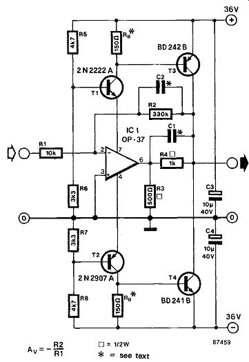
Integrated operational amplifiers are not always suitable for applications where a high signal level (1J0:510 V.) is required for driving a relatively low impedance (Z=50-600 ohm). The amplifier de scribed here is eminently suitable as a high dynamic range line driver or power buffer in public address systems and AF distribution amplifiers.
The input amplifier of the line driver is formed by a low noise opamp
Type OP-37 from PMI.
This ensures the following technical specification of the line driver: U0=70 Vpp max.; 10=400 m App max.; D_tot =0.01% at U0=10 Vrms, ZL = 50 ohm and S/N 90 dB.
Regulators T1-T2 bring the supply voltage for the OP-37 down to ± 15 V. The complementary power output stage is formed by T3-T4 The amplifier has a standard negative feedback circuit R1-R2, which results in a voltage gain A, = -(R2/R1). A local feedback R3-R4 has been included to keep the output voltage of the opamp within safe limits, while capacitors C1-C2 serve to improve the stability. It should be noted that the value of C1 and C2 depends on the construction of the line driver: typical values are 680 pF for C1 and 22 pF for C2.
In a prototype of the circuit, neither capacitor was required for the frequency response to remain flat ( ± 1 dB) up to 100 kHz.
Resistors
Re should drop just enough voltage for T3 and T4 to start conducting (class A-B operation).
The quiescent current of IC, is about 3 mA, so that 150 ohm can be taken as a suitable starting value for Re. The quiescent current in the power output stage should be between 20 and 50 mA. Higher values of Re cause the quiescent current, and hence the power dissipation, to increase, resulting in less distortion. The power output stage is not protected against thermal overloading, so that due dare should be taken in adjusting the quiescent current.
003 AUDIO TRANSFER EQUALIZER
Limiting the bandwidth of an audio system to 20 kHz affects the behavior of the system in the pass band. The steeper the filter characteristic, the greater the phase shift in the pass band. That phase shift stands in non-linear relation to the frequency, and this causes a frequency-dependent delay of the signals (increasing with frequency from about 4 .. .6 kHz). This effect is audible.
The CD (compact disc) player is an example of a system in which the bandwidth has been so limited.
Particularly the Sony CD player and its clones suffer from a frequency-dependent transfer time. The Philips (and Philips-derived) system does not suffer from this effect.
The effect can be negated by introducing a delay in the transfer time of the frequencies below 4 . . .6 kHz, which equalizes the delay over virtually the entire audio range. In other words, transfer of all audio frequencies is carried out at the same speed as it should.
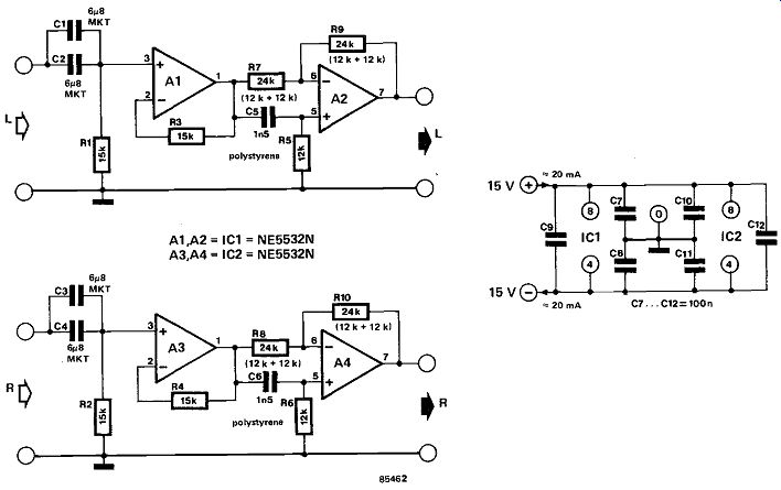
Such a delay is realized by phase shifter A2 (left hand channel) and A4 (right-hand channel) in the accompanying figure. The maximum delay for the lowest frequencies is 2R5C5 = 2R6C6 = 36 f4s.
The circuit is connected between the output of the CD player and the AUX or CD input of the main amplifier.
004 COMPRESSOR
This versatile circuit serves to raise the average output power of an AF amplifier. Its simplicity makes it suitable for applications in intercom systems, public address and discotheque equipment, and also in various types of transmitter.
Compression of music and speech essentially entails reducing to some extent the dynamic range of the AF input spectrum in order to drive an AF power amplifier with a fairly steady signal level just below the overload margin, thus increasing the average output power of the system. However, some distortion is inevitably incurred in the process of amplifying the relatively quiet input sounds and attenuating the louder sounds. It is evident, therefore, that the control of the amplifier/attenuator function in the compressor determines to a large extent just how much distortion is introduced by the circuit.
Before inserting any type of compressor in an AF signal path, due consideration should be given to the attack time i.e., the time it takes the circuit to detect and counteract a sudden increase in the amplitude of the incoming signal. Allowing for personal preference and the character of the input signal (speech, popular music, etc.), the attack time of a compressor generally lies in the range from 0.5 to 5 ms. The release time of the compressor is the time it takes the circuit to return to the settings that existed before the rise in amplitude occurred. Contrary to the attack time, the release time is usually of the order of seconds. If it is made too short, the compressor's attenuating action may cause interference with the lowest components in the frequency spectrum. On the other hand, too long a re lease time (10-15 s) is also undesirable as this will give rise to an unrealistic and unpleasant effect caused by the output sound remaining completely muted long after the increase in input ampli-signal amplitude. In practice, the release time of a compressor will need to be adapted to meet the demand of the particular input signal; speech generally re quires a longer release time than music. Some compressors have a provision for the setting of the re lease time, but the one proposed here is an auto: ranging type, that is, it arranges for the release time to change automatically with the instantaneous amplitude of the input signal.
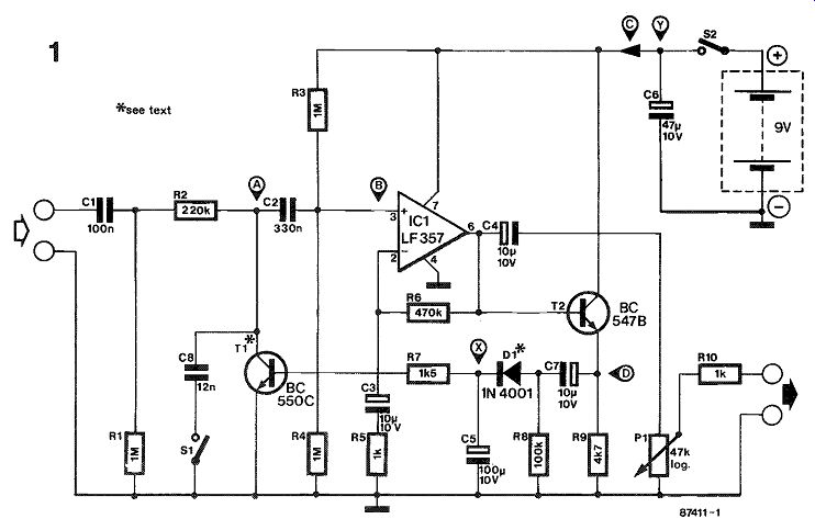
Figure 1 shows the circuit diagram of this compressor. Despite its simplicity, the design responds adequately to a good number of contradicting requirements. As to its dynamic characteristics, an in put signal change from 25 m Vpp to 20 Vpp ( r---s 58 dB) is compressed into an output signal change from 1.5 Vpp to 3.4 Vpp (.4s--7.1 dB). For a less extreme signal change, e.g., from 25 mVpp to 2.5 Vpp (A40 dB), the compressed output signal changes from 1.5 Cpp to 2.25 Vpp (=3.5 dB). The circuit has an extended frequency response from about 7 Hz to 67 kHz nominally, thanks to the use of a fast opamp, the Type LF357 (IC,), which is set up here to provide an amplification of about 471 [(R6 + R5)/R5].
Capacitor C3 blocks the direct voltage at the inverting input of IC1, and with R5 sets the low-frequency roll-off of the opamp alone at about 16 kHz.
Resistors R3 and R4 bias the non-inverting input of the opamp-and hence its output-at half the supply voltage, ensuring optimum linearity. Capacitor C2 feeds the input signal to the opamp while blocking the bias voltage at pin 3. Its value is not critical, but it has some effect on the low-frequency response of the compressor. The attenuator section in this circuit is essentially composed of R2 and the collector of this transistor is held at 0 V with the aid of R1 and R2. In this way, T1 is always operated in its saturation region, and its collector-emitter junction acts as a variable resistance controlled with the current fed to the base. The higher this current, the lower the c-e resistance, and the higher the instantaneous attenuation of the signal fed to IC,. The controlling rectifier is composed of D1-05-R7. Transistor T2 functions to provide the charge current for C7 so as to avoid distortion other-wise incurred by too heavily loading the IC, output.
The rectified voltage across C5 is a direct measure of the output signal amplitude, and forward-biases the base of T,, which regulates the attenuation as discussed. The use of a diode with a low internal resistance, Di, and a buffer, T2, ensures fast charging and slow discharging of C5, and thus a short attack time and a long release time, respectively. As C5 is discharged via R7 and the base resistance of T1, the release time of the compressor is the product of the value of these three components. When the base bias is reduced, the base resistance of T1 increases, lengthening the release time. This is a most welcome feature, especially with speech signals.
The output of the opamp is fed to Ca-Pi- Rio, which provide DC insulation and level adjustment.
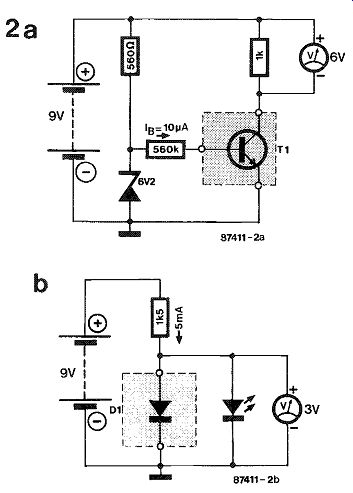
Two compressors are readily combined to make a stereo version by feeding them from a common battery and connecting points X and points Y (never X to Y!). In this case, T1 and D1 in both compressors must be matched types to ensure proper operation. Figure 2 shows two simple test circuits for selecting transistors and diodes with matching DC characteristics. The basic method is to start with noting the voltmeter reading for a particular device, and then find a matching type from an available lot by inserting devices until one is found that gives the preciously noted test voltage. In the diode test circuit, the LED lights to indicate the absence or re verse connection of a diode under test.
A = 0 V B = +4.5 V C = 6 mA D = 3.9 V
All values are typical and within 10%.
All voltages measured with respect to ground with a DMM (Zin = 1 MO).
Provision has been made to use the circuit as a noise suppressor. Referring to Fig. 1, closing S1 connects C8 across the regulator transistor to form a low-pass filter in conjunction with R1 and R2. The cut-off frequency of this LPF is a function of the current sent into the base of Ti. The overall effect thus obtained is an effective elimination of noise from quiet passages in the program. For louder passages, the suppression of noise is not so import ant, as it is then virtually inaudible.
Finally, when using this compressor, make sure that your amplifier has ample cooling provision, because it may well be continuously operated at the top of its power rating. For the same reason, check whether the loudspeakers can handle the available power.
005 CURRENT CORRECTED AF AMPLIFIER
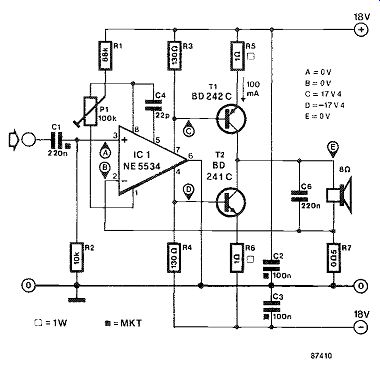
The majority of modern AF power amplifiers drive the loudspeaker(s) with a voltage that is simply a fixed factor greater than the input voltage. It is fairly evident, therefore, that the power delivered by such amplifiers is inversely proportional to the loud speaker impedance, since the cone displacement of a loudspeaker is mainly a function of the current sent through the voice coil, whose impedance may vary considerably over the relevant frequency range. In multiway loudspeaker systems, this difficulty is overcome by appropriate dimensioning of the crossover filter, but a different approach is called for when there is but one loudspeaker.
This amplifier is based on current feedback to en sure that the current sent through the voice coil re mains in accordance with the input signal. The current through the voice coil and R7 develops a voltage across the resistor. A negative feedback loop is created by feeding this reference voltage to the inverting input of IC1. The overall amplification of the circuit depends on the ratio of the loudspeaker's impedance, ZL, to the value of R7. In the present case the amplification is 16 times (ZL/R7 = 8/0.5 = 16).
The connection of the opamp's output to ground is slightly unusual, but enables the base current for output transistors T1-T2 to be drawn from the supply rails, rather than from the opamp. Capacitor C6 functions to set the roll-off frequency at about 90 kHz. The quiescent current of the amplifier is of the order of 50 to 100 mA for class A operation, and is determined by R3-R4 and R5-R6. The complementary power transistors should be closely matched types to avoid fairly large offset currents (and voltages) arising. Some re-dimensioning of either R3 or R4 may be required to achieve the correct balance for the power output stage. The emitter current of T1 and T2 is about 500 mA when the amplifier is fully driven.
The harmonic distortion of this amplifier is less than 0.01% at P0= 6.25 W and Ub = ±18 V.
Source: Texas Instruments Linear Applications.
006 DIGITAL AUDIO SELECTOR
Switching audio signals digitally could be done with the aid of CMOS analog switches or multiplexers.
Simple as this may seem, there is, however, an in evitable loss in the quality of the sound due to the noisy nature of CMOS switches. Furthermore, the high on-resistance of these devices together with the large parasitic capacitances generally present in CMOS circuits causes a high susceptibility to crosstalk. The circuit given here is a novel way of selecting one out of ten audio signals digitally with out any of the foregoing drawbacks.
As shown in the circuit diagram, the ten input signals numbered 1-10 are applied to the bases of transistors T1-T10 via capacitors C1 –C10 respectively. The bias voltages for the transistors are obtained with the aid of R1 –R10. Depending on the binary state applied to IC), one of its outputs Q0 Q9 goes low. For example, if the input code is 0010, Q2 goes low, pulling the base of T3 to 0 V, while the bases of all other transistors are raised to nearly +15 V. Therefore, T3 works as an emitter follower while the other transistors are effectively reverse biased. The output rail of the transistor array is connected to voltage follower IC2, which provides the output signal of the digital audio selector.
Voltage regulator IC3 is required only if a + 5 V rail is not available. If the number of channels required for a particular application is less than 10, the relevant components can be omitted. If a mute facility is required, simply short one input to ground to silence the output on selection of the corresponding channel.
This circuit can handle input signals up to 4 Vrms.
The total distortion does not exceed 0.01% for frequencies up to 20 kHz. The crosstalk incurred in this circuit is less than -80 dB. This value can be attained by paying due attention to the layout of the practical circuit, the decoupling of the supply.
lines (fit C14 and C15 direct to the relevant pins of the opamp), and the use of good quality components.
The measuring values indicated in the circuit diagram were obtained in a prototype. All voltages are measured with respect to ground with the aid of a DMM (Zn = IMO). The channel selected was number 1.

007 DIGITAL VOLUME CONTROL I
This digital potentiometer circuit is a hybrid analog and digital design offering push-button controlled programmable attenuation as well as high to low impedance conversion by means of a single active device. Digital noise is eliminated as effectively as possible through galvanic isolation of digital and analog parts in the input attenuator.
At the heart of the digital control section is a Type 2716 EPROM, which can be Programmed either as shown in Table 1 or to individual requirements, as will be detailed below. At power-on, debouncer bistables N1-N2 and N3-N4 force logic low levels onto EPROM address lines As and A6 respectively, selecting a Programmed address range that supplies the digitally coded, initial volume setting. R-C net work R16-C2 causes gates N7 and Na to generate a clock pulse for IC2, which latches the 8-bit word from IC1, passes this information to driver ICs, and thus determines which relay(s) is/are energized, thereby fixing the attenuation before the AF signal is applied to opamp IC6. Depression of S (up) or S2 (down) causes the corresponding address line As or A6 to go low, selecting a certain address range in the EPROM. The exact address location is determined by the value last latched into IC2 after either key has been released. It is readily seen that the five available data bits at the Q1 Qs outputs of IC2 allow 32 (25) simulated potentiometer set tings.
Table 1

The digital control section has been designed to offer an auto-repeat function when either one of the step control keys is kept depressed; oscillator gate N6 then provides a clock pulse train to N7-No, and so causes successive addresses in IC1 to be scanned automatically, until either the lowest or highest possible volume setting is reached, at which moment the circuit forces itself to a hold state, which can also be selected at any time by simultaneously depressing the up and down key.
S3 enables the user to select a further address block, Programmed with another set of volume steps; the circuit as shown, along with the data from Table 1 arranges for 3 dB steps.
The analog section of the circuit is basically a four-section, relay-controlled attenuator composed of resistor networks to achieve a signal attenuation in 3 dB increments, as defined with the relevant bit pattern at the Q1. .Q5 outputs of IC2. Rea (Q5), if deactivated, enables IC6 to amplify its input signal by 3 dB. The inset resistor and preset combination may be used take over the function of C10, since the latter should be a high stability foil type, which may be a rather difficult to obtain part. Both circuit alternatives function as click suppressors when step ping through the available range of volume settings.
The preset, if used, should be set for zero offset voltage at pin 6 of the opamp; replace Cm with a wire link.
It is suggested to use miniature DIL relay types in the Re1 Res positions, while all resistors in the attenuator are preferably close tolerance (1%), high stability types. Also observe that the supply voltages to analog and digital section are kept well apart and decoupled so as to preclude introducing switching pulses and digital interference in the sensitive attenuator sections as well as the opamp output stage.
Finally, Table 1 offers a suggestion for programming the EPROM with data to achieve circuit operation as set out above.


008 DIGITAL VOLUME CONTROL II
Many of today's hi-fi amplifiers feature a "clicking" volume control, but this is only rarely a real stepped attenuator based on a wafer switch. In nearly all cases, this expensive system is based on a normal potentiometer, whose spindle is fitted with a mechanical construction to simulate the stepping movement. A normal rotary switch is not suitable for adjusting the volume of an amplifier because it briefly disconnects the input from the signal source when operated, and so readily gives rise to clicks and con tact noise.
Different problems crop up when designing an electronic volume control. Of these, distortion is probably the hardest to master, but reasonable results are still obtainable, as will be shown here.
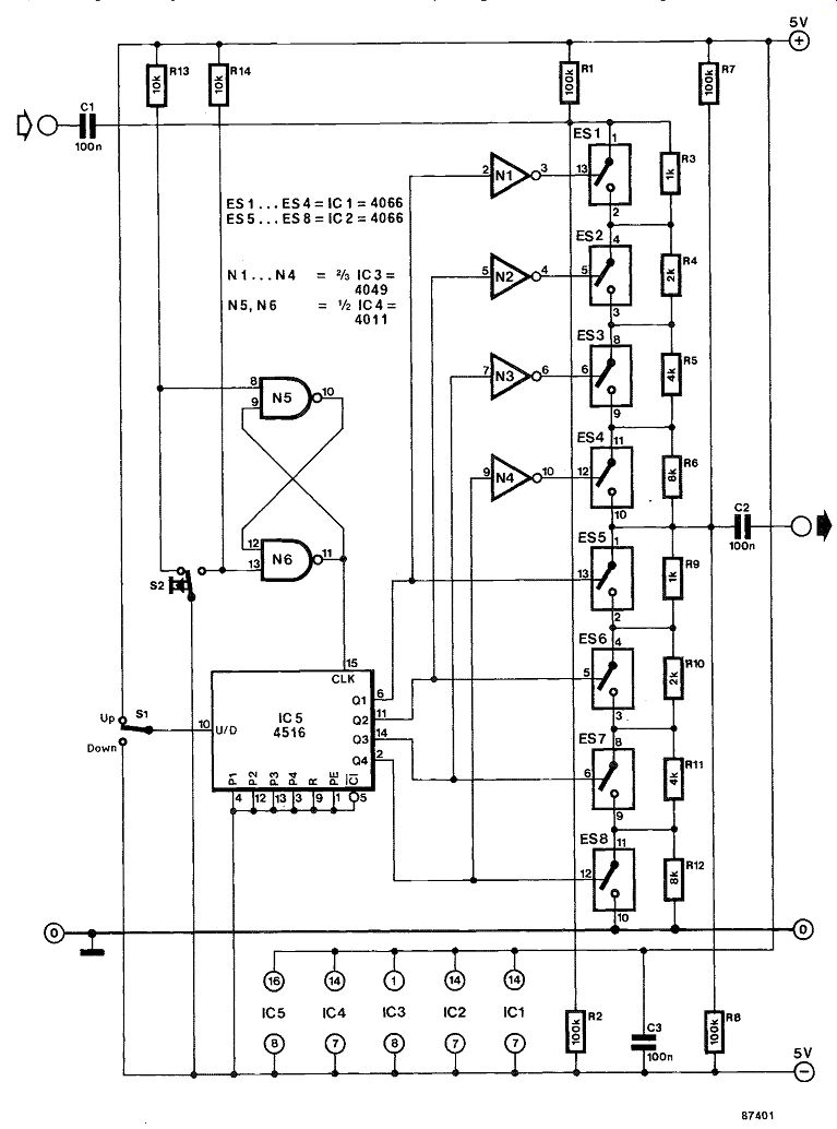
Basically, there are two methods for making an electronic potentiometer. One is to create a tapped resistor ladder (which is not much different from a normal potentiometer), the other is to change the resistance of the two "track sections" such that the total resistance remains constant. The circuit pro posed here is based on the second method, and features 16 steps in its basic form. The number of steps can be increased to, say, 64 by adding four switches and resistors.
The electronic potentiometer is composed of two equal sections, which have a total resistance of 15 k-Ohm each. The electronic switches in each section are controlled by binary counter 105. Since the switches in section ESI-ES4 and those in ES5-ES8 are controlled in complementary fashion, the total resistance of the potentiometer remains constant.
Resistors R1-R2 and R7-R8 serve to keep the potential at the input and output at 0 V so as to preclude clicks when the step switch, S2, is operated. Switch S1 is the up/down selector. Gates N5-N6 form a bistable to ensure that the counter is clocked with debounced step pulses.
The number of steps can be increased by adding a counter and the required number of electronic switches, divided over the two "track sections".
These switches are then connected in parallel with resistors whose values correspond to binary order 1 2-4-8, etc., as shown in the circuit diagram. Fortunately, precise binary ratios are not required here, since adequate results are obtainable with approximations of the theoretical resistance values, and as long as the actual resistors are kept equal in both sections.
---------------
009 DISCOMIXER
This mixer is a typical example of the way modern components can, and do, simplify the realization of good quality audio circuits. In the given configuration it is eminently suitable for use as a disco-mixer, but the number of input channels can easily be enlarged.
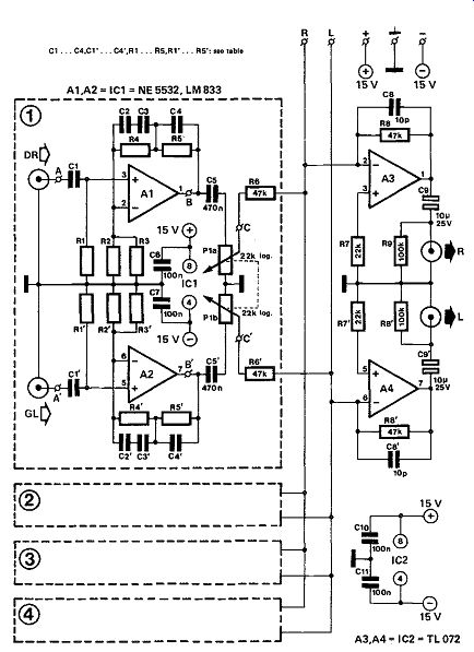
As can be seen in figure 1, in its basic form the mixer has four input channels. These could, for in stance, serve as inputs for a microphone, stereo pick up, and cassette player or tape recorder.
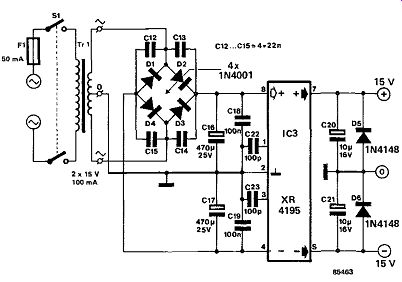
The power supply has been kept as simple as possible; if it proves difficult to obtain the XR4195 regulator IC, it may be replaced by a combination of a 78L15 and 79L15. The transformer is preferably of the PCB type to keep the mixer as compact as possible.
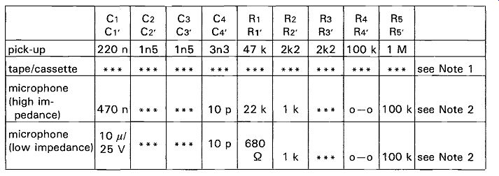
The values of C1 and R1 are dependent on the type of microphone used. If this is a high-impedance type, the values should be 470 nF and 22 k-O respectively, whereas with low-impedance types, 10 µF and 680 ohm are required.
Unfortunately, miniature bipolar electrolytic capacitors (C1, C1', C9, and C) are not yet available everywhere, although they are almost indispensable in applications such as described here.
Standard electrolytics may be used with maximum reverse voltages of 1 V, but their use introduces distortion and premature ageing (because of the re verse polarity).
-----------
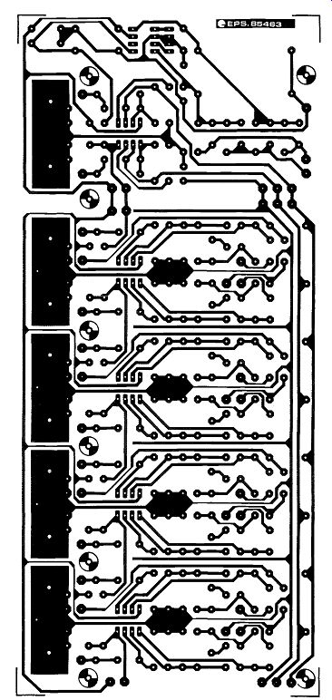
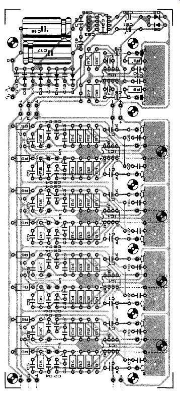
Provision has been made on the printed circuit board for up to four channels. Two or more PCBs may be connected together; the output and supply sections may then be cut off as required.
Current consumption is about 10 mA per channel.
Parts list:
Resistors:
R.1*...Rs*,Rv*...R5'* see table
Rs*,Rs*,Ra, Ra' = 47 k R7,RT = 22 k R9*,Rw* = 100 k Pia*,Pib* = 22 k stereo slide potentiometer, log, 58 mm long
Capacitors:
= see table
Cs*,Cs' = 470 n
Cs",C7",C1o,C11,C1a,C1s = 100 n
Cs,Ca' = 10 p
Cs,Cs' = 10 /1/25 V
C12,C13,C14,C15 = 22 n
C1e,C17 = 470 p/25 V
C2o,C21 = 10 p/16 V
C22,C23 = 100 p
Semiconductors:
D1 . . .D4 = 1N4001
D5,D6 = 1N4148
IC1* = NE5532 or LM833
IC2 = TL072
IC3 = XR4195
Miscellaneous:
Tr1 = mains transformer, secondary 2 x 15V/100 mA
F1 = fuse, 50 mA, delayed action
S1 = DPST on/off switch
Single-hole fixing chassis phono socket- 2 per channel
PCB 85463
*One of each required per channel.
--------- Table 1.
Note 1. Wire links A-B and A'-B' required; IC1, C6, and C7 not required.
Note 2. With mono microphones, use input R; do not connect Pi b; wire link C-C' required; all accented components not required.
o-o = wire link
*** = not required
-----
-----
010 HEADPHONE AMPLIFIER
OP-50 Power operational amplifier Features:
Open-loop gain:
Input offset voltage:
Input bias current:
Offset voltage drift:
Common mode rejection ratio:
Power supply rejection ratio:
Noise level:
V/V min.
25 IN max.
5 nA max.
0.3 NV/°C max.
126 dB min.
126 dB min.
5.5 nV//Hz (f=10 kHz) 4,5 nV/V-Hz (f =1 kHz)
Output current: ± 50 mA
Drives capacitive loads up to 10 nF.
On-chip thermal shutdown circuit.
Data taken from manufacturer's data sheet.
There is little doubt that the headphone amplifier described here belongs in the so-called high end class of audio equipment, and is, therefore, perfect for incorporation in, or adding to, the Top-of-the-range Preamplifier described in (ii, although it is also suitable as an autonomous, high quality, unit.
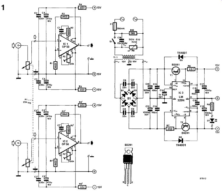
The circuit diagram of the headphone amplifier appears in Fig. 1. The unit is based on Type OP-50 power operational amplifiers, whose technical features are summarized in Table 1. Clearly, everything feasible has been done by the manufacturers, Precision Monolithics Inc., to ensure optimum operation of the device, and it is with this in mind that the remainder of the amplifier was de signed.
------------
Both supply rails to the amplifier ICs are adequately decoupled and filtered with a small series resistor, (R4-R5) and a combination of an electrolytic and a solid capacitor (C4-C2 and C5-C3). With reference to the upper of the two identical channels, preset P2 enables compensating the (small) offset voltage at the output of the OP-50, while Cl-R3 forms a compensation circuit to minimize overshoot for a given closed-loop voltage amplification, AVCL. In the present application, AVCL is about 6, since Rt -=R2/(Avu-1) When it is intended to alter the amplification, R2 should be left at 20 kg. Also observe that the indicated values for R3 and C, are valid when AVCL is between 5 and 20, while R3 = 3.3 kg and C, =1 nF when AVCL is between 20 and 50. No R-C compensation is required when Am. is greater than 50.
The +15 V supply for the headphone amplifier is a relatively extensive circuit based on a precision regulator Type LM325, which features excellent noise suppression whilst ensuring smooth and simultaneously rising output voltages at power-on. Mains-borne interference and clicks from S, are suppressed in varistor R9 and high-voltage capacitor C19. The four diodes in rectifier bridge B, are bypassed with rattle suppression capacitors to en sure minimum noise on the supply rails to the opamps.
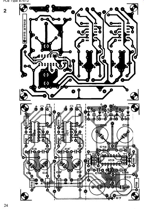
The headphone amplifier can function optimally only if great care is taken both in the choice of the components and in the construction on PCB Type 87512, details of which are shown in Fig. 2. As already stated, the headphone amplifier is suitable for building into the Top-of-the--Range Preamplifier.
This makes it possible to feed the ± 15 V regulator from the raw voltage across C9 (+) and C, 0 I-) of the existing ± 18.5 V supply, while the inputs of the volume control of the headphone amplifier are driven direct from the outputs of IC4 (R) and IC4' (L).
Opamps IC, and IC2 should be soldered direct onto the PCB, and are preferably fitted with a DIL-type heatsink. Provision has been made to screen the amplifiers and the supply on the board by means of two sheets of brass or tin plate, which are mounted vertically onto the dotted lines, and secured with three soldering pins each. Series regulators T, and T2 can do without a heat-sink. When the board is complete, its underside should be thoroughly cleaned with a brush dipped into white spirit or alcohol to remove any residual resin. Next, the track side is sealed with a suitable plastic spray.
When possible, use insulated sockets for the stereo input and output of the amplifier. At the input side, few problems are expected to arise when using gold plated phono sockets mounted onto a separate ABS or epoxy plate. When a good quality, insulated, 6.3 mm, stereo headphone socket proves unobtainable, the nearest alternative is a non-insulated type, whose common tag is connected direct to the ground point on the PCB, between C17 and C18 to effect central earthing. Mains transformer Tr1 is preferably a toroidal type fitted behind a metal screen to ensure minimum hum and other interference picked up by the amplifier inputs. Presets P2 and P2' are trimmed for minimum offset voltage at the respective amplifier output-this is likely to re quire a very sensitive DMM. The headphone amplifier can be terminated in 100 ohm to 1 kg, and is therefore perfect for use as a high-quality line driver also. The outputs are short-circuit resistant.
Finally, a brief summary of the amplifier's expected performance at Vo = 6 VMS and AvcL 6:
Total harmonic distortion: 0.0025% (100 Hz);
0.003% (1 kHz); 0.011% (10 kHz).
Signal-to-noise ratio: ..80 dB.
Response flatness: ± 0.4 dB from 10 Hz to 20 kHz.
Literature references:
(1) Top-of-the-Range Preamplifier. Elektor Electronics, November and December 1986, January 1987.
(2) Linear and Conversion Applications Handbook (1986). Precision Monolithics Incorporated.
Parts list Resistors (± 5%):
F11;R1=4K02F*
R2; R2' = 20KOF
R5; Rs' = 560R R4;R4';R5;R5';R6;R7=2R2 R8 = 820R; 0.5 W
Re= SIOV S10 K250 varistor (Siemens; Electro Value (0784) 33603).
R10=2M2
P1 = 25K logarithmic stereo potentiometer.
P2; P2' = 100K multiturn preset.
Capacitors:
C1;C1=4n7
C2;C2';C3;C3' = 220n
C4;C4';C5;C5'=4701.,z; 16 V; radial
C6;C7;C8;Co=22n
C10;C12=1000 ; 25 V; radial
C11;C13;C15;C16=100n
C14=11.4; 16 V; tantalum
C19 = 22n; 250 VAC
Semiconductors:
... D6 incl.= 1N4001
D7 = LED red
IC1;IC2=0P-50 (Precision Monolithics Inc.)
IC3=LM325 T1;T2=BD241
Miscellaneous:
F1 = 250 mA delayed action fuse plus panel-mount holder.
Tr1= 2 x 15 V; 15 VA 2 x 0.50 A) toroidal mains transformer, e.g.
ILP
Type 03013.
DIL-14 heat-sink for IC, and IC2.
Mains entrance socket.
PCB Type 87512 = SPST miniature mains switch.
Stereo 6.3 mm headphone socket, preferably insulated.
2 off phone input sockets.
Suitable metal enclosure.
* See text
--------------
011 HI-FI HEADPHONE AMPLIFIER
This 1-watt amplifier lends itself par excellence for use as driver for a low impedance headphone or as output stage in a hi-fi preamplifier driving an active loudspeaker. Many preamplifiers do not permit long, unscreened leads to be connected to them, but the present amplifier accepts these happily.
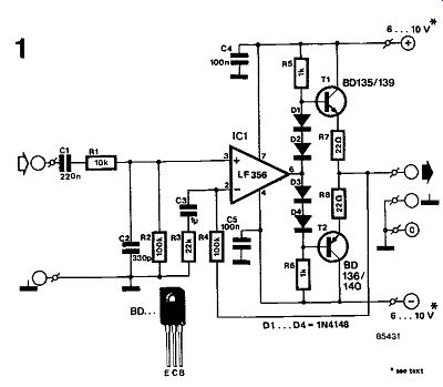
The circuit--figure 1--consists of an opamp type LF 356 and a push-pull transistor output stage.
Low-pass filter R1/C2 at the input limits the slew rate of the input signal. In conjunction with the relatively fast LF 356, this results in very low delay distortion. The fixed quiescent current of 30 mA drawn by the output transistors, and set by diodes D1 ... D4 in conjunction with emitter resistors R7 and R8, ensures very low crossover distortion.
Feedback resistors R3 and R4 fix the gain at about 15 dB. The consequent overall distortion with a -3 dB bandwidth from 10 Hz to 30 kHz is only 0.1 percent.
The amplifier delivers a maximum power of 1 watt into 8 ohm for an input signal of about 500 mVrms.
High-impedance headphones and 4 ohm loudspeakers may also be connected without detriment.
The amplifier is best built on the printed circuit board shown in figure 2. To enable it surviving a short circuit at the output, the two transistors should be mounted on heat sinks - do not forget the insulating washers and the heat conducting paste! The power supply need not be more than a simple affair, consisting of a mains transformer with a center-tapped, 6 . . .8 V, 0.5 A secondary, a suitable bridge rectifier, and two 1000 uF/16 V electrolytic capacitors in a conventional arrangement.
To drive high-impedance headphones at high volume, you need a ± 15 V regulated power supply:
in some cases, this may be derived from the pre amplifier supply. In this arrangement, care must be taken not to short-circuit the output terminals.
Parts list
Resistors:
R1 = 10 k
R2, R4 = 100 k
R3 = 22 k
R5, R6 = 1 k
R7, R8 = 22 ohm
Capacitors:
C1 = 22 n
C2 = 330 p
C3 = 1 u
C4, C5 = 100 n
D1 ... D4 = 1N4148
T1 = BD 135 or BD 139
T2 = BD 136 or BD 140
IC, = LF 356
Miscellaneous:
PCB 85431
Heat sinks for T1 and T2
-------

-------
012 HIGH DYNAMIC RANGE MIXER
A mixer is expected to have low-noise and high dynamic performance. Most standard mixers use inverting operational amplifiers. Unfortunately, the noise figure of many opamps is poor, and opamps with a good noise figure are normally not suitable for operating with large signals.
The noise factor of standard circuits is often made even poorer because the source and amplifier are not properly matched.
The characteristics of a mixer can be greatly improved, therefore, by the use of buffers at the input stages, and the constructing of operational amplifiers from good-quality transistors. This has been done in the accompanying circuit. The input is buffered by T1 and T2. The input impedance of T1 can be ignored, so that the source merely needs to be matched with Pt The opamp is formed by transistors T3 to T8 incl.
Good-quality RF transistors have been used in differential amplifier T3-T4-T5. These transistors have a better noise figure at a greater bandwidth than AF types.
The proposed circuit has a frequency range (-3 dB points) of 10 Hz to 80 kHz; third harmonic distortion of not more than 0.05 percent at 10 kHz and an output voltage of 9 Vpp; and a signal-to-noise ratio of 100 dB.
The signal-to-noise ratio applies to an output signal of 9 Vpp with open-circuit input, and a bandwidth of 20 kHz. The maximum value of the output signal is about 12 Vpp, measured across a load impedance of 560 ohms. If the mixer is terminated by a higher impedance, the output voltage will be greater.
A further advantage of the circuit is that the popular valve sound may be realized in a simple manner. To this end it is necessary that T1 and T2 commence limiting at a slightly lower level, i.e. 12 Vpp input, than the composite opamp. The supply voltage of T1 and T2 must then lie between ± 6 V and ± 9 V. Since T2 is connected as a current source, the exact supply voltage can be set with the 2k2 preset at the wanted clipping level.
If desired, the output off-set may be zeroed by inserting a 50 kilo-ohm preset in the base circuit of T4.
This base should also be decoupled by a 1µF, 63 V capacitor.
The current consumption of the opamp is about 35 mA and that of the buffer stages not more than 10 mA. If, therefore, ten buffer stages are used, the power supply should be capable of providing 150 mA at ±15 V.

----------
013 INTEGRATED STEREO AMPLIFIER
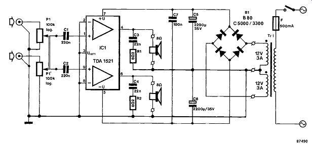
The Type TDA1521 from Valvo/Mullard is an integrated HiFi stereo power amplifier designed for mains fed applications such as stereo TV. The device works optimally when fed from a ± 16 V supply, and delivers a maximum output power of 2 x 12 W into 8 ohm. The gain of the amplifiers is fixed internally at 30 dB with a spread of 0.2 dB to ensure optimum gain balance between the channels.
A special feature of the chip is its built-in mute circuit, which disconnects the non-inverting inputs when the supply voltage is less than ± 6 V, a level at which the amplifiers are still correctly biased.
This arrangement ensures the absence of unwanted clicks and other noise when the amplifier is switched on or off. The TDA1521 is protected against output short circuits and thermal overloading. The SIL9 package should be bolted onto a heatsink with a thermal resistance of no more than 3.3 K/W (RL= 852; Vs= ± 16 V; Pa =14.6 W; To = 65 °C). Note that the metal tab on the chip package is internally connected to pin 5.
The accompanying photograph shows that this high quality stereo amplifier has a very low component count, and is readily constructed on a piece of Veroboard.
The following technical data are stated as typical in the datasheets for the TDA1521 (RL= 8 ohm; Vs = ± 16 V):
Distortion at Po =12 W:
Quiescent current:
Gain balance:
Supply ripple rejection:
Channel separation:
Output offset voltage:
3 dB power bandwidth: 0.5% 40 mA
0.2 dB 60 dB 70 dB 20 mV
20-20,000 Hz
------------
014 LOUDSPEAKER PROTECTION I
There are many ways of protecting loudspeakers against the switch-on 'plop': many of these rely on a clamp circuit across the power amplifier input to hold this at 0 V for a few seconds after switch-on.
Others, like the one suggested here, depend on a relay to switch off the loudspeaker(s).
----------
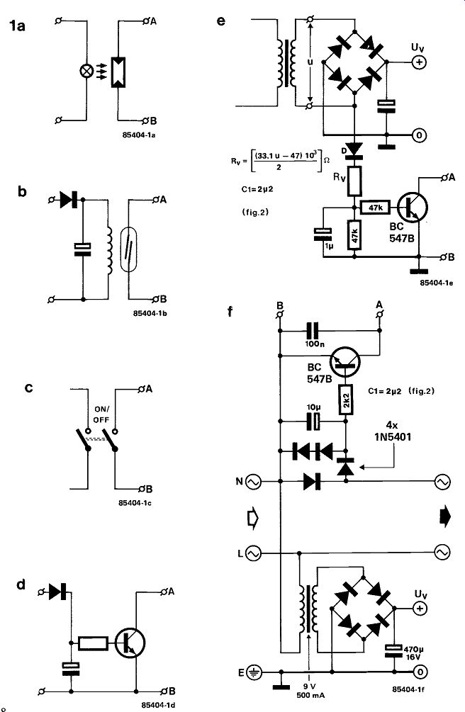
Terminals A and B of the circuit in figure 2 are connected to one of the sensing circuits in figures 1a . . .1f, of which the pros and cons will be discussed shortly. Whichever of these circuits is used, A is shorted to B immediately the power is switched on. This cuts off transistor TI instantly, which causes capacitor C1 to charge. After a few seconds, the voltage across C1 causes zener D2 to break down. Transistor T2 and T3 then conduct; the relay is energized, and the loudspeakers are connected in circuit.
When the power is switched off, T1 conducts and this causes C1 to discharge very rapidly. The voltage across C1 quickly drops below the breakdown level of D2; transistors T2 and T3 are cut off, and the relay returns to its quiescent state, which disconnects the loudspeakers.
Input circuit la relies on a light-dependent resistor (LDR) fitted close to the mains on indicator lamp.
When the lamp lights, the resistance of the LDR drops sharply, so that terminal A is virtually shorted to B.
The input in lb relies on a reed relay connected to the secondary winding of the mains transformer. As soon as the mains is switched on, the relay contacts close.
The third possibility, shown in Ic, is that the mains on/off switch has a third contact that connects A to B when the mains is switched on.
A further option is illustrated in 1d, where a transistor is connected to the secondary of the mains transformer via a diode and resistor. The transistor conducts when the mains is switched on.
The inputs in le and if also provide power for the protection circuit. That in le has a bridge rectifier connected across the secondary winding of the mains transformer. When the mains is switched on, the BC 547 conducts and shorts A to B.
Finally, the circuit in If is connected direct to the mains. Here again, as soon as the mains is switched on, the BC 547 conducts and terminal A is shorted to B.

-----------
Whichever of the input circuits is used depends on circumstances and/or individual preferences. If one of circuits 1a . . . 1d is used, a separate power supply is required for the protection circuit. As suggested, the output voltage, Uv, of this should be 40...60 V d.c. For lower values of Uv, the rating of D2 must be reduced accordingly.
Resistance R1 depends on the relay used, and is calculated from
= [(Uv - Ur - 2.5)//,] where U, and Jr are the operating voltage (in volts) and current (in amperes) of the relay used respectively.
The relay contacts must be able to carry a large current: 10 A is not unusual in many amplifiers.
The rating of Rv is [U,/,] W.
If the 'plop' is still heard, increase the value of R3 as required- in reasonably small steps.
015 LOUDSPEAKER PROTECTION II
This is an all-transistor design for incorporation in AF amplifiers that produce nasty clicks in the loud speakers when turned on or off, jeopardizing the voice coils by passing a large current surge.
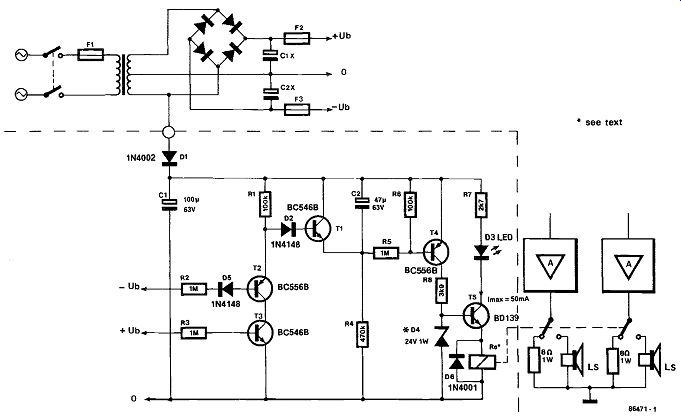
Assuming that AF amplifier and protection circuit are off, C1 and C2 are empty of charge and Re is deactivated. At power-on, D1 rapidly charges C1.
Provided both the negative and the positive supply voltage are present and at the correct level, T2 and T3 conduct, while T1 is off, enabling C2 to be slowly charged via R4. If the voltage across C2 is sufficiently high for T4 to conduct, T5 will draw base current and energize Re, which connects the loudspeakers to the amplifier outputs. Zener diode D4 fixes the voltage across the coil of Re, so that differently rated relays may also be used in the circuit, provided D4 is changed accordingly. However the relay coil current should not exceed about 50 mA, while the changeover contacts should be rated in accordance with the amplifier output power and impedance; for a 2 x 100 W at 8 ohm type, for in stance, the relay contacts should be rated at least 8 A.
Should either one or both supply voltages (-Ub; + Us) disappear for some reason or other (amplifier malfunction, short-circuited smoothing capacitor, etc.), the relevant transistor T2 or T3 will be disabled, causing T1 to receive base current via R1; C2 will be discharged forthwith and Re is deactivated in consequence since T4 and T5 are turned off. The amplifier channels can now produce clicks they like; the output is safely applied to two resistors matching the output impedance.
The protection circuit is fed off the voltage across C1, which is purposely rated at only 10014F to enable Re to be deactivated almost immediately after the amplifier has been switched off. Power-off clicks, if produced, will therefore end up in the dummy resistors rather than the expensive loudspeaker voice coils.
The protection unit is most readily fitted on a piece of veroboard, while Re should be mounted close to the loudspeaker output terminals to keep contact losses as low as possible.
------------
016 LOUDSPEAKER PROTECTION III
Many modern AF power output stages are capable of delivering considerable power levels in the super sonic frequency range. When the loudspeaker cannot handle that power, the voice coil is rapidly overheated, and causes a short-circuit. If the power output stage is not properly protected, it breaks down and supplies a direct current that effectively destroys the loudspeaker.
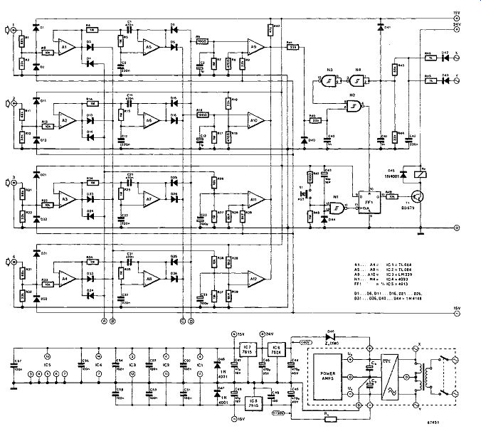
The present loudspeaker protector is composed of three sections: a measuring amplifier, a detector, and a relay driver. Four channels are shown here as an example. Potential divider R1-R2 determines the sensitivity of the protection circuit, while D1-D2 protect the input of Al. Opamp A5 is set up as a low pass filter with a cut-off frequency of 0.5 Hz, so that it can function as a DC detector. The second section of the circuit is composed of four detectors A5 – A12. As compares any negative direct voltages to a reference set with Rs-Rs, while C3-R7 determine the delay time. Opamp A 10 has a similar function for positive direct voltages. The circuit is actuated when VisR2 0.65 > 15R2 It + R2 128+119
Comparators All and Al2 function as the power limiter. Positive and negative peak voltages are rectified in D3-D4 and averaged with the aid of R-C combinations R36-C33 and R26-C23 . The relatively long periods of these networks precludes erroneous triggering of the circuit on peaks in the input signal.
The power limiter is actuated when VinR2f2 15R28
0.65 > R1 + R2 R28 + R29
This equation is also valid for the positive detector set up around Al2. The stated component values result in Pmax"='30 W in 8 ohm.
When the input signals are all right, the open collector outputs of As- Al2 are in their high impedance state, so that the output voltage is + 15 V via R40. When a fault condition exists at one or more of the inputs, junction R40-R41 is pulled down to -15 V.
The central part in the relay driver is bistable Gate Ni is a resettable power-up delay circuit which clocks FF, . The logic high level at the D (data) in put is only transferred to output ohm when the R (reset) input is logic high. It is seen that a reset pulse can originate either from the mains detector N3-N4, or from the fault detectors As-Al2.
The loudspeaker protector is conveniently fed from the amplifier's symmetrical supply, but care should be taken to dimension D48 and such that the indicated voltage across C44 and C45 is not exceeded.
If the amplifier supply delivers less than 28 V, IC6 may be omitted, and the loudspeaker relay, Re, re placed with a 12 V type fed from the + 15 V rail.
Voltage divider R43-R44 should then be re-dimensioned such that the input of N4 is held at about +13 V when R43+ k-Ohm.
--------------
017 LOW NOISE RIAA PREAMPLIFIER
This high quality phono preamplifier is based on the Type HA12017 integrated circuit from Hitachi.
The principal technical data of this chip are summarized in Table 1. The circuit diagram, Fig. 1, shows that output offset correction is provided by integrator IC2. The output signal of IC is first passed through low-pass filter R7-C9, then integrated in IC2-C8. The error signal is fed to the inverting input of amplifier IC1 via 47 162 resistor R6. The amplitude of this signal is always such that the offset voltage at the output of IC1 is virtually zero. The offset correction used here enables the preamplifier to drive a power amplifier direct.
The correct capacitive termination of the pick-up cartridge can be selected with the aid of S1. The input impedance is 50 k ohm, but can be altered by re-dimensioning R2-R3. The output impedance of the preamplifier is 510 ohm, i.e., low enough for driving a relatively long cable.
The RIAA equalization filter in the negative feed back circuit of IC1 is fairly complex, which was necessary to meet the required IEC specification (note the use of high stability capacitors and resistors).

-----------
Table 1. HA12017 Low noise preamplifier
Features:
IN Low noise: Vn [in] = 0.185 µV typ. (measured in IHF-A network, Rg = 43 k-Ohm, IEC RIAA). V0=-95 dB relative to Vo=1 Vrms.
MI Wide dynamic range: V:=235 mVrms max. (Vco= ± 24 V, f =1 kHz, THD=0.1%, Ao----100A40 dB).
Low distortion: THD =0.002% typ. If =20-20 000 Hz, Vo=10 Vrms, RIAA equalization).
MI Supply ripple rejection: SVRI +Vco)=56 dB; SVRI-Vcc) = 45 dB (typical values at f = 100 Hz and Rg = 43 K2).
Maximum operating voltage: ± 26 V.
Maximum power dissipation: 500 mW at Ta =75°C.
Note: Rg =114. in this design.
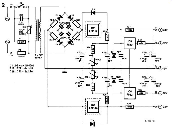
The regulated power supply for the phono preamplifier is shown in Fig. 2. This is once again a relatively extensive circuit which, in combination with the low-pass filters on the ± 24 V lines to IC1 and IC2, gives excellent suppression of RF signals, hum, rectification noise, and mains borne interference. Presets P1 and P2 serve to adjust the output voltage on the ± 24 V rails.
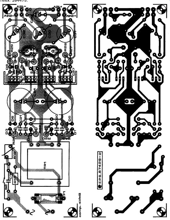
The printed-circuit boards for the preamplifier and the power supply are shown in Figs. 3 and 4 respectively. The correct values for R 1, C4 and C5 are achieved by parallel and series connection. All four voltage regulators can be fitted onto a common heatsink if electrical insulation is provided. The ac companying photograph shows a suggested construction of the preamplifier.
It is strongly recommended to use good quality components for the volume adjustment and input source selection--consult the references given below.
References:
1. Top of the range preamplifier, Elektor Electronics, January 1987.
2. Valve preamplifier, Elektor Electronics, March 1987.
3. Electronics potentiometers, Elektor Electronics, April 1987.
Parts list:
Resistors (±5%):
R1 =240R R2;R3=100K R4=43K R5=51OR Rs=47K R7;R8 = 1 M-O
Rs=1K6 Rio= 165RF R1 1 = 3K1 6F + 4K 64F Ri2= 95K3F R13. .
.R16 inCi.;R27...R30 incl.=1OR R17=2M2 R18= varistor S10V S10K250 (Siemens) R . . R22 incl. = 1R8 R23=22OR R24=3K9 R25= 120R R26=2K0 Pi;P2=250R preset
Capacitors:
C1 =10t2; MKT
C2= dimension to suit capacitive termination of cartridge.
C3= 100p; polystyrene
C4=2n7F//6n8F//150p0F; styroflex
C5=1n0F//33n0F; styroflex
C6= 100p styroflex
C7 = 470p styroflex
Cs;Cs=470n MKT
C10;C12.;C14;C1s=220n MKT
C11;C13;C25;C30=1000 ohm; 25 V; radial
C15;C17=100µ; 25 V; radial
C16=22n; 630 V
C19 ...C22 incl.=22n
C23; C24=47001.4; 40 V; radial
C25; C26= 1µ; 40 V; radial
C27;C28= 100n
C31;C32=2200µ; 40 V; radial
Semiconductors:
D1 ...D8 incl.=1N4001
IC1 = HA12017 ( Hitachi)
IC2=0P-77 (Precision Monolithics Inc.)
IC3=LM317
IC4=LM337
IC5=7812
IC6= 7912

-----------
Miscellaneous:
S1 = 4-way DIP switch block.
S2 = SPST mains switch.
F1= 250 mA delayed action fuse with PCB mount holder.
T R1 = 2x24 V;100 mA mains transformer for PCB mounting.
Heat-sink for IC3. . ICs incl.
Insulating washers for IC3. ..IC6 incl.
PCB Type 87429-1 and 87429-2
Available from Electro-Value Ltd MI 28 St Judes Road Englefield Green Egham Surrey TW20 OHB. Telephone: (0784) 33603 IIII Telex: 264475.
Available from Cirkit PLC III Park Lane Broxbourne Hertfordshire EN10 7NQ.
Telephone: (09921 444111 III Telex: 22478.
Stock number: 61-170-12017.
General note: many special AF components for this project are available from Audiokits Precision Components 6 Mill Close Borrowash Derby DE7 3GU. Telephone:
103321 674929.
----------------
018 MICROPHONE AMPLIFIER WITH MUTE SWITCH
Microphones, unfortunately, produce only a small signal and they, therefore, require a special pre amplifier to boost their output. Because small signals are involved, the signal-to-noise ratio of the preamplifier is a very important parameter.
In this article, we present two circuits for a pre-amplifier suitable for virtually all occasions: a sym metrical and an asymmetrical version. We have incorporated a mute switch, which speakers can use when they want to clear their throat. As there is an number of low-noise operational amplifiers available nowadays, the cost of these pre-amplifiers is relatively low.
The asymmetrical version is shown in figure 1.
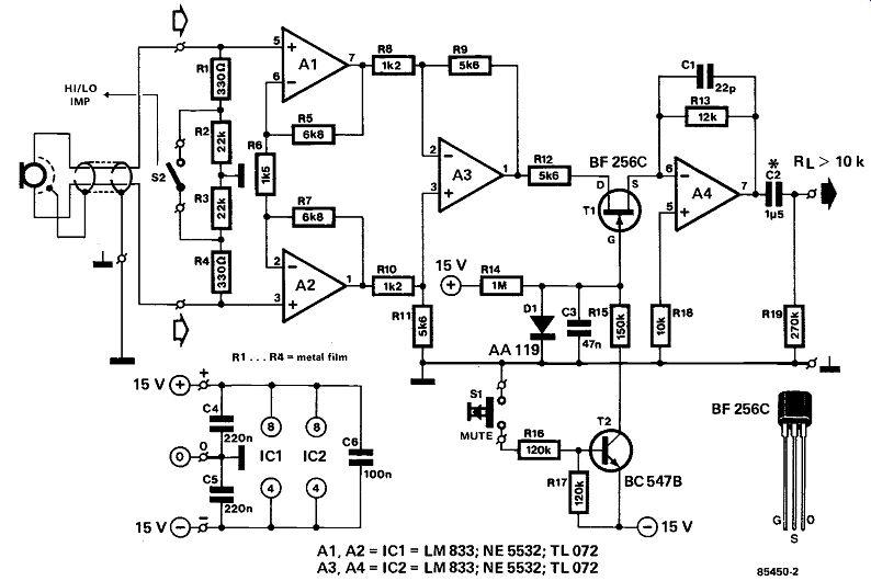
Switching between high and low impedance matching is possible with switch S2. Opamp A1 is arranged as an AC amplifier with a gain of around 27 dB. This stage may also be used as a DC amplifier: R3 and C1 are then omitted, and the value of R2 is lowered to 22 k. Capacitor C2 limits the band width of the amplifier to ensure stable operation.
Irrespective of whether A1 functions as a DC or an AC amplifier, the DC component in its output is blocked by C3. The amplified AC signal is applied to muting stage T1. This field-effect transistor (FET) normally conducts and the output of A1 is then further amplified in A2 by about 5. Finally, the signal is taken to the output terminal via high-pass filter R13-C6. The load must be greater than 10 k-O.
When mute switch S1 is pressed, the FET receives a negative voltage at its gate and is switched off. Capacitor C5 determines the speed with which muting occurs within certain limits. Capacitors CI, C3, and C6 may be electrolytic types: measure the DC level at both terminals to determine which way they should be connected!
Figure 1. Circuit of the pre-amplifier with asymmetrical input.

------------- The symmetrical version of the pre-amplifier is shown in figure 2. The only difference between this and that in figure 1 is that the input stage now consists of A1, A2, and A3 to obtain symmetry. Opamps A1 and A2 provide a total gain of about 20 dB.
Opamp A3 functions as a differential amplifier to ensure that common-mode noise and interference is effectively suppressed.


---------
Figure 2. Circuit of the pre-amplifier with symmetrical input.
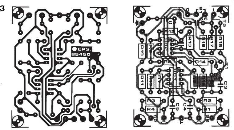
Figure 3. Printed circuit board for the asymmetrical pre-amplifier.
Figure 4. Printed circuit board for the symmetrical pre-amplifier.
Parts list (figure 3)
Resistors:
R1= 680 O metal film
R2,R3 = 47 k metal film
R4,R7,R12 = 22 k
R5 = 1 k
R6 = 4k7
R8 = 1 M
Re = 150 k
R10, R11 = 120 k
R13 = 270 k
Resistors:
R1, R4 = 330 ohm metal film
R2,R3 = 22 k metal film
R5,R7 = 6k8
R6 = 1k5 R8, R311) = 1k2
R9, R11, R12 = 5k6
R13 = 12 k
R14 = 1M
R15 = 150 k
R16,R17 = 120 k
R18 = 10 k
R19 = 270 k
Capacitors:
Capacitors:
C1 = 1 p/16 V MKT (see text) C1 = 22 p C2 = 22 p C2 = 1p5 MKT (see text) C3 = 2p2 MKT (see text) C3 = 47 n C4 = 10 p C4,C5 = 220 n C5 = 47 n C6 = 100 n C6 = 1p5 MKT (see text) C7,C8 = 220 n
Semiconductors:
Semiconductors:
= AA119
= BF256C T2 = BC547B IC1 = LM883; NE5532; TL072
Miscellaneous:
S1 = spring-loaded push to make switch
S2 = miniature SPST switch PCB 85450-2
= AA119
= BF256C T2 = BC5476 IC1,IC2 = LM833; NE5532; TL072
Miscellaneous:
= spring-loaded push to make switch
S2 = miniature
SPST switch PCB 85450-1 PCB 85450-2
MKT = metal-plated plastic polythereftalate foil
019 MICROPHONE-SIGNAL PROCESSOR
In broadcasting systems, intercoms, and mobile radio telephones it is necessary to amplify the microphone signal over a restricted range only. This may be achieved with the aid of a compressor or a clipper. The former provides low distortion, but its design is rather complex, whereas a clipper is of simple construction, but suffers from appreciable harmonic and intermodulation distortion. Of these two, intermodulation distortion is far and away the most troublesome; in fact, the acceptability of a clipper in an audio signal processor would be far greater if clipping would not cause such severe intermodulation distortion.
----------------
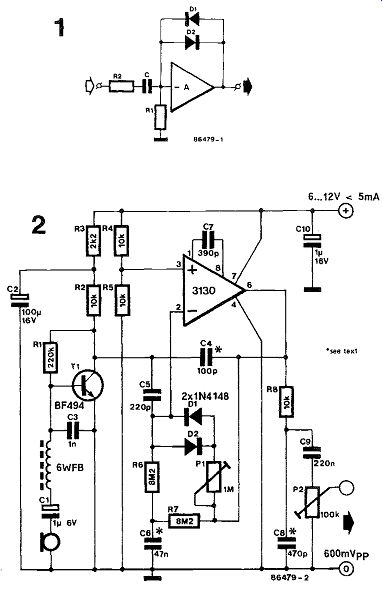
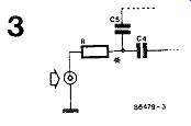
In the accompanying diagram, intermodulation distortion is reduced by signal-control of the cross-over point. The principle of operation is shown in Fig. 1.
The amplifier has a very high impedance input (value of R1 ). When the signal level is so low that the diodes do not conduct, the crossover point is determined by R1-C. As soon as the diodes conduct, the input impedance of the amplifier is reduced, which causes the cross-over point to shift up wards. The lower amplification of the frequencies is then smaller, and this enhances intelligibility. In fact, intelligibility of a signal processed in this manner is much better than a conventionally clipped signal.
The diagram in Fig. 2 shows the detailed realization of the principle. Transistor T1 is a microphone low-noise microphone preamplifier. The clipping circuit is based on A t: the limiting level is set by P1. The values of certain components depend on the application: guide lines are given in the table.
Application
C4 C6 C8
The diagram in Fig. 2 shows the detailed realization of the principle. Transistor T1 is a microphone low-noise microphone preamplifier. The clipping circuit is based on A t: the limiting level is set by Pi. The values of certain components depend on the application: guide lines are given in the table.
Application
C4 C6 C8
020 MINI AMPLIFIER
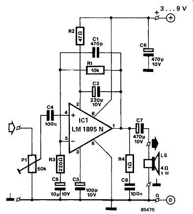
This little amplifier, operating from 3 . . . 9 V, and providing 1 W output into a 4 ohm loudspeaker, is one of those circuits of which you never have enough.
The amplifier is based on one 8-pin DIL IC type LM1895N. Electrolytic capacitors C2 and C6 de-couple the supply lines; C7 prevents d.c. reaching the loudspeaker; and C3 and C5 provide a low-impedance path to earth for audio frequencies.
The input signal is applied to pin 4 of the LM1895N via 131 and C4. Resistor R4 and capacitor Ca suppress any tendency to oscillation, i.e., improve the stability.
The amplification is determined by R., and R3: it is of the order of 50. Capacitor G, in parallel with Ri, ensures that the amplification drops off for frequencies above about 20 kHz. If the amplifier is in tended for use with a small AM receiver, it is desirable that the amplification starts falling off at a lower frequency. This is brought about by enlarging C1; for instance, if its value is doubled, the amplification starts dropping at 20/2 =10 kHz.
On the printed circuit board shown in figure 2 (which is not available ready made), 131 may be re placed by a wire link; the volume control is then carried out by an external logarithmic potentiometer connected to the PCB via a short length of screened audio cable.
Current consumption is 2.5 mA at 3 V or 7.5 mA at 9 V under no-signal conditions, and 80 mA at 3 V or 270 mA at 9 V under fully driven conditions: in the latter condition, the output power is 100 mW or 1 W respectively into 4 ohms.
The output power for different supply voltages and loudspeaker impedances can be estimated by deducting 1 V from the supply voltage, and raising the result to the power 2. Divide the number obtained by 8 and then again by the loudspeaker impedance.
The sensitivity of the amplifier is about 50 mV. This can be reduced by lowering the value of R1.
National Semiconductor Application.
--------------
021 MINI STEREO AMPLIFIER
This mini amplifier is based on the Thomson Type TEA2025. In this 16-pin DIL device hides a stereo amplifier that with a supply voltage of 9 V will provide 1 watt output per channel into a 4-ohm loud speaker. At full output, the input sensitivity is about 25 mV77. If this is too sensitive, a resistor R may be connected between pin 6 and C7 and between pin 11 and C2. The sensitivity then becomes (25 + 1/2R) mV, provided R >1 k Ohm. Furthermore, the supply voltage may lie between 3 V and 12 V.
The operation of the IC cannot be discussed here, but for those interested its internal circuit diagram is reproduced in Fig. 1. One useful feature of the TEA2025 is that it has a soft-start circuit on board, thus obviating annoying plops in the loudspeaker at switch-on.

Fig. 1. Circuit diagram of the mini amplifier.
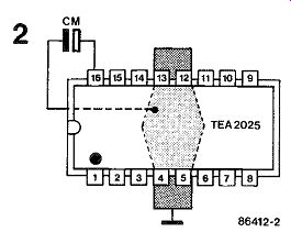
Construction of the amplifier is fairly simple, but has its peculiarities. First, there is the earth, which in this case should not be of wire, but rather consist of a metal earth plane (if you design your own PCB, this would be of copper). If at all possible, pins 4 and 5 as well as pins 12 and 13, should be connected to a (copper) area of not less than 5 cm'. The two areas should be connected in a suitable manner, and in such a way that a heat sink is formed under the IC as shown in Fig. 2. This ensures both good heat conduction and a good earth. Moreover, all other connections should, of course, be kept as short as possible. This is particularly important in the case of the supply lines, which should be decoupled by as close as possible to the IC. The negative terminal of this capacitor should be soldered direct onto the earth plane; the positive terminal is soldered in the normal manner to pin 16.
Finally, the distortion for a power output of about 0.25 W is roughly 0.3 percent.
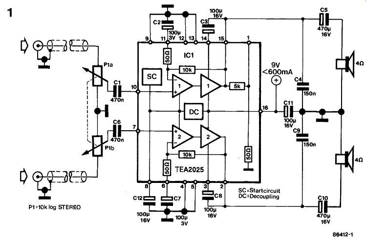
Fig. 2. This construction of earth plane cum heat sink is both practical and saves space.
022 MOSFET POWER AMPLIFIER
The output power of an operational amplifier is often increased by a complementary emitter follower. It can also be done with a MOSFET, but it is not a good idea to connect such a device as a complementary source follower because the maximum output voltage of the opamp is then reduced appreciably by the gate-source control voltage of the MOSFET, which can be a couple of volts.
Another approach is to connect two MOSFETs as a complementary drain follower. The (alternating) output current provided by the MOSFETs is limited by the level of the supply voltages and the saturation voltages of T3 and T4 Resistor R8, together with Rs, provides feedback for both the opamp and the MOSFETs. The open-loop amplification of the opamp is, therefore, increased by (1 +Rs/Rs). The closed-loop amplification of the complete amplifier is (1 +Rs/R2), i.e., 11.
The current source formed by T1 and T2 is required for arranging the quiescent current of T3 and T4 at 50 mA. The values of resistors R4 and R5 are such that, without the current source, the voltage drop across the resistors resulting from the direct current through the opamp is not sufficient to switch on T3 and T4 With the current source, and depending on the setting of 13-; the voltages across R4 and R5 rise, which increases the quiescent current through T3 and T4 In view of the temperature dependence of the quiescent current, T2 must be mounted on the common heat sink (c. 5 K/W) of the MOSFETs.
The output power is not less than 20 W into 8 ohm, at which level the harmonic distortion amounts to 0.075 percent at 100 Hz and to 0.135 percent at 10 kHz.
Source: Voice coil drives using complementary power MOSFETS by M Alexander in Motor-Con proceedings, April 1984

------------
023 NOISE GATE
Noise on an audio signal becomes more troublesome as the signal itself becomes smaller.
When a mixer is connected to a number of signal sources, it becomes particularly disturbing when one or more of these sources produce only noise. In these situations, a noise gate is a real help. Such a gate continuously monitors the level of the audio signal and switches it off, after a predetermined period, if the level drops below a preset value.
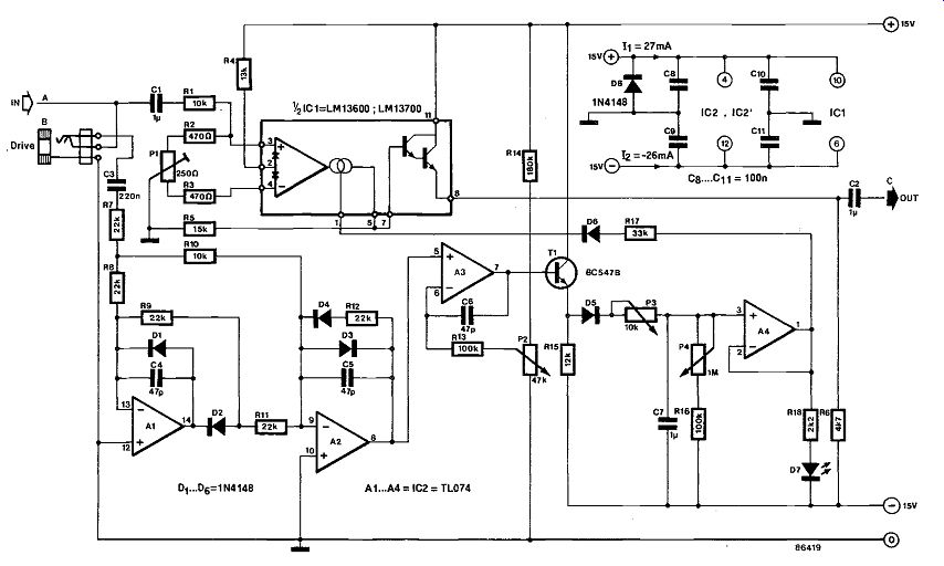
The circuit consists of two parts: a control section and a regulator section. The control section, based on opamps At to A4 incl., derives a voltage from the audio signal that is used to drive the regulator.
The regulator is a voltage-controlled amplifier, for which one of the two operational transconductance amplifiers contained in a Type LM13600 or LM13700 is used. For a stereo system, one control section and two regulator sections are required. For a double mono version, two control sections and two regulators are needed. One LM13600 or LM13700 will thus suffice for all these requirements.
Opamps A1 and A4 form a full-wave rectifying circuit. Opamp A3 compares the peak value of the signal with the direct voltage set by P2. If the peak value is larger, capacitor C7 is charged via Ti: the attack time is set by P3. The time lapse after which the audio signal is switched off is determined with P4. The control of the voltage-controlled amplifier (VCA) and the LED indicating whether there is a signal present is effected by A4. Diode D4 ensures that the amplification of the VCA is really zero when the output of A4 is low (i.e. less than -15 V).
The input of the regulator section has an impedance of about 10 k-O and is designed for audio signals of 1 Vrms. However, even for a 12 dB higher input signal, the distortion is still not greater than 1 percent. Where higher input voltages are the norm, the value of R1 should be altered accordingly. Where lower inputs are the norm, a preamplifier should be used.
It is, therefore, seen that the noise gate should preferably be connected between the preamplifier and power amplifier.
The output level is set with R5, while P1 enables the circuit to be adjusted for minimum switching noises. To this end, the drive input is switched on and off by Si, while the audio input remains open-circuit.
It is best to use a 3.5 mm chassis socket with break contact for the drive input: the break contact then replaces S1. As soon as the jack is inserted into the socket, the connection between the audio input and the regulator is broken.
This type of drive input affords a number of special effects, such as the switching in of, say, an echo unit at the command (sufficiently high signal level) of a given instrument (e.g. a snare drum). The command instrument is plugged into the drive input for this purpose, while the regulator is connected into the effects unit.
--------------43
024 SIMPLE PREAMPLIFIER
This design answers the need for an inexpensive, yet good quality, preamplifier equipped with a tone control section.
Fig. 1 shows the circuit diagram. The amplification of the input stage set up around opamp A1 is adjust able between 10 and 20 with preset P1 The 0 dB level at the input is 50 mV, while the input impedance and capacitance are 47 K-Ohm and 47 pF, respectively to enable ready connection of most record players and cassette decks. The tone control section is a standard Baxandall type with P3 and P4 as the respective bass and treble controls. The gain vs frequency curves for various settings of the tone controls appear in Fig. 2. Here the 0 dB level corresponds to 1V.

------------
------------
The current consumption of this preamplifier is modest at about 5 mA. When the circuit is correctly balanced, the indicated measuring points should all be very nearly at ground potential. The circuit shown here must, of course, be duplicated to obtain a stereo preamplifier.
025 SINGLE-CHIP 40W AMPLIFIER
To answer the need for a compact amplifier that is capable of satisfactory operation when driven from a compact disc player, Philips have developed the Type TDA1514 AF amplifier chip, which is remarkable for its excellent specifications, ruggedness and output power. The device is housed in a 9-pin SIL POWER enclosure which has a thermal resistance of less than 1.5 K/W, so that the heatsink required must have a thermal resistance of no more than 3.8 K/W if the chip is operated at its maximum dissipation of 19 W (Ub = ± 27.5 V, Ta = 50 °C).
The circuit diagram shows that very few components are needed to make this high-performance amplifier. The power supply to feed the chip must be capable of delivering a current of at least 3 A; the quiescent current demand of the amplifier as shown is about 60 mA. The supply voltage should not exceed ± 27.5 V.
Although this project is not supported by a ready made printed circuit board, you should not experience too much difficulty in constructing the amplifier if it is built on a piece of Veroboard. Make sure, however, that the tracks and connections to the supply and output terminals are as short as possible, and use double tracks where this is
necessary. In this context, it is advisable to fit decoupling capacitors C3 and C8 as close as possible to the chip supply pins. Resistors R2 and R3 deter mine the amplifier's closed loop voltage gain, which has a range of 20 to 46 dB.
Finally, some measurement data obtained with a prototype of the amplifier:
P. at Dtot = -60 dB;
Ub = ± 27.5 V; RL = 8 ohm: 40 W
S/N at P0=50 mW: 82 dB
Supply ripple rejection at f=100 Hz: 72 dB
Harmonic distortion at P0=32 W: -85 dB
Intermodulation distortion at P0=32 W: -80 dB 3 dB bandwidth at D_tot= -60 dB: 20-25 000 Hz Slew rate: 15 V/µs
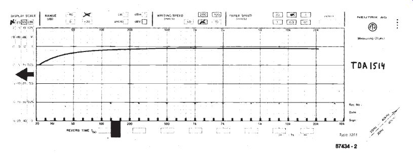
The gain vs frequency curve and the harmonic distortion table show that this amplifier provides very good sound reproduction at a considerable output power level.
Po= 10 Wrms
Total harmonic distortion level

------------
------------
026 SMD HEADPHONE AMPLIFIER
Although the use of SMDs (surface mount devices) is not yet widespread among electronics hobbyists, and the availability of these parts is still problematic in certain areas, there appears to be no way of stop ping the ever increasing miniaturization of chips and circuits. A good instance of this happening at an accelerating pace is the Type TDA7050 head phone amplifier, which used to be available in a standard DIL enclosure, but is currently only manufactured in SMA technology.
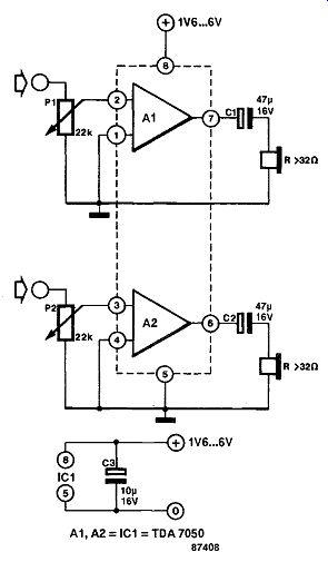
The Type TDA7050 is a complete stereo amplifier with a gain of 26 dB and an output power of 2 x 75 mW. As seen in the circuit diagram, two electrolytic capacitors are required to block the offset voltage at the amplifier outputs. It is also possible to set up the amplifier in a bridge configuration to obtain an output power of 150 mW: simply omit the capacitors, and connect pins 2 and 4 to ground.
Pins 1 and 3 are connected to form the amplifier's input, while the loudspeaker is connected between pins 6 and 7.
The current consumption of the chip at maximum output power is of the order of 100 to 150 mA, while the quiescent current amounts to a mere 5 mA. The amplifiers should be terminated in 3252, a common value for modern headphones. The supply voltage is normally 4.5 V, and pins 6 and 7 are at half the supply potential during quiescent operation.
-----------
027 SPEECH PROCESSOR WITH BACKGROUND SUPPRESSION
A speech processor is commonly used in public address installations and in utility transmitters. It augments the average value of the speech signal, so that in spite of a high level of background noise or, in the case of a radio transmission, a lot of interference, speech recognition remains possible. In many cases it is, however, undesirable that this background noise or interference is enhanced together with the wanted signal. A possible remedy, as outlined here, is to provide an adjustable threshold at which the speech processor becomes active.
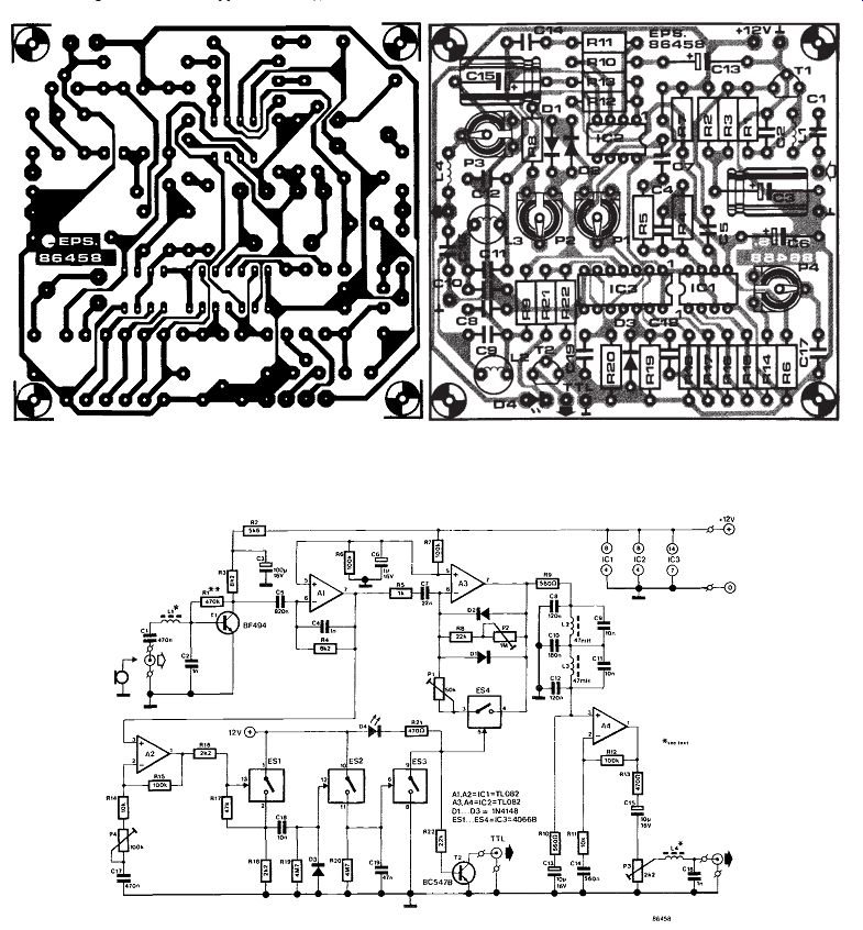
With reference to the diagram, the signal from the microphone is amplified in T (a low-noise amplifier) and in A1. Limiting (or clipping) of the signal takes place in A3.
The signal (taken from the output of A1) is also amplified in A2. When the output of this opamp reaches a certain level, electronic switch ES1 is actuated. Consequently, the monostable formed by ES2 changes state, and this closes ES3, whereupon ES4 is opened, which in its turn increases the amplification of A3. When ES4 is closed, the amplification of A3 is determined by the ratio P1:Rs; when the switch is open, by the ratio (P2+ R8):Rs.
The mono-time, determined by the time-constant R20-C19, has been chosen such that speech is not clipped. The low-pass filter between A3 and A4 ensures that frequencies above 3 kHz are severely attenuated. The required output level is set by P3.
Calibration is somewhat unorthodox: a signal source with a continuous output of speech by trained speakers is used. The microphone is positioned in front of the loudspeaker at normal speaking distance and the sound level adjusted to roughly the level of the user. Next, connect a pair of head phones to the output of the processor and make sure that only the output of these phones can be heard. Adjust P4 for maximum resistance, and then set the clipping level with P2 (which is a matter of personal taste). At maximum clipping level, intelligibility of the speech will remain good in the presence of interference, but it will have a somewhat harsh, metallic character. Then, adjust P: for maximum resistance, and P4 till all background noise disappears. Finally, set the ratio signal: background noise with Pi; this is best done by making a recording of the user's speech via the microphone and the processor. When the processor is active, i.e. clips, D4 lights.
L1 to L4 incl. are 6 turns 36 SWG CuL through 3 mm ferrite beads.
-------------
028 STEREO INDICATOR
On most FM tuners, the stereo indicator lights upon detection of the 19 kHz pilot tone. However, this need not mean that the program is actually stereophonic, since the pilot tone is often transmitted with mono programs also. A similar situation exists on stereo amplifiers, where the stereo LED is simply controlled from the mono-stereo switch.
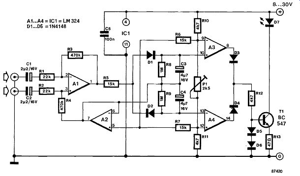
The LED-based stereo indicator described here lights only when a true stereo signal is fed to the in puts. Differential amplifier Ai raises the difference between the L and R input signals. When these are equal, the output of A1 remains at the same potential as the output of A2, which forms a virtual ground rail at half the supply voltage. When A1 detects a difference between the L and R input signals, it supplies a positive or negative voltage with respect to the virtual ground rail, and so causes C3 to be charged via D1 , or C4 via D2. The resistors connected in parallel to these capacitors ensure slow discharging to bridge brief silent periods in the program. Comparator A3-A4 switches on the LED driver via OR circuit D3-D4.
When building the circuit into an amplifier, care should be taken to select the right point from which the input signals are obtained. In general, this should be before the volume and balance controls, but behind the mono/stereo selector. The signal level should not be less than 100 mV to compensate for the drop across D1 or D2. Also observe that the impedance at the selected "tap" location is relatively low. Should the stereo light come on when a mono program is being received, the input signals are different, and the sensitivity of one of the amplifier channels should be altered. If this is impossible or undesirable, R3 may be replaced by a series connected preset and a resistor. The sensitivity of the stereo indicator is adjustable with Pt. The current consumption is less than 7 mA when the LED is off, and about 20 mA when it is on.
---------
029 STEREO PREAMPLIFIER WITH TONE CONTROL
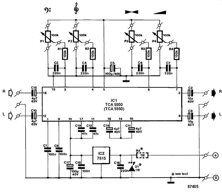
This simple, one-chip, stereo preamplifier is ideal for building into an existing AF power amplifier. It is based on a recently introduced integrated circuit, the Type TCA5500 or TCA5550 from Motorola.
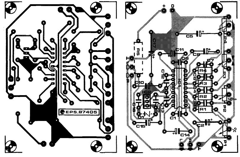
This double AF amplifier chip with inputs for balance, volume, and bass and treble controls forms a sound basis for a good quality preamplifier with a minimum of components. The onset points for the bass and treble controls are defined with C3 and C4 respectively. All (mono) potentiometers are best fitted direct onto the circuit board to make for simple mounting into a cabinet, and also to prevent hum and noise being picked up in the wiring that would otherwise be required.
The preamplifier has a current consumption of 35 mA, of which 5 mA is drawn by voltage regulator IC2. Zener diode D1 and power resistor Rs should be added if the positive supply voltage available in the power amplifier is more than about 30 V.
Specifications of the preamplifier:
Distortion: .0.1% at nominal output level.
Channel separation: a 45 dB.
Supply voltage: 8.8-18 V.
Tone control range: 14 dB.
Volume control range: >75 dB.
Maximum input voltage: 100 mV.
Amplification: 10.
Low output impedance.
Parts list:
Resistors (± 5%):
R1 … R4 incl. = 100K
R5 = see text
P1... P4 incl.=100K linear potentiometer
Capacitors:
C1; C9; C16 = 100n
C2; C8 = 10µ; 63 V; radial
C3;C4;Ce;C7;C18=220n
C5;C17=100µ; 40 V; radial
C10;C15=4µ7; 63 V; radial
C11;C14 =4u7; 40 V; radial
C12;C13=47 ohm
Semiconductors:
D1 = zener-diode 27 V; 1 W (see text)
IC, =TCA5500 or TCA5550 (Motorola)
IC2 = 7815
Miscellaneous:
PCB Type 87405
----------
---------
030 SUBWOOFER FILTER
------------
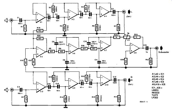

The filter described here is intended primarily for experimenting with a (central) subwoofer (see Ac Live Subwoofer, EE March 1986, p. 28). As the human ear cannot sense direction in a standing wave, directional sensitivity is generally poor at low frequencies, so that it would seem superfluous to use a stereo set-up below about 200 Hz. Therefore, the low frequencies can be concentrated on one good bass enclosure, which, of course, keeps the cost of the overall system down. The satellite loudspeakers (see EE, April 1986, p. 22) will then have to cope with the higher frequencies only.
The requisite crossover network described here is based on 24 dB/octave Bessel filters: the crossover frequency lies around 200 Hz. With reference to the circuit diagram, Ai and A2, buffer the left-hand and right-hand signals respectively. The high-pass filters for the two channels are formed by A3-A4 and A9-A10 respectively.
At the same time, the two channels are combined in As, and the resulting signal is passed through low-pass filter A6-A7. The amplification of A8 can be varied with Pi, so that the level of the low frequency signal can be matched to that of the high frequency signals. Note that the component values given in parentheses are the calculated values, with perfectionists may try to approach.
The power supply is a symmetrical design with short-circuit protection, which also prevents annoying "plops" at on and off switching.
If a different crossover frequency is required, refer to Active Crossover Network in the September 1984 (p. 28) issue of Elektor Electronics.
In the design stages, stability problems were en countered when opamps with JFET inputs (TL074; LF353, for instance) were used, whereas types with bipolar inputs, such as the NE5534 and the LM833, worked perfectly. The reason for the in stability in the JFET types is not known.
------
031 TRUE CLASS B AMPLIFIER
The quiescent current in this amplifier is always zero, so there is no need for zero setting or for a circuit to prevent thermal run-away. Complexity is further reduced by the use of a single supply voltage, Voltage divider R1-R2-R3 fixes the voltage level at the base of T1 at just above half that of the supply voltage. Since a current source, consisting of T3, R7, D1, and D2, has been included in the collector circuit of T2, this stage provides a very high voltage amplification. The return line of the current source is connected to the output, so that the voltage necessary to stabilize the source does not limit the dynamic push-pull characteristic. The current source has, therefore, a high-impedance character.
The complementary power amplifiers, T4 and Ts, are darlington transistors, which, of course, enable the collector current in the driver stage to be kept relatively low.
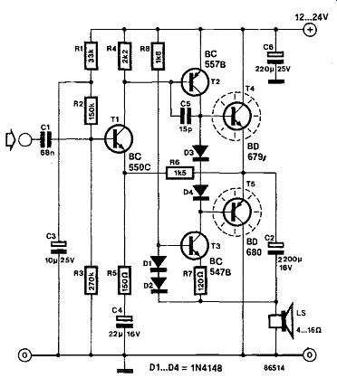
--------------- The feedback to the emitter of T1 via Rs and R6 determines the overall voltage gain, here 20 dB, and irons out any non-linear components.
Class B operation is normally obtained by direct interconnection of the bases of the power transistors.
In practice, this gave an overall distortion of not more than 0.16 percent (at a drive power of 0.25 W at 1 kHz). The simple addition of diodes D1 and D2 improved the distortion to not more than 0.1 percent. Note that these diodes do not alter the operation, because the Darlingtons have a relatively high base-emitter potential.
With a supply voltage of 12 V, the amplifier delivers some 2 W into 4 ohms (input sensitivity 200 mV), or rather more than 1 W into 8 ohms. A higher supply voltage will increase the output power (to a maximum of 10 W into 4 ohms at 24 V), but the power transistors then need cooling.
032 TUNING AF POWER STAGES
Simple, economically priced audio output stages, such as, for instance, those using the hybrid ICs in the STK series, may be improved in a simple manner as regards distortion, noise, and offset voltage.
To this end, the output amplifier is included in the feedback loop of an opamp. Fig. 1 shows the set-up for inverting output amplifiers, and Fig. 2 that for non-inverting ones (the normal situation).
In the calculations to arrive at the new gain of the output amplifier, determined by R, and R2, it is assumed that the LF356 provides an undistorted signal of 5 Vrms; note also that this type of opamp must work into a load of not less than 5 kiloohms to prevent distortion.
For an output power of 50 W into 4 ohms, the output stage must provide a voltage, U = PR =14.2 Vrms. If the amplification of the stage is 3, the opamp should deliver 4.73 V. For the set-up in Fig. 1, the value of R2 is then R2= 3R1, while for that in Fig. 2, R2 = 2Ri. Note that in both versions only the value of R1 should be altered. The total amplification may be calculated from the ratio of RA and Rs as follows: A = (RA + Rs)/Rs.
Furthermore, because of the load impedance of the op-amp, R, >10 k (Fig. 1); R2>10 k (Fig. 2); RA >10 52; and Rc >10 ohm (Fig. 1 and 2).
To compensate for the offset voltage of the output amplifier, the input capacitor should be replaced by a wire link. The capacitor in series with R, in Fig. 2 should also be short-circuited. The lower frequency limit of the complete circuit is then determined by Cs =1/2 pi f_lim Rs. The offset voltage is then smaller than 3 mV, provided both RA and Rc are equal to, or greater than, 100 k-Ohm. Where greater accuracy is required, 131 can be used to set the off set to exactly 0 V.
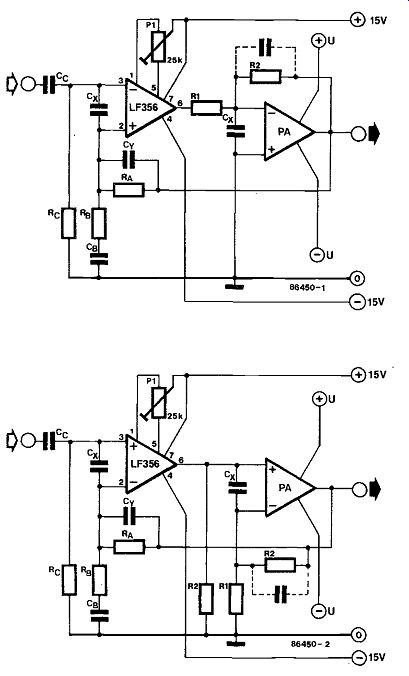
------------
To ensure that there is no direct voltage at the new input of the amplifier, capacitor Cc should have a value of Cc = 1/f_limRc.
Since the amplification of the output stage has been reduced to 3, its feedback factor has gone up, and the distortion has gone down. The additional feedback of the LF356 reduces the distortion even further. An overall reduction in the distortion from 1 percent to 0.1 percent is fairly typical.
The altered feedback unfortunately results in a change in stability. If there is a tendency to oscillate, the first thing to do is to bring the upper frequency limit back to its previous value with the aid of Cy =1/2 pi f_lim RA. If the tendency persists, capacitors Cx must be used: their value lies between 100 pF and 1nF. Our prototype (using STK ICs) worked satisfactorily without either Cx or Cy.