Learn how crystal-controlled oscillators produce precise, stable output frequencies by building the circuits.
By DAN BECKER
THE CRYSTAL-CONTROLLED oscillator has provided stable timing and frequency signals for years, and is now an integral part of products ranging from watches and computers to handheld transceivers and satellite receivers. First introduced in vacuum-tube form, most are now transistorized. The word quartz in advertising copy and specification sheets is the clue that they're inside. A time or frequency base derived from a resonating quartz crystal is the next best thing to a national time standard.
In the first installment of this two part series, resonators based on the piezoelectric effect were introduced. It was pointed out that a piezoelectric crystal produced electricity if it is subjected to physical stress and, conversely, the crystal is physically distorted if a voltage is impressed across its faces. Both properties are put to use in depth finder transducers.
In fact, the first practical application of a piezoelectric crystal was as a transducer to generate and receive sounds underwater for the detection of submarines during World War I. Later, crystal loudspeakers, microphones, and phonograph pickups were developed. The first quartz crystal controlled oscillator was introduced in the 1920's.
Synthetic or cultured quartz is now the dominant material of both crystal resonators and filters. The desired physical and electrical properties are obtained by cutting the quartz blank according to a set of strict rules. Packaged quartz crystal resonators are available as low cost catalog items, and if you can't find the frequency you need, you can order a custom made resonator.
All this is background to the subject of crystal-controlled oscillators. This article covers the fundamentals of all transistorized oscillator circuits, and includes five schematics and eight tables covering crystal-controlled oscillators complete enough for you to build your own circuits for personal instruction, experimentation or to meet a specific project requirement. All of the components are low in cost and readily available through retail stores or mail-order houses.
What is an oscillator? An oscillator is a circuit that generates a specific frequency and maintains that frequency within limits. A transistorized inductance-capacitance (LC) oscillator depends for its operation on the resonant interchange of energy between a capacitor and inductor for its operation; a transistor amplifier supplies pulses of energy of the proper phase and magnitude to maintain oscillations.
When used in oscillator circuits, transistors become converters that change DC electrical energy from the collector power supply into AC energy in the output circuit. The amplifying characteristic of the transistor maintains the circuit oscillations.
Two conditions are necessary to sustain oscillations. First, the feedback voltage from the collector circuit must be in phase with the original excitation voltage on the base-that is, the feedback must be positive or regenerative. Second, the amount of energy fed back to the base circuits must be sufficient to compensate for the energy losses that occur in the base circuit.
It is useful to review the concept of Q before discussing oscillator operation. Q is defined as a figure of merit in a resonant system. Equal to the reactance divided by the resistance, it represents the ability of the device or network to sustain oscillations with minimum feedback.
In short, the higher the Q the more efficient the resonator.
The intrinsic Q of quartz is 10 million at 1 MHz. Although the Q value for a mounted resonator crystal is reduced to levels of 20,000 to well over a million, it is still orders of magnitude better than the best LC resonator or tank circuit.
Crystal oscillator theory. The very high Q of a crystal oscillator significantly reduces frequency drift caused by temperature and power supply voltage variations. Moreover, crystal controlled oscillators generate less noise than conventional oscillators with LC tank circuits, so they have a purer output signal.
The simplest crystal oscillator consists of a single bipolar transistor with a simple feedback network. Figure 1-a shows a block diagram for a generic crystal oscillator. Here, an NPN amplifier is connected in three feedback circuits. Appropriate DC bias is assumed but not shown. Figure 1-b is an equivalent circuit with components L1 and C1, and C2 shown. All of the crystal oscillator circuits to be discussed here have the same basic topology, and include at least two capacitors and an inductor. The crystal can be considered to be part of the feedback circuit.
Capacitors C1 and C2 include residual transistor and junction capacitance. Capacitor C2 can be equivalent to a parallel combination of an inductor and a capacitor. This pair functions as the crystal's third overtone selector because it is capacitive only at the crystal's overtone frequency, and inductive at its fundamental. Thus, an inductor located at C2 prevents oscillation at the crystal's fundamental frequency.
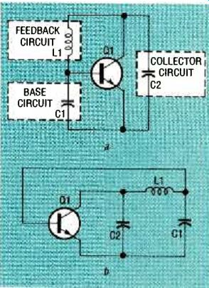
FIG. 1--BASIC CIRCUIT showing equivalent components, a and the circuit
redrawn to show a feedback network, b.
In addition to amplification and feedback, an oscillator requires limiting, which occurs when an increase in the input signal no longer produces an increase in the output signal. Thus, the oscillator's output reaches a limit and stays there.
Some oscillator circuits are named for a circuit characteristic such as electron-coupled or phase shift. However, many oscillators are named for their inventors: Among these are Butler, Colpitts, Hartley, and Miller. Five inventor-named circuit have been selected for this article; three are crystal-controlled versions of the Colpitts oscillator, one of the Pierce oscillator, and one of the Butler oscillator.
The standard Colpitts crystal controlled oscillator has rigid load and tuning requirements, while the two semi isolated versions are less temperamental, and are recommended as better choices for general purpose applications. If you want very precise output frequency, the Pierce crystal oscillator is your best bet. However, if you want to experiment with oscillators, you'll find that the Buller circuit oscillates even without a crystal, you can observe the results with the crystal in or out. Table 1 compares the characteristics of each of these circuits.
Colpitts oscillators
Two versions of the Colpitts crystal controlled oscillator are presented here: the standard and the semi-isolated. The standard circuit, shown in Fig. 2, is sensitive to variations in both crystal and load resistance. In addition, its output power is limited to less than half of the crystal's power dissipation. But, it's still a popular circuit.
Resistors R1, R2, and R3 DC bias transistor Q1. Potentiometer R2 allows up to about 1.5 milliamperes of emitter current. Capacitors C3, C4, and C6 bypass radio frequency at XTAL1's operating frequency (fundamental or overtone). Capacitor C2 functions like the feedback base circuit capacitor C1 in Fig. 1. At XTAL1's operating frequency, L1 and C5 have a net capacitive reactance, and thereby form collector circuit feedback capacitor C2.
For overtone crystals, L1 and C5 act like an overtone selector, preventing oscillation at the crystal's fundamental frequency. 'Primmer capacitor C1 fine tunes feedback element L1. As the value of C1 is made smaller, the oscillator's output frequency increases.
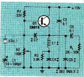
FIG. 2--A STANDARD COLPITTS crystal controlled oscillator.
To organize a standard Colpitts oscillator for your specific output frequency requirements, refer to Table 2. Note that frequencies from 1 MHz to 30 MHz are obtained with the fundamental mode, and frequencies from 35 to 60 MHz are obtained with a third-overtone crystal. The values for C2, C4, and C5 are given in picofarads, and the values for L1 are given in microhenries.
Semi-isolated Colpitts
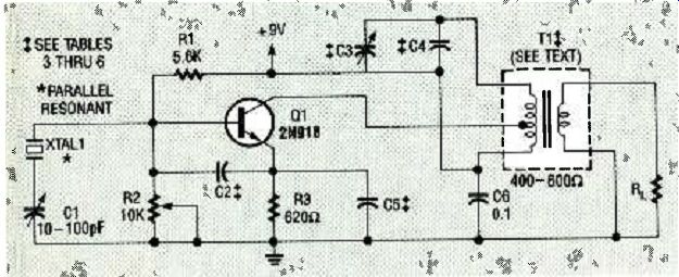
FIG. 3--A SEMI-ISOLATED COLPITTS OSCILLATOR with a fundamental-mode,
parallel resonant crystal.
Two versions of the semi-isolated Colpitts oscillator are described here. The first, shown in the Fig. 3 schematic, includes a fundamental-mode crystal. The second, shown in Fig. 4, is the same as that shown in Fig. 3 except that it includes overtone selector L1, C6 and radio-frequency bypass capacitor C3. Its operation requires a third overtone crystal.
In both circuits, RF transformer T1 takes an output signal from Q1's collector current, but T1 is not part of the oscillator's feedback network. In addition, the output power is up to 100 times the crystal's power dissipation. Therefore, 15 milliwatts of output can be obtained with only microwatts of crystal dissipation! Moreover, if the output transformer is tuned to a harmonic of the oscillator's frequency, the RF load current is effectively isolated from Q1's fundamental RF current. Therefore, variations in the load or T1 do not affect oscillator tuning.
For example, if a 10-MHz crystal is used, the RF transformer can be tuned to 20 MHz, 30 MHz, 40 MHz, or higher MHz. Thus the circuit has its own built-in buffer that can drive low impedance loads without detuning the oscillator.
However, as with the standard Colpitts circuit, the crystal is shunted by the emitter-base junction of the transistor--a low impedance. This lowers the oscillator's Q from tens of thousands to a few thousand, reducing its frequency stability. However, for most practical applications its stability is more than adequate.
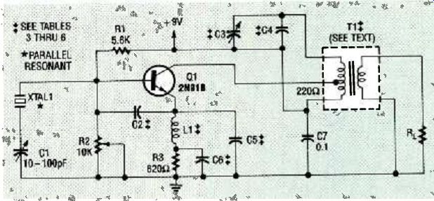
FIG. 4--A SEMI-ISOLATED COLPITTS OSCILLATOR with a parallel resonant
crystal and overtone selector.
Refer to the schematics shown in Figs. 3 or 4. In both circuits, resistors R1, R2, and R3 apply DC bias to transistor Q1. RF bypass capacitor C6 grounds one end of T1's primary. Capacitors C2, C5, and crystal XTAL1 form a feedback network as discussed earlier in reference to Fig. 1. Trimmer capacitor C1 serves the same function as it does in the standard Colpitts circuit. Transformer T1 and trimmer capacitor C3 (with C4) form a parallel resonant tank tuned to the desired output frequency.
If the output frequency is to be the same as the crystal's frequency, use the component values given in Table 3 or Table 5.
(Tables 3 through 6 contain specifications information on winding transformer T1, which is explained under the Construction section) In this case, the oscillator, the load, and T1 are all tuned to the same frequency, and each affects the tuning of the other. (The load resistor RL should initially be a 1/4-watt resistor). If the output frequency is to be a harmonic of the crystal's frequency, use the component values given in Table 4 or table 6. As mentioned earlier, this arrangement isolates T1 and the load, enabling the circuit to work with a wide range of load impedances.
The semi-isolated Colpitts oscillator shown in Fig. 4 requires a third-overtone crystal. Therefore, L1 and C5 appear capacitive at the third overtone, but they appear inductive at the crystal's fundamental frequency; together they form the collector circuit feedback element C2 shown in Fig. 1. Capacitor C6 bypasses DC-bias resistor R3, but it is most effective at the overtone rather than the fundamental frequency.
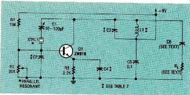
FIG. 5--A PIERCE CRYSTAL-CONTROLLED OSCILLATOR with a parallel resonant
crystal.
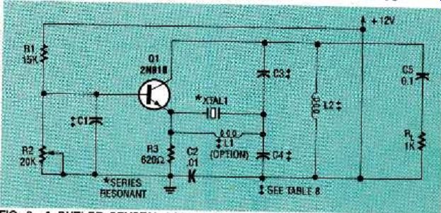
Fig. 6 ... Butler xtal-controlled osc. with a series-resonant crystal.
Pierce oscillator.
The best feature of the Pierce crystal oscillator, shown schematically in Fig. 5, is its very high operating Q. That very high Q is maintained because the crystal is connected between Q1's base and collector (a high impedance). This oscillator provides a very stable and accurate output frequency up to about 75 MHz. It is possible to tune this oscillator to within a few hertz of the desired frequency and expect it to remain stable there (when held at constant temperature). If an oven-controlled crystal is used, frequency change will only be several hertz over a wide temperature range. However, the Pierce oscillator does not offer very high output power. Moreover, it requires a very high load resistance of about 3000 ohms.
Resistors R1, R2, and R3 establish the DC emitter current.
Capacitor C5 bypasses RF at all frequencies, while C4 bypasses RF current at the desired operating frequency (fundamental or, overtone only). Capacitor C2 is base circuit feedback element C1 as shown in Fig.1, and the parallel network of C3 and L1 yields a net capacitive reactance at the operating frequency and is analogous to collector circuit feedback element C2 as shown in Fig. 1. Crystal XTAL1 forms feedback inductor L1 of Fig. 1, and as with the Colpitts oscillator, trimmer capacitor C1 fine tunes the circuit's operating frequency.
The component values of the Pierce oscillator also depend on frequency and are given in Table 7. Note that a fundamental mode crystal permits frequencies from 1 to 25 MHz, while a third-overtone crystal is required for output frequencies from 30 MHz to 75 MHz.
If a load resistance of the Pierce crystal oscillator is to be less than several thousand ohms, a 1to 5picofarad coupling capacitor must be used at C5 to prevent the low resistance of the load from detuning the circuit and preventing circuit oscillation.
Butler oscillator
A schematic of a Butler crystal oscillator is shown in Fig. 6. The Butler oscillator demonstrates what is known as input resistance limiting. Transistor Q1's DC emitter current is directly proportional to the strength of the radio frequency input signal; in addition Q1's RF-input resistance of approximately 40 ohms is inversely proportional to the DC emitter current.
Therefore, as the RF feedback increases, Q1's DC emitter current increases, but its RF-input resistance decreases. As Q1's RF-input resistance decreases, its RF gain also decreases, and this causes the output signal strength to reach a plateau.
The Butler oscillator's crystal circuit operates at series resonance, making it look resistive in the circuit. It is possible to substitute a 47-ohm resistor for the crystal and tune the circuit to a wide range, of frequencies with variable inductor L1. But the circuit is so sensitive to variations in load resistance that a fixed resistive load must be connected to its output.
Resistors R1, R2, and R3 set the DC emitter current. Bypass capacitors C1, C5, and C2 place transistor Q1 in a common-base configuration, couple the collector to the load, and bypass the positive supply lead, respectively. The feedback elements consist of capacitors C3 and C4, and inductor L2. The capacitors act like the base and collector elements C2, and C1 and inductor L2 act like the feedback circuit L1 in Fig.1.
Crystal XTAL1 feeds some of the RF output energy back into the emitter. Because the crystal behaves like a narrow bandpass filter, the emitter current forms clean sine waves that are low in harmonics. Inductor L1 cancels the detuning effects of the crystal's static capacitance C. However, if you build this circuit, get it to oscillate first without L1. Then, after it is working, install and fine tune L1 to obtain a precise output frequency.
Table 8 gives the values of the components in Fig. 6 that are shown without values. Note that a third-overtone crystal is necessary to obtain output frequencies from 20 to 55 MHz, while a fifth-overtone crystal is needed to obtain output frequencies from 60 to 100 MHz.
Selecting components
Remember that many common passive electronics components such as capacitors, resistors, and inductors that perform well at audio frequencies become inefficient and lossy in the radio frequencies.
For example, the parasitic inductance of a wirewound resistor can be significant in a radiofrequency circuit. Keep this in mind when selecting oscillator components.
Power-supply regulation is important for stable oscillator operation. Low-Q oscillators that are tunable over a wide range of frequencies require very stable, low-noise supplies, but that is not a requirement for high-Q crystal-controlled oscillators because they are generally immune to voltage spikes and noise. Thus, while regulation is important, it can be obtained with low-cost integrated circuit regulators.
Even with minimal regulation, it is recommended that the power supply positive voltage lead be bypassed with a 6 to 10 microfarad tantalum capacitor and a 0.01 microfarad ceramic disc capacitor. Capacitors suitable for RF bypassing and tuning should have Q values of 100 or more, and most general purpose ceramic disc capacitors meet that requirement.
The crystal oscillators described here need only one bipolar transistor. In general, any NPN transistor with a gain bandwidth product of at least 650 MHz is suitable. Possibilities include the 2N918 (shown in all of the circuits in this article), the MPSH-10, and the 2N2857. The 2N918 is available in plastic packages and metal cans. If you use 2N918's in metal cans, be sure to ground their cases. For frequencies below 50 MHz, a 2N3904 switching transistor will perform satisfactorily.
Inductor variety
Two basic kinds of inductors (tuning coils) are generally available: air wound, and core wound. Most are wound from number 20 to 40 AWG enamel coated magnet wire. Inductors for RF circuits usually have both magnetic and electrostatic shielding. This is obtained by winding the coil on an iron powder core, and then enclosing the assembly in a small metal can.
Core-wound inductors offer high Q's, good temperature stability (usually ± 200 ppm / °C), and are small. Powdered-iron core materials are often mixed with other materials to make special powdered-iron alloys.
Each is formulated to yield a sigh Q and optimum temperature stability over a specified frequency range. Oscillators or tuned circuits usually require Q's between 60 and 120. Before selecting a coil, examine the manufacturer's data to verify the coil's Q and usable frequency range.
Winding transformers
You can make your own radio frequency transformer T1 for the semi isolated Colpitts crystal oscillators shown in Figs. 3 and 4 from the toroidal cores and magnet wire specified in Tables 3 through 6. Under the column heading T1 (primary) these tables give the total number of primary turns, the wire gauge, and the designation for the appropriate core (e.g. T-80-2, T-50-2, T50-10, T-50-17). The first letter in this core code, T, stands for toroid, and the first number stands for the core outside diameter in fractions of an inch (e.g. 80 = 80/100 inch, 50 = 50/100 inch). The third number in the code designates a specific powdered iron composition.
When winding wire on the core, first wind on approximately 12.5% of the total primary turns on the core (or three turns, whichever is larger). Then make a tap by twisting together several inches of wire to form a loop, and continue winding until all the primary turns have been wound. The loop can then be formed into a tap by cutting the loop and scraping the insulation off of the ends. This tap is then ready to be connected to Q1's collector as shown in Figs. 3 and 4 and soldered during the circuit assembly procedure.
The secondary of transformer T1 should reflect the load impedance shown on the schematics of Figs. 3 and 4 (at the primary's tap). The turns ratio between the secondary and the primary's tap should be the square root of tap resistance divided by load resistance. The secondary winding can be wound from the same gauge wire as the primary.
For example, to reflect a tap resistance of 500 ohms, a 50ohm load would require a primary-tap to secondary-turns ratio of 3.16:1 (the square root of 500 divided by 50). Therefore, if the primary tap consists of three turns, use a one turn secondary. After you find that the circuit oscillates with the initial transformer, you can experiment by substituting other transformers with different turns ratios.
Oscillator construction
Carefully designed printed circuit boards are preferable to standard perforated boards as substrates for radiofrequency oscillators to minimize noise and interference. When building radiofrequency circuits, it is important that all components be inserted so they lie as close as possible to the board.
Use coaxial cable or TV twin lead to conduct high frequency signals for any distances over an inch. RCA-type audio connectors work well up to frequencies of 30 MHz, but BNC, F, and equivalent 50or 75-ohm connectors should be used at the higher radio frequencies.
The Colpitts and Pierce crystal controlled oscillator circuits discussed here include parallel resonance crystals, but the Butler oscillator has a series resonance crystal. In all circuits the crystal's load capacitance rating can be from 12 to 32 picofarads.
However, the higher frequencies require a smaller load capacitance so the crystal will provide enough inductive reactance to prevent oscillation above the desired frequency. Therefore, a 12 to 20 picofarad load capacitor should be used in circuits expected to operate at frequencies above 15 MHz.
After building the standard Colpitts oscillator, and before trying it for the first time, set variable capacitor C1 to its maximum capacitance value. The following start-up directions apply to all Colpitts oscillators and the Pierce oscillator, but not the Butler oscillator: Initially, couple a 4.7 K ohm resistor to the 0.1 microfarad load-coupling capacitor (C6 in Figs. 2 and 5). Adjust trimmer potentiometer R2 until the circuit oscillates. When the circuit is oscillating properly, a different load resistor value can be substituted. For 0.1 microfarad load-coupling capacitors, RL must be a resistive load of 2 to 10 K ohms For coupling a low impedance load, use a 1 to 47 picofarad capacitor.
If the output frequency is to be the same as the crystal's resonant frequency, refer to the component values given in Table 3 or Table 5. In this case, the oscillator, the load, and T1 are all tuned to the same frequency, and each affects the tuning of the other. Therefore, a ¼ watt resistor should be inserted initially at R,. After completing the Pierce oscillator, lightly couple a radio frequency or oscilloscope probe to Q1's collector with a 5 picofarad capacitor. Then carefully adjust trimmer potentiometer R2 until the circuit oscillates properly.
As stated earlier, a 47-ohm resistor can be substituted for the crystal in building the Butler oscillator. The circuit can be tuned to a wide range of frequencies with the variable inductor L2. Be sure to keep a fixed resistive load connected to the oscillator's output because it is sensitive to variations in load resistance.
It was also stated earlier that a second optional inductor L1 will cancel the detuning effects of the crystal resonator's parallel capacitance C1, Complete the construction and make sure the circuit oscillates before installing L1 and fine tuning it.
Also see: Crystal Oscillators [Part 1]