Understand resistive-capacitive filters and learn how to use them in your projects and experiments.
By RAY MARSTON
THE TERM FILTER DESCRIBES a wide variety of frequency-selective circuits. Certain frequencies pass through a given filter while others are attenuated.
There are four basic filter types: low-pass, high-pass, bandpass, and band rejection or notch. Filters composed of resistive (R), inductive (L), and capacitive (C) elements are called passive filters. Active filters include high-gain operational amplifiers with passive filter feedback networks.
Filter circuits that contain only resistors and capacitors are called resistive-capacitive (RC); those that contain only inductors and capacitors are called inductive-capacitive (LC). Filter circuits generally combine inductive and capacitive components because inductive reactance increases with frequency, and capacitive reactance decreases with frequency.
The two opposing effects permit many possibilities in all filter design.
However, this article will focus on RC filters and applications. Later articles will review LC filters and look at active filters in greater detail. The big advantage of active filters is that they do not require inductors, which can be large and heavy at low frequencies. Active filters need only R and C components, but they require some kind of power supply.
A capacitor by itself has inherent filtering capability for alternating current because capacitive reactance, Xc, is inversely proportional to frequency
fe = 1 /2 pi RC
It blocks direct current completely and opposes the passage of low-frequency signals although signal passage becomes progressively easier as frequency increases.
Low-pass and high-pass
Filters contribute to the operation of many different circuits by screening out unwanted frequencies and allowing only the wanted ones to pass. Resistive-capacitive filters are better suited for low-frequency filtering (up to 100 kHz), whereas inductive-capacitive filters are better suited for high-frequency filtering (above 100 kHz). Figure 1-a is the circuit of a simple RC, low-pass filter that passes low-frequency signals but rejects those with higher frequencies. Resistor R1 is in series with the load, and capacitor C1, the reactive element, shunts the load. This filter exhibits a gradual rolloff beginning at the upper cutoff frequency where capacitive reactance equals the value of resistor R. Because it is a low-pass filter, there is only one cutoff frequency, and it can be determined by the formula:
f = 1 /2 pi RC = 1/6.28RC = 0.159/RC
The cutoff frequency (f_c) is that frequency at which the signal output voltage is 6 decibels (dB) below its peak level.
Table 1 lists the formulas for determining fc, R, and C for the schematics in this article that do not include component values. In these formulas 2n has been converted to the number 6.28.
The cutoff-frequency can also be measured at the half-power points as shown in Fig. 1-b.
These are at 70.7% of the peak power with the real power dissipated at 50% of maximum. The half-power point is the upper cutoff frequency of a low-pass filter.
High-pass filter
The high-pass filter passes high frequencies and opposes or blocks the passage of low frequencies. As shown in Fig. 2a, the simplest high-pass filter consists a single capacitor in series with the load and a resistor that shunts the load. Capacitor C1 opposes current flow that varies inversely with frequency.
The higher the frequency, the smaller the opposition, measured in ohms. The filter completely or partially blocks signals at low frequencies, but permits their passage as frequency increases.
Figure 2-b shows the positive slope at the high-frequency end of the frequency vs. gain response curve for a high-pass filter. The pass band is defined as the area under the curve and the stop band is the area to the left of the curve.
The high-pass filter cuts off or blocks all frequencies below the cutoff frequency, fc, permitting all those above that frequency to pass. The half-power (-3dB) point of a high-pass filter is the lower cutoff frequency. Both high-pass and low-pass filters have just one cutoff point, but as will be explained later, both bandpass and band-reject (or notch) filters have two cutoff frequencies.
Both of the filter circuits shown in Figs. 1-a and 2-a have a single RC stage and are known as a first-order filters. If a number (n) of these filters are cascaded, they will form what is known as an nth-order filter.
Phase-shift oscillator
Filters can be effectively cascaded by including them in the feedback networks of operational amplifiers. Figure 3 is a circuit for a third-order, high-pass filter that converts an opamp into a phase-shift oscillator. The filter is inserted between the output and the input of the inverting (180° phase-shift) amplifier.
The filter will provide this phase shift at a frequency of about 'ha of the product of R and C. Thus the complete circuit has a loop shift of 360°, and it will oscillate at this frequency if the op-amp has sufficient gain.
An op-amp with a gain of about x 29 will compensate for filter losses and yield a loop gain greater than one.
Figure 4 is a schematic for an 800-Hz phase-shift oscillator.
Potentiometer R4 must be adjusted to give a clean output sinewave and potentiometer R6 will vary the output gain.
Bandpass filter
A bandpass filter passes a specified frequency band while rejecting adjacent frequencies above and below that passband.
A bandpass filter can be made by combining (or cascading) a high-pass filter with a low-pass filter as shown in Fig. 5-a so that a band of frequencies not stopped by either filter is passed.
A typical bandpass filter response curve, as shown in Fig. 5-b, has a generally trapezoidal shape with a positive slope on the low frequency (left) end indicating the limit of the high-pass stopband and a negative slope on the high frequency (right) end defining the low-pass stopband. The flat top of the curve (0 dB) indicates constant signal gain.
The bandwidth of the filter is the frequency difference between the half-power, or -3dB points. These are the points ...
TABLE 1
FORMULAS FOR DETERMINING FILTER COMPONENT VALUES
High- and Low-Pass Filter (Figs. t to 5)
Balanced Wien Tone Filter (Figs. 6 to 10)
'Win-T Notch Filter (Figs. 11, 14, and 15)
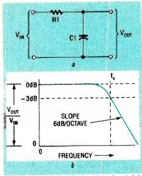
FIG. 1-LOW-PASS RC FILTER circuit (a), and frequency response curve
(b).
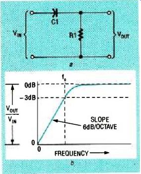
FIG. 2-HIGH-PASS RC FILTER circuit (a), and frequency response
curve (b).
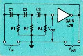
FIG. 3-THIRD-ORDER HIGH-PASS filter as a component in a phase-shift
oscillator.
... where the filter response is 3 dB down from the maximum point on the curve. The bandwidth is between fil (high pass and fc2 (low pass). The formula for bandwidth is:
Bandwidth in hertz = f.2-frl
The passband of a filter is the range of frequencies that pass through the filter. Insertion loss is the loss of signal strength experienced by the frequencies in the passband passing through the filter. If the filter were absent, and the source and load were connected directly to each other, the output signal would increase by the amount of the insertion loss.
Figure 6-a is a special band-pass filter called the Wien-tone filter made by cascading a low-pass and a high-pass filter with the same cutoff frequencies.
This permits the filter to select tones with minimum attenuation at a single frequency.
Resistors R1 and R2 have the same values and they are equal to the capacitive reactances of C1 and C2 at the desired cutoff frequency. The Wien-tone filter is called a balanced filter, a term that always means with respect to ground.
Figure 6-b is the frequency-response curve of the balanced Wien-tone filter with an attenuation factor of 3 (-9.5 dB) at L. The circuit's principal feature is its ability to shift input signal phase + 90° and-90 °, and set it precisely at theft of 0° as shown in the phase-shift curve Fig. 6-c.
This filter can be combined with an operational amplifier to ...
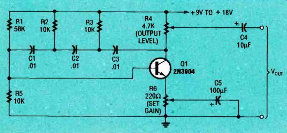
FIG. 4--PHASE-SHIFT OSCILLATOR produces 800Hz sinewaves.
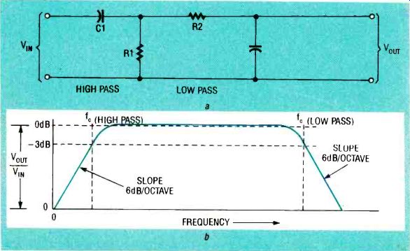
FIG. 5--HIGH-PASS AND LOW-PASS FILTERS cascaded to make a bandpass
filter (a), and frequency response curve (b).
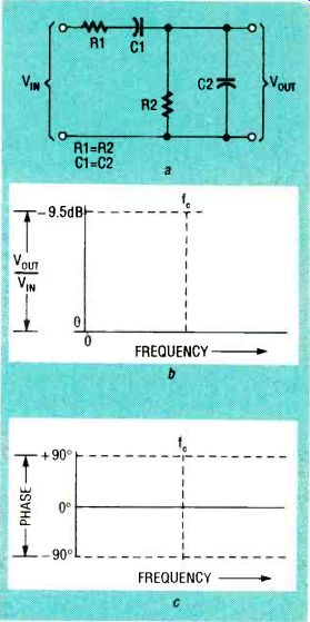
FIG. 6--BALANCED WIEN-TONE FILTER (a), frequency-response curve
(b), and phase-shift curve (c).
... become a sinewave oscillator as shown in Fig. 7. The output of the non-inverting amplifier with a gain of about x 3 is fed back to its input through R1 and C1 to give a unity loop gain.
Band-reject filter
A band-reject or notch filter has a function that is the inverse of the passband filter. It is able to reject one specific frequency, the stopband, but pass all others. Figure 8-a shows a band-reject filter that is a modification of the circuit shown in Fig. 7.
In this circuit resistors R2 and R4 divide the voltage with a nominal attenuation factor of 3.
As a result, the voltage divider and Wien filter outputs are identical at f, and the output, which equals the difference between the two signals, becomes zero.
The Wien bridge band-reject filter network can close a loop around a high-gain operational amplifier to form an oscillator as shown in Fig. 9-a. It might appear that the Wien filter's output is fed to the input of the high-gain amplifier that has its output fed back to the Wien filter's input to complete a positive feedback loop.
However, if the circuit is redrawn as in Fig. 9-b, it is clear that the op-amp actually functions as a x 3 non-inverting amplifier, and that the circuit is similar to that shown in Fig. 7.
Some form of automatic gain control will be needed if high-quality sinewaves are to be generated from this circuit.
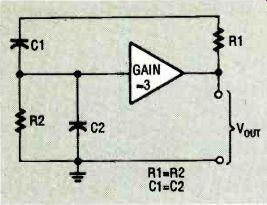
FIG. 7--BASIC WIENFILTER-BASED oscillator.
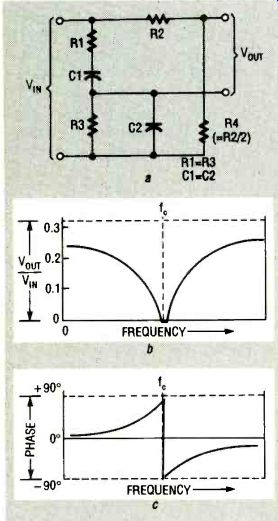
FIG. 8--WIENBRIDGE NOTCH FILTER (a), frequency-response curve (b),
and phase-shift curve.
FIG. 9--THE WIEN-BRIDGE OSCILLATOR (a) is the equivalent of the
oscillator shown at (b).
The tuned frequency of the Wien bridge network can be changed by simultaneously altering its two resistor or capacitor values. Figure 10 is the schematic for a wideband (15 Hz to 15 kHz) variable-notch filter.
Ganged potentiometer R3 and ganged switch S1 permit fine tuning and decade switching and trimmer potentiometer R6 performs null trimming.
Twin-T filter
Figure 11-a is a schematic for a twin-T notch filter. A prime advantage of the filter is that its input and output signals share a common-ground connection, and its off-frequency attenuation is less than that of the Wien bridge filter. However, it also has a drawback: To work effectively, the values of all three resistors (and the capacitive reactances at a specified frequency) must be varied simultaneously. This filter is balanced when its components have the precise ratios shown in Fig. 11-a. For perfect nulling, the R1 /2 resistor value must be carefully adjusted.
The distinctive notched frequency-response curve for the balanced twin-T filter is shown in Fig. 11-b. Notice that at f_c the notch has a value of zero. The abrupt phase shift curve is shown in Fig. 11-c. The filter has zero phase shift at fer, but that phase shift changes sharply to + 90° or-90° for slight variations above and below f . Both the balanced twin-T and the Wien bridge filter have very low effective Q's. The value Q is calculated by dividing the value off, by the bandwidth between the filter's two -3 dB points. A typical value for a twin-T filter is 0.24. The filter attenuates the second harmonic off, 9 dB. By contrast, an ideal notch filter would not attenuate the input signal.
This shortcoming of the twin-T filter can be overcome by "bootstrapping" the common terminal of the filter, as shown in simplified block diagram Fig. 12. High effective Q values can be obtained with this circuit, and attenuation of the second harmonic off will be negligible.
An explanation of how a balanced twin-T filter works can be quite complicated, so the equivalent diagram Fig. 13 is presented here to simplify that explanation. The filter has been resolved into a parallel-driven, low-pass filter (fe/2) and a high-pass filter (2fr) whose outputs are connected to an RC voltage divider (fe). This output divider loads the two filters and affects their phase shifts.
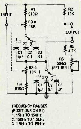
FIG. 10--VARIABLE-FREQUENCY, Wien-bridge notch filter (15 Hz to
15 kHz).
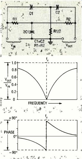
FIG. 11--BALANCED TWIN-T NOTCH FILTER (a), frequency-response curve
(b), and phase shift curve (c).
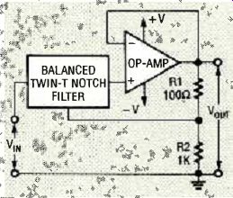
FIG. 12--BOOTSTRAPPED HIGH-Q notch filter.
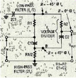
FIG. 13-EQUIVALENT CIRCUIT DIAGRAM of the balanced twin-T filter.
As a result, the signals at points A and B are identical in amplitude,
but have phase shifts of -45° and +45° respectively at f.
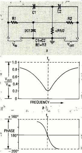
FIG.
14--NEGATIVELY UNBALANCED TWIN-T FILTER provides a 180° phase
shift at fc (a), its frequency response curve (b), and phase-shift
diagram (C).
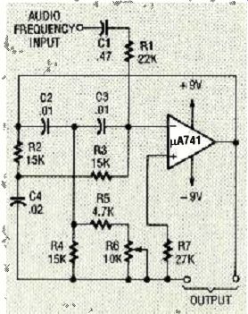
FIG. 15--A 1 KILOHERTZ OSCILLATOR/ ACCEPTANCE FILTER based on a
negatively unbalanced twin-T network.
At the same time, the impedances of the R and C sections of the output divider are equal and introduce a 45° phase shift at L. Thus the divider effectively cancels the two phase differences and gives a precise output of zero, the phase-cancelled difference in amplitudes between the two signals.
Therefore, a perfectly balanced twin-T filter has a zero output and zero phase shift at L. As shown in Fig. 11-c, if the frequency is slightly below ff, the output is dominated by the response of its low-pass filter, and is shifted in phase by-90 °; at frequencies above f , the output is dominated by the response of its high-pass filter, and is shifted in phase by + 90 °, An unbalanced version of the twin-T filter can be made by changing the value of the R1 /2 resistor to one that is not ideal.
If this resistor has a value greater than R1 /2, the circuit will be positively unbalanced. It will act the same way as was just described, but its notch will have limited depth (it will not reach zero). However, it still offers a zero phase shift at f . If, by contrast, the resistor has a value less of than R1 /2, the circuit, as shown in Fig. 14-a, will be negatively unbalanced.
It will also give a notch of limited depth, as shown in Fig. 14-b, but it has the useful characteristic of being able to produce output. There will be a 180° phase shift at ff, as shown in Fig. 14-c.
Figure 15 is a schematic of a negatively unbalanced twin-T notch filter that can be a component in either a 1 kHz oscillator or a tuned acceptance filter. The twin-T filter is connected between the input and output of the high-gain inverting amplifier so that an overall shift of 360° occurs at ff.
The circuit will oscillate if potentiometer R6 is adjusted so that the twin-T notch gives enough output so the system has an overall gain greater than unity.
To convert the circuit to a tone filter, adjust trimmer potentiometer R6 to give a loop gain that is less than unity, and feed an audio input signal through C1 and R1. Under this condition, R1 and the twin-T filter interact to form a frequency-sensitive circuit that gives high negative feedback and low gain to all frequencies except fc. The circuit gives little negative feedback and high gain at f. Trimmer potentiometer R6 can vary the sharpness of the tuning.
Also see: Link | --HARDWARE HACKER