The bipolar junction transistor is the cornerstone of modern solid-state electronics. Learn (or review) the basics of this important active device.
By RAY MARSTON
THE BIPOLAR JUNCTION Transistor (BJT) triggered the revolution in modern solid-state electronics in the 1960's. Although the discrete small-signal BJT has since yielded to the integrated circuit in economic importance, it lives on in the form of discrete linear and switching power transistors as well as radio-frequency transistors into the microwave region.
The principles behind the operation of the BJT are important to the understanding of many of today's most popular linear and digital integrated circuits. Moreover, the transistors in the digital logic transistor families-TTL, Shottky TTL, and emitter-coupled logic (ECL) are BJT's.
This article focuses small-signal BJT's and practical circuits that can be made with them.
They function either as a linear amplifiers or digital switches.
The term bipolar junction transistor (BJT) distinguishes it from the junction field effect transistor or JFET. BJT basics A BJT is a three-terminal (base, emitter, and collector) device. There are two types: NPN and PNP. Today both are typically made by the double-diffusion process that involves the deposition of two additional layers of doped silicon on a doped silicon wafer.
Figure 1-a shows the cross section of an NPN BJT. Its base and emitter terminals are metal depositions on top of the silicon wafer, and its collector is the metalized lower surface of the wafer. Figure 2-a shows the cross section of a PNP BJT. It is similar to the NPN BJT, except that the Nand P-type materials have changed places.
Figures 1-b and 2-b are the schematic symbols for the NPN and PNP transistors, respectively. Notice that they are the same except for the direction of the arrowhead within the symbol at the emitter terminal. This difference will be explained shortly.
The term bipolar means that the BJT's operation depends on the movement of two different carriers: electrons and holes. In NPN BJT's the electron is the majority carrier and the hole is the minority carrier. This situation is reversed in the PNP BJT.
By contrast, all field effect transistors (JFET's and MOSFET's) depend upon the movement of only one carrier, either electrons or holes, depending on whether they are N-channel or P-channel devices, so they are technically unipolar devices. (For more information on this, see Electronics Now. April and May 1993.) The voltage on the collector of the NPN BJT must be positive with respect to its emitter if current le is to flow. That current will increase with a positive bias on the base. Figure 3-a shows how a small input current applied at the base (IB) of the NPN BJT can control Ir.. The arrowhead indicates the direction of conventional current flow-collector to emitter. Note that it is in the same direction as the arrowhead in the symbol for the NPN transistor. (Electrons flow in the direction opposing the arrowhead.) Similarly, the PNP transistor ...
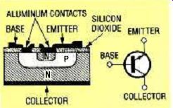
FIG. 1.-NPN BIPOLAR JUNCTION transistor section view (a), and graphic
symbol (b).
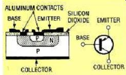
FIG. 2-PNP BIPOLAR JUNCTION transistor section view (a), and graphic
symbol (a).
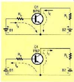
FIG. 3-CURRENT FLOW IN transistors: NPN (a), and PNP (a).
.... requires a negative collector supply with respect to its emitter to operate, and a negative base bias to increase conduction. Fig. 3-b shows conventional current flow in the PNP BJT from the emitter to the collector, as shown in the symbol for the NPN transistor, but opposite to that shown in Fig. 3-a.
Most of the common commodity NPN and PNP BJT's available from electronics distributors and retail stores have been standardized and are made by many different suppliers around the world. Table 1 lists the basic characteristics of two typical general-purpose, small-signal BJT's that are included in the projects discussed in this article: the 2N3904 NPN-type and the 2N3906 PNP-type.
Both are packaged in small, three-pin plastic cylindrical TO-92 packages with flat faces.
Brief definitions for the parameters listed in Table 1 are: Power dissipation is the maximum mean power that the BJT can dissipate without an external heatsink, at normal room temperature, 25 °C. fT is the gain bandwidth product, the frequency at which the common emitter forward current gain is unity.
VcBO is collector-base voltage (emitter open), the maximum voltage that can be impressed across collector and base when the emitter is open.
VcEO is the collector emitter voltage (base open), the maximum voltage that can be impressed across collector and emitter when the base is open.
IC(max) is the maximum mean current that should be allowed to flow through the collector terminal of the BJT. hFE is the DC forward-current gain, the ratio of DC collector current to DC base current for a transistor in a common-emitter configuration The gain bandwidth product, the frequency at which common emitter forward current gain is unity, applies in the following way: If a transistor in a voltage-feedback circuit has a voltage gain of x 100, its bandwidth will be one hundredth of gain-bandwidth value. However if the voltage gain is reduced to x 10, the bandwidth will increase to that value divided by 10.
Transistor characteristics
A knowledge of the static and dynamic characteristics of BJT's will be useful in obtaining the optimum performance from the device. Static characteristics are values obtained when the device is in a test circuit and operated under DC conditions with the measurements made by an ohmmeter.
Figure 4-a shows the static equivalent circuit of an NPN BJT, and Fig. 4-b shows the static equivalent of a PNP BJT.
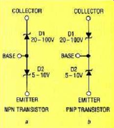
FIG. 4--STATIC EQUIVALENT CIRCUITS for a NPN BJT (a), and a PNP BJT
(b).
Each device can be considered as equivalent to a pair of reverse-biased zener diodes in series between the collector and emitter terminals, with the base terminal connected to the common point between to the two zeners.
Examination of Figs. 1-a and 2-a shows that each BJT is really two diodes: the emitter and base form one PN diode with an emitter-base junction, and the base and collector form a second PN diode with a base-collector junction. When these diodes are properly biased, they reach an avalanche or zener breakdown point.
In most small-signal BJT's, the base-to-emitter junction has a typical zener value of 5 to 10 volts, while the base-to-collector junction has a typical zener value of 20 to 100 volts.
Thus, if the base-to-emitter junction of the BJT is forward biased, it exhibits the characteristics of an ordinary diode.
However, when reverse biased it exhibits the characteristics of a zener diode. The forward-biased junction in a silicon BJT blocks virtually all current until the bias voltage rises to about 600 millivolts.
Beyond that value the current will increase rapidly. When forward biased by a fixed current, the forward voltage of the junction has a temperature coefficient of about -2 millivolts per degree C. When the transistor is configured as an emitter open-circuited, the base-to-collector junction exhibits similar characteristics to those just described except for a greater zener value.
If the transistor is configured with its base open-circuited, the collector–to-emitter path acts like a zener diode in series with an ordinary diode.
Dynamic characteristics
The dynamic characteristics of a BJT can be better understood by examining the typical common-emitter collector characteristics for a small-signal silicon NPN transistor shown in Fig. 5. Direct current collector current Ic is plotted on the Y axis, and DC collector-emitter voltage VcE is plotted along the X axis.
A family of curves for different values of DC base current IB is drawn on Fig. 5. Base current is plotted because the BJT is a current-operated device. As mentioned earlier, the base-emitter junction is forward biased for normal transistor operation.
Base current flows and is a necessary variable for establishing the BJT's operating point.
Observe the following specific points on Fig. 5: When base current (IB) is zero, the transistor conducts barely measurable collector leakage current.
When the collector to emitter voltage exceeds a few hundred millivolts, the collector current value is almost directly proportional to the base current value.
It is only slightly affected by the actual collector voltage value. Thus, the transistor can perform as a constant-current generator by feeding a fixed bias current into the base.
The transistor can also perform as a linear amplifier by super-imposing the input signal on a nominal input bias current. (This will be discussed in more detail later.)
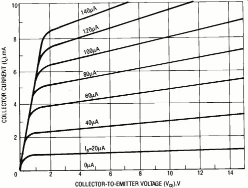
FIG. 5--TYPICAL COLLECTOR CHARACTERISTICS for an NPN bipolar transistor
in a common-emitter configuration.
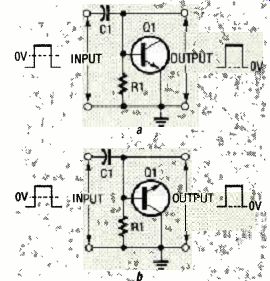
FIG. 6--A CLAMPING DIODE CIRCUIT with an NPN transistor acting as a
diode.
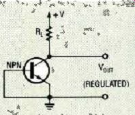
FIG. 7--A TRANSISTOR FUNCTIONING as a zener diode.
Circuit applications
Even a simple small-signal BJT has many applications related to its ability to amplify or switch. Some of the most important and practical circuit designs are described here. With few exceptions, all of the circuits are based on the 2N3904 NPN transistor. (With certain minor component value changes, other NPN transistors can be substituted.) The circuits can also be made with a PNP transistor such as the 2N3906, if the polarities are altered.
Diodes and switches.
It was explained earlier that both the base-emitter and base-collector junctions of a silicon BJT can be considered equivalent to a zener diode. As a result, either of these junctions can perform as a fast-acting rectifier diode or zener diode, depending on the bias polarity.
TABLE 1 RATINGS FOR THE 2N3904 NPN AND 2N3906 PNP TRANSISTORS
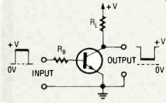
FIG. 8-A TRANSISTOR SWITCH or digital inverter.
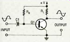
FIG. 9-A COMMON-EMITTER LINEAR amplifier.
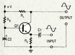
FIG. 10-A COMMON-BASE LINEAR amplifier circuit.
Figure 6 shows two alternative ways to make an NPN BJT perform as a diode in a clamping circuit that converts an AC-coupled rectangular input waveform into a DC square wave. The input AC waveform is symmetrical above and below the zero-voltage reference. However, the output signal retains the input's form and amplitude, but it is clamped to the zero-voltage reference.
If you build this circuit, use the base-collector terminals as the diode as in Fig. 6-b because they provide a larger zener voltage value than the circuit shown in Fig. 6-a.
Figure 7 shows how an NPN BJT can function as a zener diode in a circuit that converts an unregulated supply voltage into a fixed-value regulated output voltage. Typical values range from 5 to 10 volts, depending on the characteristics of the selected transistor. The base-emitter junction is the only one suitable for this application.
Figure 8 shows a BJT functioning as a simple electronic switch or digital inverter. Here the base is driven through resistor RB by a digital input step voltage that has a positive value.
The load resistor RL can be a simple resistor, a tungsten lamp filament, or a relay coil. Connect the load between the collector and the positive supply.
When the input voltage is zero, the transistor switch is cut off. Thus no current flows through the load, and the full supply voltage is available between the collector and emitter terminals. When the input voltage is high, the transistor switch is driven fully on. Maximum current flows in the load, and only a few hundred milli-volts is developed between the collector and emitter terminals.
Thus the output voltage signal is the inverted form of the input signal.
FIG. 11 A DC COMMON-COLLECTOR linear amplifier or voltage follower.
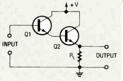
FIG. 12 DARLINGTON DC EMITTER-follower.
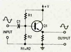
FIG. 13-AN AC COMMON-COLLECTOR amplifier.
Linear amplifiers.
A BJT can function as a linear current or voltage amplifier if a suitable bias current is fed into its base, and the input signal is applied between a suitable pair of terminals. A transistor amplifier can be configured for any of three operating modes: common-emitter (Fig. 9), common-base (Fig. 10), and common-collector (Fig. 11). Each of these modes offers a unique set of characteristics.
In the common-emitter circuit of Fig. 9, load resistor RL is connected between the collector and the positive supply, and a bias current is fed into the base through RB. The value of RB was selected so that the collector takes on a quiescent value of about half the supply voltage (to provide maximum undistorted output signal swings). The input signal in the form of a sine wave is applied between the base and the emitter through C1. The circuit inverts the phase of the input signal, which appears as an output between the collector and emitter.
This circuit is characterized by a medium-value input impedance and a high overall voltage gain.
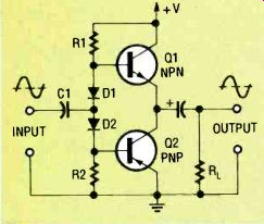
FIG. 14--COMPLEMENTARY OR bilateral AC emitter-follower circuit.
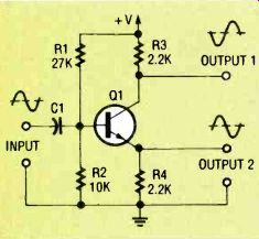
FIG. 15--PHASESPLITTER circuit.
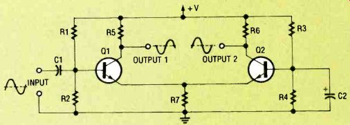
FIG. 16--LONGTAILED PAIR PHASE-splitter.
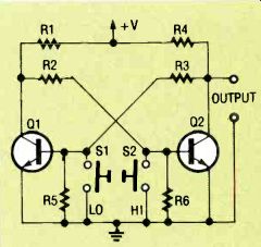
FIG. 17--FLIP-FLOP OR BISTABLE multivibrator with pushbutton triggering.
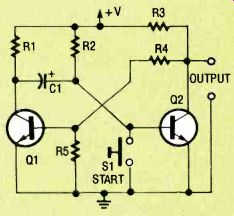
FIG. 18--MONOSTABLE multivibrator with pushbutton triggering.
The input impedance of this amplifier is between 500 and 2000 ohms, and the load impedance equals RL. Voltage gain is the change in collector voltage divided by the change in base voltage (from 100 to about 1000). Current gain is the change in collector current divided by the change in base current or hFE In the common-base linear amplifier circuit of Fig. 10, the base is biased through RB and AC decoupled (or AC grounded) through CB. The input signal is applied between the emitter and base through C1. and the amplified but non-inverted output signal is taken from between the collector and base. This amplifier offers very low input impedance, and output impedance equal to the resistor RL. Voltage gain is from 100 to 1000, but current gain is near-unity.
In the common-collector linear amplifier circuit of Fig. 11, the collector is connected directly to the positive voltage supply, placing it effectively at ground impedance level. The input signal is applied directly between the base and ground (collector), and the non-inverted output signal is taken between the emitter and ground (collector). The input impedance of this amplifier is very high; it is equal to the product of hFE and the load resistance RL. However, output impedance is very low.
The circuit's overall voltage gain is near-unity, and its output voltage is about 600 millivolts less than the input voltage. As a result, this circuit is known as a DC voltage follower or an emitter-follower.
A circuit with very high input impedance can be obtained by replacing the single transistor of the amplifier of Fig. 11 with a pair of transistors connected in a Darlington configuration, as shown in Fig. 12. Here, the emitter current of the input transistor feeds directly into the base of the output transistor with an overall hFE value equal to the product of the values for the individual BJT's.
For example, if each BJT has an hFE of 100, the pair acts like a single transistor with an hFE of 10,000. Darlington BJT's with two transistors on a single chip (considered to be a discrete device) are readily available for power amplification.
The voltage-follower circuit of Fig. 11 can be modified for an alternating current input by biasing the transistor base with a value equal to half the supply voltage and feeding the input signal to the base. Figure 14 shows how this particular circuit is structured.
The emitter-follower circuits of Figs. 12 to 14 can source or feed relatively high currents into an external load through the emitter of the transistor.
However, those circuits cannot sink or absorb high currents that are fed to the emitter from an external voltage source because the emitter is reverse-biased under this condition. As a result, these circuits have only a unilateral output capability.
In many applications (such as audio amplifier output stages), a bilateral output characteristic is essential. A bilateral amplifier has equal sink and source output capabilities. This is obtained with the complementary emitter-follower circuit of Fig. 14. The series-connected NPNPNP transistor pair is biased to give a modest quiescent current through the network consisting or resistors R1 and R2 and diodes D1 and D2. 11-ansistor Q1 can provide large source currents, and Q2 can absorb large sink currents.
Phase-splitters
Transistor linear amplifiers can be used in active filters or oscillators by connecting suitable feedback networks between their inputs and outputs.
Phase splitting is another useful linear amplifier application. It provides a pair of output signals from a single input signal: one is in phase with the input phase. and the other is inverted or 180° out of phase.
Figures 16 and 17 show these alternative circuits.
In the circuit shown in Fig. 15. the BJT is connected as a common-emitter amplifier with nearly 100% negative feedback applied through emitter resistor R4. It has the same value as collector resistor R3. This configuration provides a unity gain inverted waveform at output 1 and a unity-gain non-inverted waveform at output 2.
The phase-splitter circuit shown in Fig. 16 is known as a long-tailed pair because the two BJT's share common-emitter feedback resistor R7. An increasing waveform applied at the base of transistor Q1 causes the voltage to increase across resistor R7, reducing the bias voltage on transistor Q2. This results in the generation of an inverted waveform at the collector of Q1 (at output 1), and an in-phase waveform at the collector of Q2, (at output 2). Multivibrators.
Figures 17 to 20 show BJT's in the four different kinds of multivibrator circuit: bistable, astable, monostable, and Schmitt trigger.
The bistable multivibrator is a simple electronic circuit that has two stable states. It is more often known as the flip flop, but is also called a binary multivibrator, or an Eccles-Jordan circuit. The circuit is switched from one state to the other by a pulse or other external signal. It maintains its state indefinitely unless another input signal is received.
Figure 17 is a simple, manually-triggered, cross-coupled bistable multivibrator. The base bias of each transistor is obtained from the collector of the other transistor. Thus one transistor automatically turns OFF when the other turns ON, and this cycle can be continued indefinitely as long as it is powered.
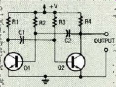
FIG. 19-ASTABLE MULTIVIBRATOR or free-running square-wave
oscillator.
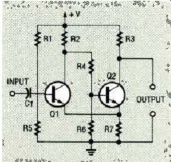
FIG. 20--SCHMITT TRIGGER OR sine to-square wave generator.
The output of the multivibrator in Fig. 17 can be driven low by turning off transistor Q2 with switch S2. The circuit remains "locked" or stable in this state until transistor Q1 is turned off with switch S1. At that time, the output is locked into its high state, and the process is repeated. It can be seen that this action makes it a simple digital memory circuit that holds its state until manually or electronically switched.
Figure 18 is the schematic for a monostable multivibrator or one-shot pulse generator. It has only one stable state. The output of this circuit, a manually triggered version, is normally low, but it switches high for a period determined by the values of capacitor C1 and resistor R2 if transistor Q1 is turned off with switch S1. It then returns to its original state.
The pulse-duration time of the monostable multivibrator can be determined from the equation:
T = 0.69 RC
Where: T is in microseconds, R is in ohms, and C is in micro-farads Monostable multivibrators are used as pulse generators and sweep generators for cathode-ray tubes.
Figure 19 is the schematic for an astable multivibrator or free-running, square-wave oscillator. The transistors are in a common-emitter configuration so that the output of one is fed directly to the input of the other.
Two resistance-capacitor networks, R3 and C1, and R2 and C2, determine the oscillation frequency.
The output of each transistor is 180° out of phase with the input. An oscillating pulse might begin at the base of Q1. It is inverted at the collector of Q1 and is sent to the base of Q2. It is again inverted at the collector of Q2 and therefore returns to the base of Q1 in its original phase. This produces positive feedback, resulting in sustained oscillation.
The astable multivibrator is frequently used as an audio oscillator, but is not usually used in radio-frequency circuits because its output is rich in harmonics.
Figure 20 is a schematic for a Schmitt trigger, a form of bistable multivibrator circuit. It produces rectangular waves, regardless of the input waveform.
The circuit is widely used to convert sine waves to square waves where there is a requirement for a train of pulses with constant amplitude.
The Schmitt trigger circuit remains off until the rising input waveform crosses the preset threshold trigger-voltage level set by the values of resistors R1 and R2. When transistor Q1 is switched ON, transistor Q2 is switched OFF and, the Schmitt trigger's output voltage rises abruptly.
When the input signal falls back below its drop-out level, Q1 switches OFF and Q2 switches ON. The output voltage of the Schmitt trigger drops to zero almost instantly. This cycle of events will then be repeated indefinitely, as long as the input signal is applied.
Also see: Smart Turn Signal