Design PC boards with CAD, and etch them from resist patterns formed by "ironing on" laser-printer toner.
By ALAN NISHIOKA
MAKE SINGLE OR DOUBLE-SIDED PC boards in your own home with this modern method that takes advantage of computer-aided design and the laser printer to form a resist pattern that is transferred directly to the copper-clad circuit board blank. It is an alternative to other methods that have been used by hobbyists who want to make a few prototype boards for their own use.
The alternatives include the time-honored method of applying adhesive pads and fine-line tape masks directly to the circuit board as the etch resist or the use of ultraviolet-sensitive liquid or film resists and photographic methods for transferring the pattern.
The method described here is based on the use of copying machine/laser printer toner powder to form the resist areas to define the circuit board conductive pattern. The pattern is first drawn on the screen of a personal computer with the aid of easy-to-use circuit board design software. The pattern is then printed out on special film in a laser printer. The toner that defines the pattern on the film is then transferred directly to the copper-clad blank by the application of heat from a household laundry iron.
That toner pattern that adheres to the copper becomes the resist pattern. The adhered toner is able to resist the action f the etchant that removes all of the copper cladding from the blank except that which is under the deposited toner.
The process is effective in making simple, single-sided boards, but its merits really show up in the preparation of double-sided boards whose patterns must be accurately registered on both sides. The problem of registering both layers is simple compared with the task of trying to achieve the same results with adhesive tape resist masking or even photographic methods. This article assumes that you will be making double-sided PC boards.
To make boards with this process, you will need an IBM personal computer or compatible for the design phase, and a laser printer to print the pattern with toner on the transfer film (Press-n-Peel from Techniks Inc.). You'll also need, a household laundry iron, a suitable tank for etching the board, and conventional double-sided copper-clad circuit board stock.
Caution: When working with acid you’ll also need a work area and bench or table that is away from the living areas of your house or apartment with adequate safeguards for hazardous materials and ventilation for the removal of toxic fumes.' Although this method can produce complex, double-sided PC boards, it does not include through-hole plating. Solid wire vial or hollow machined pins make any direct electrical connections needed between both sides of the board.
Designing the board.
Personal computer-aided design is an integral part of this toner heat-transfer process because it is the means for delineating the circuit board patterns for both sides of the board. The software used by the author is PC Boards, although other software can be used.
PC Boards has a list price of $99, and is available from the source given in Materials Sources.
PC Boards runs on IBM PC's and compatibles with EGA or VGA capability. It permits you to lay out both sides of a double-sided PC board with the assurance that they will register precisely in later process steps.
Unless you are familiar with the rules that apply to PC board design, it Is advisable to read or review one of the many books available on that subject. Some books cover all aspects including design, acid-etching procedures, and even the selection of drill bits for forming through-holes. Several useful book references are given at the end of this article.
When PC Boards is running on a PC, the bottom layer of the board is displayed in orange while the top layer is shown in yellow (see Fig.1). Objects on both sides of the board (DIP pads, for example) are in blue, has a 0.05-inch grid, and the user can draw DIP's of various sizes and traces of 0.020 or 0.050-inch width.
The program manual covers all of the features of PC Boards.
Read it before doing any design \ work. The program is menu", driven, and you can select the object you want to draw with the keyboard. and use your computer mouse to select the end
\ points of traces and position objects on the board.
`° Place all objects that will have
\drilled holes on 0.10 inch centers (e.g. at 1.20, or 3.70 inches 1;rather than 1.25 or 3.75 inches)
;,So °you can use a small piece of , \ :commercial phenolic circuit
-,'. board with perforations 0.10-
\\\inch on centers as a drill guide.
"À mark located in the lower left
:\ `band corner of the computer ,1*,,, Screen as a reference for the ,computer mouse will help you vith the :layout.
Minimize the number of vias I,'tholes that feed a signal from the top to the bottom layer) because they require drilling.
Where possible, use machined cket pins as vias because must be drilled for them ay. Also, minimize the
. er of traces between DIP pins, particularly those that will 4t'be under the DIP when it is inserted, because they are most kg, likely to cause problems if the r
` °trace patterns on both sides are
\ *improperly registered.
4,
The need for soldering socks!' ets or DIP packaged components from the top surface of " the board also influences component layout and trace placement. If two components are mounted too close together, it will be difficult to get the tip of a soldering pencil between them to make satisfactory soldered joints.
Material purchasing
Copper-clad circuit board blanks are available from many different electronics stores and mail-order distributors. Expect to pay about 10 cents per square inch for double-sided boards.
Regardless of the source and quality of the blanks you buy, be sure to clean them thoroughly so that the toner will stick to the copper and contaminants will not impede the copper-etching process.
Any standard brand household cleaning powder is suitable for cleaning superficial wax, grime, or oil from the boards, and this can be supplemented by scouring the copper surfaces with fine steel wool.
Wear rubber gloves when cleaning the boards to prevent leaving finger prints on the clean copper surfaces. The skin oil in finger prints will corrode the clean copper.
Satisfactory cleaning is indicated by complete surface wetting following a clean tap water rinse cycle. The water should not bead up, an indication of that surface contaminants are still present.
Transfer film
Us 1 *e6tOof Press-n-Peel PCB transfer film from Techntks-t c ( als Sources) .t: .. age to the copper cstadbfa k0(It is priced at $30 for a package of 20 films). Easy-to-foil instructions are provided with each package.
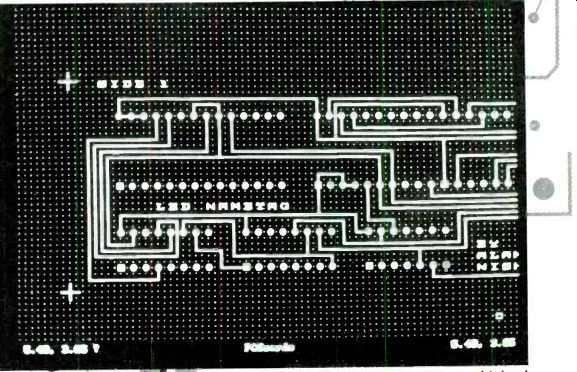
FIG.1--LAYOUT OF ONE PC BOARD PATTERN shown on a computer screen obtained
with circuit board design software. A square reference point and the
coordinate readout are displayed at lower right.
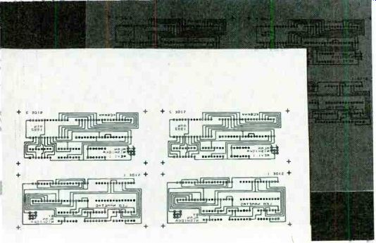
FIG. 2--PC BOARD PATTERN PRINTED ON PAPER with the printed transfer
film shown in the background. Two patterns are printed on the same
film to economize on film. The original patterns have been “flopped" so
the toner can be ironed directly on the copper-clad blank.
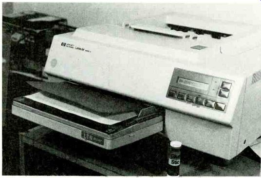
FIG. 3--IRON-ON TRANSFER FILM IS FED INTO THE LASER PRINTER. A backup
sheet of paper can be attached to the leading edge of the film for
support, if necessary.
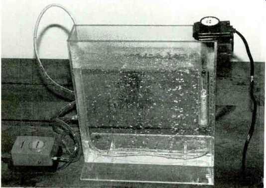
FIG. 4--CIRCUIT-BOARD ETCHING TANK with air bubbler and solution heater
to speed up the etching process and provide more uniform results.
The Press-n-Peel transfer sheet is a plastic film with a blue matte coating. When passed through the laser printer, toner fuses to the blue coating as it does to paper when a document is printed. The transfer sheet is designed so that its plastic backing easily peels away after the toner has been ironed on the copper-clad board. The blue coating also thickens the resist pattern transferred to the board for improved protection against the copper etchant.
Print the layout
The output of the laser printer obtained from the computer with the PC Boards software is a drawing of the circuit board trace pattern with the toner on top as in a normal printing operation. However, to obtain a circuit board pattern that can be ironed directly on the board, the pattern must be inverted.
The author wrote a computer program that will invert the output from the computer running the PC Boards software. This is available as a self-extracting compressed file PCBFLIP.EXE in the Electronics Now BBS (516-293-2283; 2400 or 1200 baud.)
Both top and bottom patterns can be printed on the same transfer film, assuming that the double-sided board measures less than 5 x 8 inches. This approach will economize on the number of transfer sheets needed.
After you have completed the design of both sides of the board, place crosses at two or three locations outside the board patterns to function as registration marks. Locate these marks with respect to the reference mark on each pattern so that when the printouts are placed together, the registration marks will match.
It is recommended that you print out a test sample on quality parchment tracing paper before printing on the actual transfer film. You can then cut apart the two patterns, place their printed sides together and align the paper printouts before you print on the transfer film.
Any mismatches or errors can be corrected at that time without wasting transfer film. The use of a professional (or improvised) light table will make the registration and examination easier.
-----------
MATERIAL SOURCES
Etch Tank System Circuit Specialists
P.O. Box 3047 Scottsdale, AZ 85271
1800-528-1417
Iron-on transfer film DynaArt Designs
3535 Still meadow Lane, Lancaster, CA 93536
(805) 943-4746
PC board design software
PC Boards 2110 14th Avenue
South Birmingham AL 35205
(800) 473 –PCBS
Press-n-Peel iron-on transfer film Techniks Inc.
45 J. Ringo Road
PO Box 463 Ringoes NJ 085551-0463
(908) 788-8249
-----------------
After you are satisfied that the alignment of all circuit board elements is within the expected tolerance levels, print out the transfer film. Feed the transfer film into the single-sheet feeder with the blue matte coating side up. You might find it necessary to attach a paper backing to the transfer film so it will be easier to feed through the laser printer.
Attach the leading edge of the film to the paper backing by applying a narrow stripe of stick adhesive (available at stationery stores) along the leading edge of the underside of the transfer film, leaving the trailing edge free (see Fig. 3).
Iron-on process
Align the transfer sheets for the top and bottom of the board with their printed (toner) sides inward (face to face) on a light table. Staple the two sheets together in three or four places on one edge or tape them among one edge. Slip the cleaned circuit board between the fastened opposing sheets and align it correctly at the edges.
Heat the laundry iron to about 200°F and check that temperature with a mechanical thermometer. If the iron is too hot, the plastic film will melt, distorting the transferred pattern. If it is too cool, the toner will not transfer to the copper surface. You might have to experiment to find the right setting on your iron. However, once you have found it, note that setting for the next time you use this method.
Select a clean, dry, bare wooden board as an ironing surface.
The easiest way to make the transfer is to start with the lower transfer sheet. Place it toner-side up on the ironing surface and put the copper-clad board on top of it. (The attached upper sheet can be folded back out of the way.) Then clamp the board to the film, and apply the iron directly to the top copper-clad surface so the heat will be conducted through the board to the lower surface.
After the film has lightly adhered to the copper, turn it over and iron on the transfer film from the back. Then fold over the upper film, toner side down, and iron it directly on the upper copper-clad surface of the board.
The movement of the iron over the surface helps to loosen the blue coating from the film.
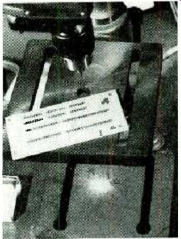
FIG. 5--PERFORATED CIRCUIT BOARD blank serves as a drill jig to obtain
holes spaced in 0.10-inch increments.
Use the tip of the iron to trace over the entire layout on both sides to ensure that all the elements to be transferred have received enough heat and pressure. Take special care with isolated pads and thin traces because they are least likely to transfer properly.
There is no sure way with this method to determine if the complete image has been transferred satisfactorily. The features will appear slightly darker when viewed through the back of the transfer film after the ironing procedure.
Caution: Do not remove the film until the circuit board is cool to the touch.
If, for some reason, small sections of the pattern do not transfer satisfactorily, the gaps can be touched up after the film is removed. The best way to make those minor corrections is to mask them with the black tape intended for the direct-etch process. If larger areas did not transfer, or there are many gaps, the board should be cleaned and the complete process repeated.
Copper etching
A suitable etching tank system is shown in Fig. 4. You can purchase a complete system from a supplier such as Circuit Specialists (see Materials Sources) or you can build your own. Figure 4 shows all the recommended elements for obtaining the best results, but neither the air bubbler nor solution heater are required.
-------------------
AN ALTERNATIVE METHOD
An alternative method for transferring copy machine toner to blank copper-clad circuit boards is offered by DynaArt Designs. It makes special toner-transfer sheets that have a release agent, or "sugar-water" coating on one side of each sheet. A flopped toner image is made on the sugar-water side with a laser printer or copy machine.
The sheet is then placed, toner-side down, on the PC blank, and the toner image is fused to the board with a conventional laundry iron as described in the article. However, instead of peeling off the paper backing, the board is soaked in water until the release agent dissolves and the paper slides off. The manufacturer claims this method assures the complete transfer of all toner.
-----------------------
An article entitled Make Your Own Etching Tank by Tony Lewis appeared in the December 1989 Radio-Electronics on page 45. This article gives complete directions for making a tank from Plexiglas.
The article also includes useful information on the various chemical etchants.
Several different acids available commercially will etch the copper cladding satisfactorily.
However ferric chloride is recommended because it is the most readily available from electronics stores and distributors and it is inexpensive. Unfortunately it is an opaque solution, so it is not possible to observe the etching process through a transparent tank. A 1-liter plastic bottle of the acid costs less than $7.00, but it should be enough to etch more than 500 square inches of copper cladding.
Alternative chemicals are sodium and ammonium persulfate. The per-sulfates are sold in crystal form and have several advantages over ferric chloride in that they will not attack stainless steel, and they are effective when cold. Both give an indication of copper absorption by turning blue as copper dissolves in them--a visual indication that they have lost their etching effectiveness.
Before working with any acid, put on clear safety goggles and wear rubber gloves. Check to be sure there are no pin holes in the gloves for acid to enter. Also make sure that the workplace is well ventilated.
Position the board vertically in the acid so that the etching process occurs uniformly on both sides. The byproducts of the etching process will gravitate to the bottom of the etching tank. The board can be mounted in a carrier, or it can be suspended from nylon monofilament fishing line passed through two drilled holes attached to a bar across the top of the tank.
If you elect to etch with ferric chloride, you will get the best results by heating the solution to about 120 °F and circulating the solution with the bubbler.
Both will reduce the time required to etch away the unwanted copper cladding. It takes about seven minutes to etch an eight-inch square board if the acid is fresh and heated to a temperature of about 100 °F. However, actual etching time will depend on a number of variables: acid concentration, temperature, the degree of agitation, and the surface area to be removed.
Caution: Be sure that the ferric chloride temperature does not reach 180 °F or the toner will dissolve from the board.
Turn off the heater when the etchant temperature has reached at least 100 °F. (You might want to remove the heater to get it out of the way when you are etching the board. It will not cool significantly in the time taken to etch a board.
Remove the board from the etchant periodically, and examine it carefully to see if the etching is progressing uniformly.
Look for any contaminated areas that might be blocking the etching action. When etching is complete, rinse the board thoroughly under running tap water to remove all traces of acid. Caution: ferric chloride attacks most metals and stains porcelain, so use a lot of water in the rinsing process.
Board cleaning
Remove the toner resist manually by scrubbing it with the same combination of household cleanser and fine steel wool that were used to clean the bare copper initially.
Drilling the holes
Use a rigid drill press for drilling the holes in the PC board.
The holes must be accurately positioned and drilled vertically with respect to the PC board. If there is play in the motion of the drill press, the hole might be offset, and there is a risk of breaking a fine drill bit.
A piece of perforated prototyping circuit board with holes drilled 0.10 inch-on-centers works well as a drill jig. Circle the holes in the perforated board that are to be used as a drill guide with a colored marking pen so they can located quickly in a logical sequence while drilling.
Clamp the perforated board jig to the circuit board with double-sided adhesive tape to keep the two pieces from shifting with respect to each other.
When drilling the board through the jig, hold the combination so that the drill bit can self-center in the pilot hole. Be sure to press down firmly on the work when the drill bit is withdrawn to prevent it from being caught and breaking off.
Periodically check to be sure that all drilled holes are centered in the pads on both sides.
You might have to offset the drill jig slightly to average out any alignment error on both sides.
Minor hole runout in a series of aligned holes (such as required for mounting SIP's and DIP's) can be tolerated; the error build-up should not be enough to hinder device pin insertion.
Through-hole conduction
Complete all vias first. These are conductors inserted through the board and soldered to pads on both sides. Insert a length of bare copper wire with the same diameter as the drill bit in the via hole, and solder it to the pads on both sides of the board. Then trim the wire close to the board surface on both sides with a wire cutter.
Because these boards don't have plated through holes, low-profile sockets with hollow machined pins are needed if you want to solder component pins to traces on both top and bottom surfaces of the board. Alternatively, you can use individual machined socket pins.
The machined pins call for slightly larger drilled holes, but they can be soldered to the board in the same way as the vias. Try to avoid getting any solder inside the hollow pins while soldering them to both top and bottom pads.
References
Electronic Prototype Construction. by Stephen D. Kasten, 1983, Howard W. Sams & Co.
Printed Circuits Handbook by Clyde F Coombs, Jr..1988 McGraw-Hill, Inc.
Also see: THE SPECTRUM ANALYZER