Proper heat management ensures that components have a long and healthy life.
by STEPHEN J. BIGELOW

WHENEVER CURRENT FLOWS through an electronic component, that component dissipates power. The power that the part dissipates depends on both the current flowing through the part and the voltage across it, and can be expressed by the relationship P= IV. Heat is an unavoidable byproduct of power dissipation.
For many circuits and components, heat generation is negligible or so small that the component can easily shed its heat buildup directly into the air. Some components, however, can not give up heat fast enough, and excessive heat buildup occurs. When that happens, the device can be permanently damaged. Thermal management techniques, such as the two common heatsink arrangements shown in Fig. 1, must be used to improve the component's heat dissipation.
This article will explain the concepts of heat management and show you how to use manufacturers' specifications to optimize component operation.
You can use these techniques with most semiconductor devices.
Thermal circuits A thermal circuit is a graphic representation of thermal energy's path from its source to ambient air. In many ways, thermal circuits are analogous to electronic circuits as shown in Fig. 2.
Notice that there is resistance to the flow of heat between the heat source and the air. Such thermal resistance is generally defined as the difference in temperature across two points, divided by the power being dissipated between those two points. Thermal resistance is symbolized by the Greek letter theta (A) and is measured in degrees Celsius per watt ( °C/W). As a rule, thermal resistance should be as small as possible between the power-dissipating semiconductor junction(s) and the ambient air. Low thermal resistance between junctions ensures minimum junction temperature.
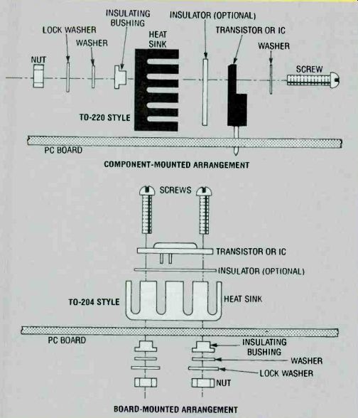
FIG.1--THERMAL MANAGEMENT TECHNIQUES, such as these two common heatsink
arrangements, must be used to improve a component's heat dissipation.
Heat sources
Heat is generated by a semiconductor device when it dissipates power. A diode dissipates power at its anode-cathode junction. Junction power can be defined as the current through the junction multiplied by the voltage drop across the junction (typically 0.6 volt DC for a silicon diode). Power dissipated by a transistor is the voltage drop between the collector and emitter multiplied by the collector current. The power dissipated by an integrated circuit is the total power dissipated by all of the integrated circuit's transistors.
Thermal resistance
The heat generated in a semiconductor junction does not dissipate directly to the ambient air. Instead, a number of thermal resistance factors must be taken into account. The use of an external heatsink typically involves three major thermal resistances: (1) between the semiconductor junction and the device's case, (2) between the case and the attached heatsink, and (3) between the heatsink and the ambient air. Additional thermal resistance might be encountered if an electrical insulator is included between the case and heatsink.
For components that do not use an external heatsink, two thermal resistances must be considered: (1) between the semiconductor junction and the case, and (2) between the case and the ambient air. The total thermal resistance of a semiconductor arrangement can be summarized as shown in Table 1.
The junction-case resistance (Hjc) represents the flow of heat from a device's junction(s) to its outer case. The value of 0 J is specified by the manufacturer in his data sheet. A smaller number represents better heat flow. Junction-case thermal resistance is dependent on a number of physical characteristics. These include the size and shape of the semiconductor die and its mount, the quality of the die-to-mount bond, and the thermal conductivity of the die, mount, bond, and any interconnecting wires.
Although you have no control over HJc, you can select a particular case style that minimizes the thermal resistance.
Figure 3 shows what the different case styles look like. For example, a transistor in a TO-220 case has better (lower)
HJc than a similar device in a TO-92 case. Table 2 shows a selection of typical 0 J values for a variety of case styles. If you do not have access to manufacturer's data, Table 2 can provide a good approximation.
The use of a heatsink can have a tremendous impact on a component's operating temperature. For some devices, a good heatsink can mean the difference between a successful project and a failure. The goal of a heatsink is to move as much heat as possible away from the device's junction, and that's accomplished through the choice of heatsink, mounting arrangement. and mounting materials.
Thermal resistance at the case-sink barrier (Hcs) is a function of many factors: (1) the cross-sectional contact area between the case and sink, (2) the mating surface finish and flatness, (3) the contact force (or pressure) applied between mating surfaces, and (4) the thermal resistance of any electrical insulating material needed between the case and sink. You have a lot of options in determining each of these factors.
---------------
FIG. 2--A THERMAL CIRCUIT is a graphic representation of thermal energy's
path from its source to ambient air. Thermal resistance is defined
as the difference in temperature across two points, divided by the power
being dissipated between those two points. Thermal resistance should always
be as small as possible.
HEAT SOURCE EIcS E WITH HEATSINK esc ecA 1 MA WITHOUT HEATSINK 1
0=4T/P
0= THERMAL RESISTANCE ( °C/W)
4T= TEMPERATURE DIFFERENTIAL ( °C)
P =POWER ( WATTS) J= JUNCTION C =CASE S =SINK
A= AMBIENT
--------------------
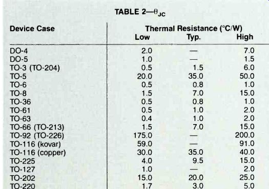
TABLE 1 THERMAL RESISTANCE SUMMARY
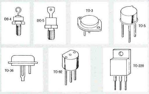
FIG. 3 DIFFERENT COMPONENT PACKAGES vary in their ability to dissipate
excess heat. Here are some of the more popular styles.

TABLE 2-6 jc
-------------
There are some general rules to follow in determining the characteristics of your heat-sink. It is important that the surface areas of the component case and heatsink be as flat and smooth as possible. Thermal joint compound conducts heat very well, and can be applied between the case and heatsink to help overcome any surface irregularities. Large contact areas between the case and heat sink are helpful because larger mating areas will improve heat conduction. Wherever screws are used to attach a heatsink to a case, be sure they are securely fastened to flatten any concave or convex mating surfaces and achieve good contact pressure.
The actual Ocs for a heatsink is specified for each particular model in a manufacturer's catalog, but Table 3 provides a typical range of thermal resistance values for several major classes of heatsinks.
When electrical insulators are used to isolate a case from a heatsink, heat must still be transferred as effectively as possible. Unfortunately, most electrical insulators will add some thermal resistance (OINS) to the case-sink interface. Table 4 shows a selection of various electrical insulators. If your mounting arrangement requires the use of an insulator, add GINS to Ocs from table 3.
Notice that an insulator's thermal resistance depends on the type of semiconductor package being insulated.
The ability of any heatsink to dissipate heat depends on a complex combination of conduction, convection, and radiation. With all three of these factors working together, it's difficult to calculate the specific thermal resistance of any one particular heatsink. Fortunately, manufacturers typically list the sink-ambient thermal resistance (0SA) of their various models. However, if you don't have manufacturer's information, Table 5 lists values that permit good approximations.
As a general rule, larger, thicker heatsinks with more substantial surface area have a lower 0SA than small, thin heat-sinks. Also notice that Table 5 shows 0SA for both still and moving air; when air is in motion, the effect of convective cooling is enhanced, and more heat is carried away--in other words 0SA is much lower.
Every kind of semiconductor case differs in its ability to dissipate heat directly into the air, but no case does this as well as heatsinks. The major reason is that air does not support conduction or radiation very well-most heat is carried into the air by convection. When a heatsink is used, heat from a device's case is carried into the heatsink directly by conduction. Without a heatsink, however, a device must rely solely on convection to take the heat away. As a result, the thermal resistance from a case to the ambient air (0cA) is usually quite high, and heavily dependent on the size and shape of the particular case.
Generally speaking, larger metal cases (such as a TO-3) dissipate heat better than small, low profile plastic cases (such as a TO-92). Manufacturer's specifications for a device might list OCA along with OJc, but don't count on it.
Table 6 shows some common values of OCA for a variety of case styles. Note that small cases can have large thermal resistance values that can seriously limit the device's ability to handle power.
Total resistance
Here is a practical example of how to calculate total thermal resistance from the junction to ambient air (0JA) for a TO-3 case transistor using a large metal heatsink in still air with no electrical insulator. Remember that a TO-3 is a metal case-mounted semiconductor. From Table 2 you know that 0JA is the sum of 0Jc, OAS, and OSA. Junction-case thermal resistance can be found on a manufacturer's data sheet, or approximated from Table 2 (typically 1.5 °C/W). Case-sink thermal resistance for a metal cased, case-mounted semiconductor can be approximated from Table 3 (0.5 °C/W). Table 4 is not needed because we're not using an insulator.
The sink ambient thermal resistance for a large metal heat-sink operating in still air can be found in manufacturer's data for the heatsink, or approximated from Table 5 (5.0 °C/W). These characteristics yield a total thermal resistance of 1.5 + 0.5 + 5.0, or a 0 J of 7 °C/W.
As a second example, under the same conditions as the previous example, you can determine the total thermal resistance when no heatsink is used.
From Table 1 you know that the value of 0JA--with no heatsink--is the sum of 0 J and OCA. Junction-case thermal resistance remains the same as in the previous example (1.5 °C/W), but the value of case-ambient thermal resistance is now obtained from Table 6 (30 °C/W). This yields a new OJA of 1.5 + 30.0, or 31.5 °C/W-a very significant increase.
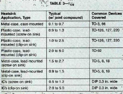
TABLE 3-Hcs
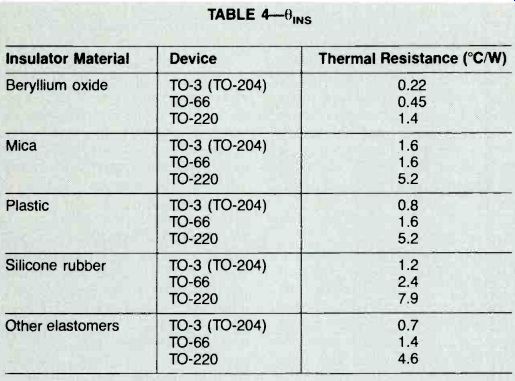
TABLE 4-HINs

TABLE 5-0SA
Safe operation
It is often desirable to estimate the junction temperature of a semiconductor to determine if it will work within its safe operating range. This technique can be handy for estimating heatsink performance.
The maximum junction temperature (T1) of a semiconductor device is normally specified on the manufacturer's data sheet. However, maximum junction temperature will not exceed 100 °C for a germanium device, or 200 °C for a silicon device. If Tj is exceeded, even for a brief period of time, the device will probably be destroyed.
Junction temperature can be calculated from the relationship shown in Table 7. Power dissipation (Pd), total thermal resistance (0 JAL and ambient temperature must be known.
For most practical purposes, ambient temperature can be considered to be room temperature, or 25 °C. Steady-state power dissipation in a semiconductor device can easily be calculated from Ohm's Law as the voltage drop across a device multiplied by the current flowing through the device. Total thermal resistance can now be approximated from the contents of tables 2 through 6.
By comparing the specified maximum junction temperature with the value calculated from present operating conditions, you can estimate a device's operating temperature. If your calculations indicate a temperature well below the maximum Ti, the device will probably run safely. If, however, your calculations indicate a temperature close to or higher than the maximum T, the device will be in a region where it can destroy itself. Power dissipation, thermal resistance, or ambient temperature must be reduced to reduce the junction temperature to a safe level. Although ambient temperature can be adjusted, it is usually impractical to do so.
Here are some basic examples. According to a manufacturer's data sheet, the maximum junction temperature for a TO-220 transistor is 150 °C. Determine if the transistor is operating safely if it's dissipating 2 watts of power in still air. It has a medium-sized, bolt-on heatsink and a beryllium oxide insulator attached.
Because power dissipation (2 watts) and ambient temperature (assumed 20 °C) are known, it is necessary to estimate the value of total thermal resistance. Total thermal resistance (0JA) is the sum of O jo, °CS' OINS, and OsA. From Tables 2 through 5 you know that the junction-case thermal resistance is 7.0 °C/W ( Table 2), case-sink thermal resistance for a plastic-cased, lead-mounted semiconductor is 1.1 °C/W (Table 3), insulator thermal resistance is 1.4 °C/W (Table 4), and the thermal resistance for the associated heatsink is 17.0 °C/W (Table 5). Therefore, the total thermal resistance is 26.5 °C /W. Next, the junction temperature can be calculated from the relationship given in Table 7. A device consuming 2.0 watts of power at 26.5 °C /W yields a temperature rise of 53.0 °C (2.0 °C x 26.5 °C) above ambient temperature. Adding the ambient temperature yields a junction temperature of 78 °C (53.0 °C + 25.0 °C). Since the calculated value of T1 is far below the specified maximum of 150 °C, the TO-220 transistor should be operating safely within its limits.
As another example, remove the heatsink and insulator from the transistor in the previous example and determine whether or not the transistor will still be operating safely.
Keep in mind that power dissipation (2 watts), maximum specified T1 (150 °C), and ambient temperature (25 °C) remain the same-the factor that changes substantially is the total thermal resistance. Without a heatsink, OJA can be estimated as the sum of junction-case and case-ambient thermal resistance. Since the transistor remains unchanged, the junction-case thermal resistance remains unchanged at 7.0 °C/W (Table 2). The case-ambient thermal resistance for a TO-220 transistor can be estimated from Table 6 (60 °C/W). That yields a total thermal resistance of 67.0 °C /W (7.0 °C + 60.0 °C). Using the formula of Table 7, the new junction temperature rise would be 134.0 °C (2.0 X 67.0) above ambient. The junction temperature would then be 159 °C (134.0 °C + 25.0 °C). Our calculations indicate that, without a heatsink, power dissipation will result in a destructive temperature at the device junction of 159 °C which exceeds the specified limit of 150 °C. Although the device might work for some time at that level, thermal breakdown is almost inevitable. To prevent damage to the device, it is necessary to replace the heatsink or reduce power dissipation.
Maximum power
Instead of calculating a junction temperature to determine whether or not a semiconductor is operating safely, you can use the formula in Table 7 to calculate the maximum allowable power dissipation for a desired set of operating conditions.
This approach allows you to select a desirable junction temperature (below the specified maximum T) and then find the maximum power dissipation that will not exceed the desired junction temperature.
The first step in calculating maximum power is to determine the maximum junction temperature for the semiconductor device that you are using. A T1 rating is usually listed on a manufacturer's data sheet. Power dissipation can then be calculated from the relationship given in Table 8. Ambient temperature is still considered to be 25 °C. The total thermal resistance (0JA) can be estimated from Tables 2 through 6.
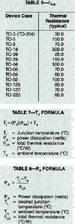
TABLE 6-HcA
TABLE 7-I, FORMULA
TABLE 8-Pd FORMULA
It is usually undesirable to operate the device at or around its maximum Ti. Use a smaller value in your calculations to allow a safety margin. For example, a 20% safety margin for a maximum Tj of 160 °C would be 128 °C (160-(160 x 0.2)). A 50% safety margin would be 80 °C (160 °C-(160 °C X 0.5 °C) ). Incorporating a safety margin into the calculations ensures that the device will be running within safe limits at all times.
Look at another example. A transistor in a TO-66 case has a maximum T of 180 °C. The transistor has a metal case and a case-mounted, medium-sized heatsink with a mica insulator.
You want a 40% safety margin for the junction temperature, so you can estimate the maximum allowable-power dissipation for the device in still air.
First estimate the total thermal resistance of the arrangement from Tables 2 through 5.
Total thermal resistance (0JA) is the sum of 0 J (7 °C/W from Table 2), 8cs (0.5 °C/W from Table 3), °INS (1 °C/W from Table 4), and 0SA (13 °C/W from Table 5). That yields a sum of 21.5 °C /W total thermal resistance.
The desired junction temperature is the maximum specified Tj minus a 40% safety margin.
That works out to a desired junction temperature of 108 °C (180 °C-(180 °C x 0.40 °C) ). Finally, use the formula in Table 8 to determine the maximum allowable power dissipation for the device. With a temperature difference of 83.0 °C (108 °C-25 °C) and a thermal resistance of 21.5 °C /W, the maximum allowable power dissipation (Pd) for the device is 3.9 watts (83/21.5). With the same transistor and desired junction temperature from the previous example, let's estimate the maximum allowable power dissipation for the device in still air with a large heatsink and no insulator. A large heatsink and no insulator will substantially reduce the total thermal resistance of the arrangement. Tbtal thermal resistance is now the sum of 0 j (7 °C/W from Table 2) 0cs (0.5 °C/ W from Table 3), and 0SA (5.0 °C/ W from Table 4); 0JA is now 12.5 °C /W, a large decrease from the last example. The desired junction temperature stays the same at 108 °C, so the temperature difference between junction and ambient remains constant at 83 °C. Finally, use Table 8 to find the value of maximum allowable power dissipation. The value of Pd is 6.6 watts (83/12.5). As you can see, just using a larger heatsink and removing the insulator can virtually double the allowable power of the device, and still keep the device's junction temperature 40% below its maximum rating.
After allowable power is calculated, you can work backwards with Ohm's law to gauge the appropriate voltage and current for operating the transistor. In some instances, minor circuit changes might be necessary to limit voltage or current.
Power derating
The power that a device can dissipate is closely related to its junction temperature. Once a certain junction temperature is reached, the maximum allowable power drops off in a linear fashion as junction temperature continues to increase-and the junction temperature can only climb to Tj before permanent device damage occurs.
Most manufacturers will show a detailed plot of power dissipation vs. junction temperature with their specifications.
This type of plot, known as a power derating curve, is illustrated in Fig. 4. The derating factor (DF) is essentially the slope of the line that represents how quickly allowable power will drop off as temperature increases. Expressed another way, DF is the inverse of the junction-case thermal resistance WO Jo). Remember that power derating is for the device alone-it does not consider the effects of an attached heatsink.
The maximum safe power rating anywhere within the linear region of the derating curve is given by the formula in Table 9.
To determine power at any linear point, calculate the derating factor from either the line's slope, or from the inverse of 0 jc.
Then use the relationship in Table 9. Look at the following example.
Using the power derating curve of Fig. 3, find the maximum allowable power dissipation for the device at a junction temperature of 130 °C. First it's necessary to calculate the power derating factor (DF) of the curve. Figure 3 shows that DF is equal to the maximum allowable power (10 watts), divided by the difference between the maximum junction temperature (180 °C) and the temperature where derating begins (100 °C). The DF is then 0.125 (10 /(180 °C-100.0 °C)). Then, use the formula in Table 9 to find allowable power at the desired temperature point (130 °C). Allowable power (Px) is equal to 6.25 watts (10((130-100) X 0.125))). Notice that when its junction temperature is below 100 °C, the device can dissipate up to its maximum power of 10 watts.
Above a junction temperature of 100 °C, the amount of power that the device can dissipate will decrease at a rate of 0.125 watts for every 1 °C of junction temperature increase. If a heat-sink is used, junction temperature will be reduced and the device can dissipate increased power.
Conclusion Whether you are evaluating the design of a project, or designing a project of your own, heat management plays an important role in your work. When a component must handle any sizable amount of power, the inevitable byproduct-heat-can destroy or damage part's operation and overall reliability. The objective of heat management is to carry enough heat away from the power-dissipating junctions of a device to allow reliable, long-term operation. The ample use of heatsinks is an effective and economical means of removing heat from a device. But there are a variety of important thermal resistance factors that must be considered to ensure that a heatsink arrangement will function as desired.

TABLE 9--MAXIMUM POWER
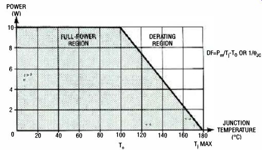
FIG. 4--A POWER DERATING CURVE shows how allowable power drops off as temperature
increases.
------------------
Also see: HARDWARE HACKER