by MARK DANIELS
A 250 W to 600 W design with pulse width modulation for voltage control and an uninterruptable supply add-on. It can also be built for 50Hz or 60Hz operation.
PORTABLE mains power usually means large, noisy gasoline or diesel generators which tend to be expensive, in terms of both capital and running costs, especially for smaller loads. The Battery to Mains Inverter published in the March 1991 issue of Everyday Electronics was developed to meet the requirement for a silent and portable source of mains voltage electricity. Unfortunately one or two of the components have recently become impossible to source, so a complete re-design has been undertaken.
IMPROVEMENTS
Looking back at the spec. sheet for the original design revealed several areas where improvement could be made. The power rating is one such area, but will obviously require the primary power source to be capable of sustaining a somewhat heavier current drain.
An investigation into the properties of car batteries and the type of loads likely to be used with an inverter reveals that it is possible, with care, to increase the inverter rating considerably. Specialist batteries with a deep cyclic discharge rating, such as caravan or traction batteries, are obviously ideal for this application, but tend to be quite expensive. Standard vehicle batteries are cheaper and, when loading is likely to be intermittent or of short duration, may be equally suitable. An 069 battery, as fitted to the author's Land Rover, is typical of the unit supplied with many modern cars. Its capacity of 63 ampere-hour at the twenty hour rate enables it to supply 31 5 amps for twenty hours, delivering a total of 0.75kW hr of energy into the load.
Unfortunately, the energy available from an accumulator falls dramatically as the load current increases. Even so, we can expect this particular example, when fully charged, to be capable of sustaining a continuous current drain of 25 amps for 100 minutes, i.e. it will still supply as much as 0.5kW hr.
A 250 Watt continuously rated inverter with a short term overload capacity of 400 Watts will run most portable power tools from a fully charged car battery for a useful length of time. A peak inverter efficiency of about 85 percent ensures that the majority of the input energy is available to the load, with the battery supplying 25 to 40 amps to the inverter. As it is rarely necessary to run an electric drill for more than a few minutes at a time this level of current consumption is quite acceptable.
The 250 Watt continuous rating of this unit will enable it to power many small domestic appliances, including personal computers which may be shut down in an orderly manner when the mains fails.
A U.P.S. (Uninterruptable Power Supply) add-on to be described in Part 3 takes care of the battery charging and the change over from mains to battery when the power fails.
The inverter may be built as either a 50Hz or a 60Hz version and, in conjunction with the U.P.S add-on, may perform as a frequency changer to allow equipment of American origin to operate satisfactorily on British mains.
--------------
Specifications
For 250W Inverter
Power Rating, Continuous Power Rating, Continuous with Fan Instantaneous Power Rating Input Voltage Range Maximum Input Current Output Frequency Options Frequency Stability Output Voltage Peak Efficiency Weight 250 Watts 300 Watts 400 Watts 10.5 to 13.8 Volts 40 Amps Peak 50Hz or 60Hz
< 50ppm 240 Volts, regulated
>85 percent
< 5kg
Specification for 600W Option as above, with the following exceptions)
Power Rating 600 Watts Instantaneous Power Rating 1000 Watts Maximum Input Current 100 Amps Weight < 10kg
-------------------
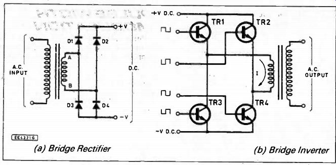
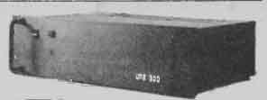
Fig. 1. The bridge configuration.
Fig. 2. The half-bridge configuration.
INVERTER CONFIGURATIONS
There are many ways of providing ac. to a transformer from a d.c. power source, but for low, fixed frequencies only three of these are in general use: the Bridge, Half Bridge and Bi-Phase (or Push-Pull). All three of these configurations have rectifier counterparts and a series of useful analogies may be made, which will be helpful in gaining an understanding of the process of inversion.
BRIDGE CONFIGURATION
The bridge inverter is perhaps the easiest to understand, not being complicated by the need for a centre-tapped transformer or capacitors. Fig. lb shows the basic circuit for the bridge configuration, with a bridge rectifier shown in Fig. la for comparison purposes.
In the bridge rectifier the diodes allow current to flow only when they are for ward biased. This will occur for D1 and D4 when point A is more positive than point B, current will then flow through DI, through the load and return to the supply via D4. When the polarity of the a.c. sup ply reverses and point B becomes more positive than point A the current will flow through D2, through the load, in the same direction as before and return to the supply via D3. The load will experience a unidirectional flow of current, equivalent to d.c.
In the inverter an electronic timebase controls the transistors which are turned on in pairs, TR1 with TR4 and TR2 with TR3, thus permitting the current to flow alternately in one direction and then the opposite through the transformer primary winding. If TR1 and TR4 are turned on (with TR2 and TR3 off) current will flow from the positive supply rail, through TRI, through the primary winding of the trans former in the direction indicated by the arrow and through TR4 to return to the supply via the negative rail. With TR2 and TR3 turned on (TR1 and TR4 will be off) the current flow in the winding will be in the opposite direction to that indicated.
The output voltage from the bridge rectifier and the bridge inverter is equal to the supply voltage, less semi-conductor losses, in each case. Neither circuit requires a transformer in order to function, though both are commonly used in conjunction with one.
HALF-BRIDGE CONFIGURATION
The half-bridge rectifier is normally referred to as a voltage doubler circuit, since that is precisely what it does. Fig. 2 shows the circuits for the rectifier and the inverter.
Capacitors are substituted for two of the diodes in the bridge rectifier resulting in the half-bridge. Now when current flows each of the capacitors will charge up to the peak a.c. voltage on opposite half cycles and, since they are connected in series, their voltages are arithmetically additive, giving a d.c. output voltage equivalent to double the peak supply voltage.
In the half-bridge inverter the two transistors are switched alternately driving point A of the transformer primary winding first negative and then positive with respect to point B which is held at half the d.c. supply voltage by the two capacitors. It is only possible for point B to remain at this voltage if a.c. is flowing in the winding.
Any d.c. component will cause the voltage at B to shift, reducing the value of the a.c. presented to the load. This automatically compensates for asymmetry in the a.c. waveform supplied to the transformer.
The half-bridge inverter has an a.c. output voltage of only half the d.c. supply voltage.
THE BI-PHASE COAIFIGURATION
All of the above circuits have made use of a single, untapped winding, achieving apparent simplicity. Adding a centre-tap to the winding would appear to complicate matters, but in practice it simplifies things considerably by reducing the component count and, in the case of the inverter, can also simplify the timebase design. The respective circuits for the bi-phase rectifier and inverter are shown in Fig. 3a and 3b.
The operation of the rectifier is very simple; when point A is more negative than the centre-tap (C.T.), current will flow from C.T. through the load and return to the secondary winding via Dl. On alternate half-cycles of the sine wave A will become positive with respect to C.T. and current flow will be blocked by D1 which is now reverse biased. C.T., however, will be more positive than B and current will flow through the load and D2 in the correct direction. The resultant current flowing in the secondary winding will be an alternating one.
As in the previous two cases the reverse process may be applied to achieve inversion. The two switching transistors are supplied with square wave signals having a phase difference of 180 degrees thus producing a resultant alternating current in the secondary winding.
The voltage across the entire winding is twice the d.c. voltage for this configuration, thus enabling transformers of sensible electrical proportions to be used with a relatively low d.c. supply.
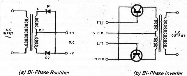
Fig. 3. The bi-phase configuration. (a) Bi-Phase Rectifier (b) Bi-Phase
Inverter
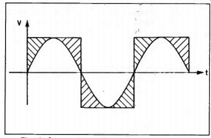
Fig. 4. Comparison of square and sine waves.
INVERSION
It is interesting to note that these configurations bear more than a little resemblance to three of the most familiar rectifier arrangements. This is hardly coincidence, since inversion is merely the reverse of rectification and similarly involves coupling of the d.c. circuit to the a.c. circuit through switches which are opened and closed at the appropriate times. In rectification the switches are, of course, diodes which are forced to switch at the correct time by the pre-existence of an a.c. waveform.
With inversion the pre-existence of an a.c. waveform cannot be taken for granted, as the primary source of power is normally d.c., so a method of forced switching has to be employed. This implies a necessity for controllable semiconductor switches in place of the rectifiers, e.g. thyristors or transistors. The standard thyristor (more correctly known as a "reverse blocking tetrode thyristor") is usually restricted to high voltage, high current applications on the grounds of cost and circuit complexity.
Complicated forced commutation methods are essential for proper circuit function and, unless correctly set up, can lead to premature device failure. Special types of thyristor, such as the gate turn off (G.T.O.) device alleviate the commutation problem, but tend to be even more expensive than standard devices and are generally only available with relatively low current ratings.
POWER TRANSISTORS
The hi-polar power transistor requires few of the circuit complications of the thyristor and is generally much simpler to use. Modern devices are available with current ratings comparable to mid-range thyristors (500 to 600 amps), and have switching speeds a factor of ten or more higher. The transistor also has a considerably lower forward volt drop when conducting (typically 0.2V when saturated, compared with more than IV for a thyristor), which is a considerable advantage, particularly in low input voltage applications such as this. It offers greatly improved efficiency and reduced device heating, thus enabling smaller heatsinks to be employed.
The transistor, however, has no reverse blocking capabilities and external protection must be employed to prevent device breakdown, normally with an inexpensive silicon rectifier. The power devices also re quire a larger control current compared to the thyristor, requiring multiple stage amplification to reduce this to a suitable level. Even taking this into consideration use of transistors will usually work out considerably cheaper than an equivalent thyristor in this type of application.
Only the half-bridge has automatic symmetry correction, although this may also be applied to the bridge type by the addition of a capacitor in series with the primary winding. This is not very often seen as it requires the use of a large non-polarised component to carry the high a.c. current.
SQUARE WAVE VERSUS SINE
The normal mains electricity supply is an alternating one of sinusoidal waveform, which is characteristic of electricity generated in a rotating machine. The sine wave has the advantage that it is pure and free from harmonics, making it ideal for circuits containing inductive or capacitive reactance. I also simplifies many of the calculations which we take for granted, such as peak to r.m.s. conversion, although suitable equations may also be developed for other wave shapes as will be demonstrated later.
Unfortunately, the sine wave does have some serious disadvantages compared to another type of waveform, the square wave, when developed by means of analogue electronics.
Most importantly an ideal square wave has zero rise and fall times and a peak value equal to the supply voltage, thus no energy is lost in converting d.c. into this form of a.c.
With a sine wave the voltage varies continuously and smoothly in accordance with a simple mathematical relationship. This requires a considerable amount of time for the transition from one peak to the other and causes the transistor to spend long periods of time in a state where it is dissipating a lot of power.
It may be seen from the drawing of Fig. 4 just how much of the energy is lost and why. The sine wave is totally enclosed by the square wave as is an additional area indicated on the drawing by the shaded area which represents the power lost in analogue methods of sine wave production. Simple graphical measurement techniques or analytical calculus methods show the area enclosed by the sine wave to be 70.7 percent of that enclosed by a symmetrical square wave of similar amplitude.
REGULATION
The output voltage of an inverter is load and input voltage dependent, with the transformer regulation playing an important part in the load regulation. In a fixed voltage (unregulated) inverter it is necessary for the supply voltage to be absolutely stable and the core and winding losses of the transformer to be practically non existent for the output voltage to remain constant under all conditions of loading.
Unfortunately, in real life these ideals are unlikely to be met and external regulation will generally be employed. This normally entails designing the transformer to provide a higher off-load output voltage than is required and controlling the input to the transformer in a manner which gives the desired output voltage under all normal load conditions.
The most obvious method is linear regulation, which may be employed to good effect in small inverters, the excess voltage being dropped across a series pass transistor and dissipated as heat. The basic principle is very simple, but in practice may not be quite as straight-forward as this, particularly with larger designs.
There are alternatives such as inductive control methods using chokes or magnetic amplifiers, but these require specialized wound components which tend to be expensive or difficult to produce at home and are generally unavailable through the usual sources.
Control via the switching transistors eliminates the need for extra components in the high current or high voltage sections of the circuit, and can be achieved quite simply by varying the duty cycle of the square wave.
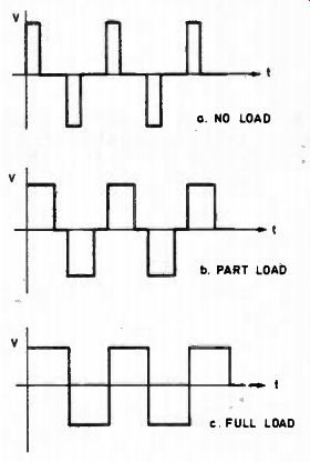
Fig. 5 Pulse width modulation wave forms.
PULSE WIDTH MODULATION
Pulse-width modulation (p.w.m.) is commonly used in switched-mode power supplies of the type fitted to virtually all personal computers. Although considerably more complex than linear regulation it offers several significant and important advantages, not least of which is the greatly improved efficiency. With less heat to dissipate smaller (and cheaper) heatsinks may be used, leading to a more compact and cooler running unit, which will ultimately be more reliable.
Pulse width modulation introduces into the standard square waveform a "dead time" when neither switching transistor is permitted to conduct. The pulse width may be adjusted to alter the output voltage of the inverter, or, more usually, to keep the voltage constant as the load current or supply voltage varies. Fig. 5 shows some examples of typical output waveforms for a p.w.m. inverter, under varying conditions of load current and input voltage.
The dead-time gives the p.w.m. inverter its characteristic 3-level output waveform.
Under no-load conditions the peak voltage may be quite high (Fig. 5a) and to compensate for this the pulse width will be fairly narrow. As the load is increased the output voltage falls and the pulse width is increased to maintain the r.m.s. voltage as in Fig. 5b. Full load conditions demand maximum power and consequently the pulse width must be increased to its maximum.
The expected (and desired, from the load's point of view) waveform to satisfy this condition would be one with zero dead-time as in Fig. Sc. Unfortunately, this does little for the life expectancy of the switching transistors which need a finite length of time in which to carry out the switching operation. The transformer primary winding is largely inductive and by its very nature will oppose any change in current. The combination of these two factors will result in large currents and voltages being generated which will ultimately destroy the transistors. In small inverters (up to 100 Watts) this effect is minimal and may usually be ignored.
To overcome the above problem the maximum output pulse width is normally limited to around 90 or 95 percent of the half-cycle period, guaranteeing that both transistors will never be simultaneously conducting. This does limit the utilization of the transformer slightly, reducing the maximum available output power by a small amount, but is unlikely to have any significant effect on the overall performance of the inverter.
ROOT MEAN SQUARE VALUE
The root mean square or r.m.s. value of an a.c. waveform is the voltage (or current) which will produce the same heating effect in a resistance as an equivalent direct voltage (or current) applied to the resistance and consequently has the same numerical value.
For a sinusoidal waveform (normal a.c. mains or generator output) the peak (Vpk ) and r.m.s. (V_r.m.s. ) values are related by the equation,
V_r.m.s. = Vpk/2
This is a special case and cannot be applied as a general equation to our variable duty cycle square wave. Fortunately the square wave is relatively simple to analyze and a single equation may be used to describe all such rectilinear waveforms whose duty cycle is known.
The general expression relating the duty cycle and r.m.s. value of a square wave with its peak voltage is of the form,
Vrms = V pk X ,/(duty cycle)
The waveform of Fig. 5b has a duty cycle of 50 percent, or 1/2. Its r.m.s. value is thus given by the following equation,
= Vpk x
This expression may be re-written in the more conventional form, where it will be seen that it gives precisely the same relationship between peak and r.m.s. values as the sine wave.
Vrms = y_ Qk
This particular rectilinear waveform approximates some of the more important characteristics of a sine wave and may be an ideal choice in fixed duty cycle applications.
Regulation complicates matters somewhat, but this convenient duty cycle may still appear under some load conditions, with others being not too far removed from it.
CIRCUIT DESCRIPPTION
A simplified block diagram of the inverter is given in Fig. 6 which shows the five main blocks of the unit. These arc the Timebase, the Pulse Width Modulator (p.w.m.), Output Stage, Output Filter and the Voltage Regulator.
The timebase provides an accurate timing reference from which the 50Hz (or 60Hz) output signal is derived. This is fed to a pulse width modulator which may vary the pulse width to control the output voltage. The voltage regulator circuit provides control signals to the p.w.m. in response to the output voltage, enabling it to be maintained at the preset r.m.s. level. A power output stage comprising power transistors and a power transformer provide current amplification and voltage step-up respectively, before passing through a low pass filter which cleans up the output waveform and removes high voltage spikes.
The full schematic for the P.W.M. Battery to Mains Inverter is given in Fig. 7 (NOTE:--This does NOT include the U.P.S. add-on circuit to be described in Part 3). The supply to the inverter is via a double fuse link FS I and FS2 providing limited overload protection. Two fuses are employed in parallel to obtain the required current rating without recourse to expensive industrial fuses and holders. They MUST NOT, under any circumstance, be replaced with a single larger current fuse of similar physical size. The fuse holders simply will not take the current and would constitute an unacceptable fire risk! If a single fuse is preferred a fast acting semiconductor protection fuse of the industrial ceramic cartridge type mounted in the appropriate holder is strongly recommended.
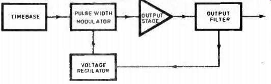
Fig. 6. Block diagram of the inverter
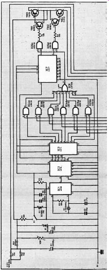
Fig. 7. Complete circuit diagram of the inverter Note that R24 and R25
are rated at 1 Wand R33 must be rated at 7W and be a wirewound (WW) type.
SUPPLY
Capacitor C1 is essential for decoupling the supply when long cables are used between the battery and the inverter.
A small increase in efficiency is obtained by its inclusion, but it may be omitted or replaced with one of smaller value if the cable length is minimized.
The power for the logic and control circuits is supplied via FS3. varistor VDR1 , capacitor C2 and diode D1 maintain a clean, spike free supply for the sensitive CMOS circuits. The logic and control circuits are run at 7.5 volts from a simple Zener stabilized supply comprising resistor R1, Zener diode D2 and capacitors C5, C6.
On/off switching of the inverter is taken care of by switch SI and resistor R3. The switch is a double-pole change over type with only one pole currently connected, the second pole being reserved for use with the U.P.S. add on.
In the off position it shorts the Zener and the logic and control circuits to ground ensuring that any leakage currents in the power stage can not power the low current circuits up. In the on position current is drawn normally via R1 which limits the Zener current.
During operation of the switch there is a brief time when neither way is closed leaving the circuits in a dubious z state, where they are neither connected to the supply nor shorted to ground. To circumvent this highly undesirable condition a resistor R3 is connected across the supply rails and Zener, providing insurance for the CMOS.
TIME BASE
The timebase is designed around three CMOS integrated circuits, IC1 to IC3. IC1, a 4060B, is a 14-stage ripple counter with an on board oscillator intended for direct coupling to an external quartz crystal.
Various division ratios may be obtained by taking the output from any of the ten externally available stages of the counter. In this case a division ratio of 2 13 (4096) is used to obtain a 1 kHz (1 .2kHz for the 60Hz version) output at pin 1 from a 4.096MHz (4.9152MHz for 60Hz output) crystal, X1.
IC2 is a 4516B, 4-bit binary up-down counter with reset. It is used here as a re-setable up counter, counting to decimal 10 (binary 1010), then reset ting to zero and repeating the cycle indefinitely.
==========
COMPONENTS
Resistors
R1 R2, R8, R11, R14,-R17 R20, R23 R3 R4, R5, R7, R10, R13, R16, R19, R22 R6, R9 R12, R15 R18 R21 R24, R25 R26, R27, R32 R28, R29 R30, R31 R33 All 0.25W 5% carbon film unless stated
Potentiometer VR1
Capacitors C1 C2 C3 C4 C5, C6, C13, C14 C7, C8 C9, C10 C11, C12 C15 180 10M (7 off)
1M 10k (8 off)
130 1% metal film (2 off)
150 1% metal film (2 off)
180 1% metal film 1k2 1% metal film 22 1W metal film (2 off)
100 (3 off)
22 (2 off)
1k (2 off)
10k 7W VVVV 4k7 sub min horizontal cermet preset
22,000µ to 47,000p elect. 16V* 220p radial elect. 16V 33p ceramic 47p ceramic 100n polyester 5mm pitch (4 off)
470n polyester 5mm pitch (2 off)
2p2 63V polyester 23mm pitch (2 off)
100n 250V a.c. class X mains rated (2 off)
47p radial elect. 63V
'Value non-critical, may be omitted entirely if battery leads are kept very short ( <1m).
Semiconductors D1, 03, D4, D7, D8 D2, 05
06 TR1, TR2 TR3, TR4 TR5, TR6 TR7, TR8 1N4002 100V 1A rectifier diode (5 off)
BZX88C.7V5 Zener (2 off)
BZX88C.5V1 Zener BC182L npn transistor (2 off)
TIP31 npn transistor (2 off)
2N3055 npn transistor (2 off)
BUV20 npn transistor (2 off), (for 600W see Table 3 next month)
C1 4060B, 14 stage divider with on board oscillator C2 4516B, 4 bit binary counter C3 4514B, 4 to 16 line decoder C4, IC5 4081B, quad 2 input AND gate (2 off)
C6 4078B, 8 input OR/NOR gate C7 40278, dual JK flip flop C8, IC9 LM324, quad op-amp. (2 off)
C10 40106B, hex Schmitt inverter Miscellaneous X1 4.096MHz ±1Oppm stability (for 50Hz), HC-1 8/U crystal, Farnell 170-691; (Alternative for 60Hz)
4.9152MHz, Farnell 103-882 Ti 300 VA Inverter transformer, Jaytee 7E283 (600 VA alternative 9E284)
T2 3 VA mains transformer 0-12V, 0-12V secondaries, AS 207-780 L1, L2 471.tH 2A axial choke ( 2 off)
L3 5.6mH choke: 110 turns 1.2mm enameled wire on EC70 ferrite core, Electrovalue parts, EC70 core B66343-GX127 (2 off), bobbin B66278- B1011T1, mount 866278-B2002 FS1, FS2 15A 32mm fast acting glass fuse (2 off), Maplin 0A33 (see text)
FS3 250mA 20mm time lag fuse FS4 1A 20mm fast acting ceramic fuse, Maplin DA11 Si Miniature d.p.d.t. rocker switch LP1 Green panel mount mains neon lamp PL1, PL2 6-way socket housing for p.c.b. locking connector (2 off), with terminals, (2 off)
SK3, SK4 BS1363 13A cruciform panel mount sockets (2 off)
TB1, TB2 2-way 10 mm pitch (or 3-way 5mm) p.c.b. mount screw terminal connectors (2 off)
Case, 3U 19 inch Rack Case, 32mm screwdriver release panel mount fuseholder (2 off); 20mm screwdriver release panel mount fuseholder; 20mm chassis fuseholder; Heatsinks for TR5 to TR8, 1.85°C/W, Maplin KW50 (2 off); 10mm p.c.b. pillars (4 off); small heatsink for TR3, TR4; connecting wire mains rated 0.74mm2, blue, brown and green & yellow, thin low voltage assorted colors, 2.5mm2, red, yellow, blue and black, 6mm2 black and red, welding cable as required (see Table 2 next month); large insulated crocodile clips, red and black (one off each); heat shrink sleaving, various sizes; T03 silicone isolating kits with bushes (4 sets off); cable ties; M3 panhead screws (12mm, 20mm), plain washers, spring washers and nuts; M3 solder tags (10 off); acetate sheet (see text next month); large self adhesive square feet (6 off). Approx cost guidance only __ plus case
==========
PULSE-WIDTH MODULATOR
The binary output of IC2 appears on pins 6, 11, 14 and 2 and is read by IC3, a 4514B CMOS 4 to 16 line decoder. IC3 outputs 0 to 3 are ignored, with 4 to 9 (pins 8, 7, 6, 5, 4 and 18) being logically ANDed with the regulation control lines by gates IC4a to d and IC5a and b. A reset pulse from output 10 (pin-20) at a repetition frequency of 100Hz (120Hz for optional 60Hz output) is used to reset the counter and toggle the flip-flop in IC7.
The flip-flop performs two tasks, firstly it divides the input frequency of 100Hz (120Hz) by two giving the required 50Hz (60Hz) output and, secondly, provides complementary outputs at pins-1 and 2.
The two remaining AND gates in IC5 are used to AND the outputs of IC7 with the NORed outputs of IC4 and IC5a,b which are logic 1 when their inputs are taken high in turn by IC3 and the regulation control inputs which are controlled by the op-amps in IC8 and IC9.
This obviously gives logic 0 at the outputs of IC5c,d when any of the outputs of IC3 are logic 1. and the appropriate regulation input or pin-17 of IC3 is logic 1. It should be noted that when pin-17 (output 9) of IC3 is high the gating control signal to IC5c and IC5d is unconditionally low and is not affected by the pulse width modulator. This occurs twice per output cycle, allowing a maximum duty cycle of 90 percent thus giving the required dead-time as noted under the section on Pulse Width Modulation above.
VOLTAGE REGULATION
Voltage regulation is by pulse width modulation as already described. The regulation, in this design, is performed in discrete steps by applying simple analogue to digital (A to D) conversion techniques.
The output voltage at the secondary of the power transformer, T1 is monitored using a small mains transformer, T2. The resistor, R33 in series with its primary keeps the current drawn by it down to an acceptable level. Diodes D7 and D8 provide full-wave rectification with the 0V return taken to the centre tap of the secondary winding.
Before the signal can be applied to the A to D converter it has to be smoothed to provide a continuous level for satisfactory monitoring. This is carried out by an RC filter, comprising R32 and C15, with R33 in series with the primary. Adjustment of this voltage is by preset potentiometer VR I al lowing the final output voltage to be set.
Voltage clamping is provided by a simple Zener shunt regulator ensuring that the voltage presented to the operational amplifiers in IC8 and IC9 does not exceed the supply voltage. A stable reference voltage for the A to D converter is provided by D6, a 51 volt Zener diode which has a low temperature coefficient, thus ensuring that the output voltage will remain stable under all normal ambient temperatures.
A potential divider comprising resistors R21, R18, R15, R12, R9, R6 and R30 provides the appropriate reference voltages relating the peak voltage to the r.m.s. value for the respective opamps to monitor. The amplifiers are used in the inverting mode for maximum stability so each amplifier output will swing low when the voltage on its inverting input is higher than the 5.1 volt reference on its non-inverting input.
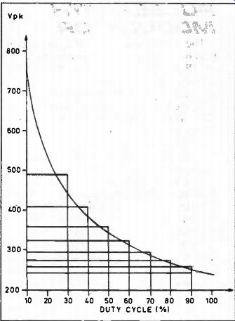
Fig. 8. Step regulation function.
Table 1. Relationship between peak and duty cycle for 240V r.m.s. "square" waves.
To operate the logic correctly and increase (rather than decrease) the pulse width as the voltage falls the output of each op-amp, must be inverted. For maximum reliability Schmitt inverting buffers are specified in IC10 and provide the logic level signals required by the AND gates in IC4 and IC5.
Thus as the peak voltage monitored by the opamps rises the control signals to the AND gates are switched on one by one, reducing the pulse width by 10 percent per gate.
The r.m.s. voltage remains substantially constant while the peak varies since the resistor values specified for the potential divider chain correctly relate the peak voltage and pulse width to its r.m.s. value.
The correct relationship between peak voltage and pulse width are shown in Table 1 for a 240V r.m.s. output at both 50Hz and 60Hz.
PEAK VOLTAGE
A graph of peak voltage against duty cycle for a constant 240 volts r.m.s. is plotted in Fig. 8 as a smooth curve, showing how rapidly the peak voltage increases at low duty cycles. Ideally, these low duty cycles, accompanied by correspondingly high peak voltages, should be avoided wherever possible as they may cause damage to electronic equipment connected to the inverter. The step regulation function also plotted on the same set of axes is shown only from 30 percent to 90 percent, but this will still peak at over 400 volts. In normal operation with the inverter running from a battery which is off charge the duty cycle will stay within the range 50 percent to 90 percent and the peak voltage, from the graph, will remain below 370 volts.
The graph also shows how the voltage can vary within each of the six steps of regulation. The intersection of the vertical lines with the curve gives the peak voltage shown in Table 1 for the particular value of duty cycle. The horizontal lines show clearly the minima and maxima for each regulation point. The 30 percent duty cycle is also shown as having a maxima at approximately 490 volts, which is of course complete nonsense, this point being open ended as the narrowest pulse width avail able to the p.w.m. It does illustrate that, should there be another regulation point below this, its minima would occur at this value. In practice, if a 30 percent duty cycle is ever attained, the peak voltage is unlikely to rise above this value anyway.
The minima for the 90 percent duty cycle is also open ended (at least down to zero volts) but is shown on the graph at 240 volts for similar reasons.
--------
SAFETY
Read this section very carefully before commencing work on the inverter since this project involves dangers of a kind infrequently encountered in home electronics construction.
The electrical safety aspect should be familiar to all but deserves special mention in connection with this project. Although the inverter is in no way connected to the mains electricity supply its output is at a high voltage and low impedance, IT IS EASILY CAPABLE OF DELIVERING SUFFICIENT CURRENT TO KILL! Always switch off and disconnect from the battery before making any adjustments.
Car batteries contain sulphuric acid which is highly corrosive, and great care must be taken to avoid spillage. Spilt acid should be diluted with copious quantities of water and cleaned up immediately. Skin contact should be avoided and is dealt with in a similar manner to above followed by washing with soap. In case of eye contact flush with clean cold water and seek medical attention IMMEDIATELY. The danger of heavily loaded batteries gassing and the consequent explosion risk as mentioned next month in the main text is very real and should not be underestimated. An exploding accumulator can do considerable chemical and mechanical damage.
The electrical energy content of a car battery is very high and, in conjunction with its extremely low internal resistance, can sustain a short circuit current of SEVERAL THOUSAND AMPERES. A spanner placed across the terminals will rapidly become too hot to touch and, when removed, will cause a spark of sufficient magnitude to ignite the hydrogen liberated by the extremely vigorous chemical reactions initiated in its cells!
---------- OUTPUT STAGES
The outputs of the low power circuits used in the timebase and control circuits are incapable of providing more than a few milliamps of output and need substantial buffering before they will drive the power transformer.
Transistors TR1 to TR4 form two Darlington pair emitter followers to buffer the low current complementary outputs of the flip-flop, providing sufficient drive current for the high current output stage.
The power stage is made up of two identical common emitter amplifiers TR5, TR7 and TR6, TR8 driven in anti-phase by TR3 and TR4. A description of either will be sufficient for an understanding of the complete output stage.
Transistors TR5 and TR7 with resistors R26 and R28 form a standard common emitter Darlington stage offering a maximum collector current rating of 50 amps and providing a minimum gain of 400 at a collector current of 25 amps. Diode D3 is included for transistor protection keeping the reverse collector voltage experienced by the transistor below its reverse break down voltage and absorbing high voltage spikes which would otherwise appear on the secondary of the transformer T1.
Base current for the Darlington power stage must be limited to a suitable, safe value and is supplied via a base resistor R24 which allows approximately 215mA of base drive. Bipolar transistors have base capacitance which must be charged and discharged rapidly when the transistor is employed in a fast switching application.
Rapid charge and discharge of a capacitor requires large currents for short periods of time and the 215mA of base drive is inadequate for the required speed.
Shunting the base resistor R24 with a capacitor, C7, will enable a much higher current to flow very briefly as C7 charges and discharges.
Transformer T1 has a centre tapped primary winding with the centre tap (Red) connected to the 12 volt supply rail. TR7 switches one end (Yellow) of the primary to ground for a maximum of 9ms (7.5ms for 60Hz) (subject to p.w.m. permitting) allowing current to flow in half of the primary winding from Red to Yellow. When TR7 switches off there is a minimum period of 2ms (1.67mS) when neither transistor con ducts, this is the reset period for the transformer during which the magnetic field set up in its core can collapse making it ready for the next pulse.
Transistor TR8 provides the next current pulse, which is of the same duration but the current now flows from Red to Blue reversing the polarity of the magnetic field setup in the transformer core by the previous pulse. The induced voltage in the secondary winding follows the alternating magnetic field and has the same period and consequently the same frequency, 50Hz (60Hz).
Table 1. Relationship between peak and duty cycle for 240V r.m.s. "square" waves.
Duty Cycle Pulse Width (50Hz) Pulse Width (60Hz) Peak Voltage.
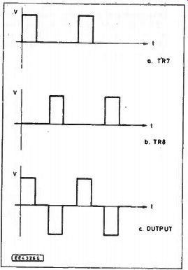
Fig. 9. Waveform synthesis.
EFFICIENCY
Capacitors C9 and C10 perform two functions, improving the shape of the waveform presented to the transformer and increasing the overall efficiency of the inverter. This also reduces the power dissipated in the transistors during the switching time, giving them improved life expectancy.
The turns ratio of the transformer provides a voltage step up to approximately 240 volts and (to comply with the principle of conservation of energy) a corresponding step down in current. In an ideal transformer the power out of the secondary winding should equal the power supplied to the primary, but with unavoidable winding resistances and losses in the magnetic circuit some power will inevitably be wasted, typically 5 or 10 percent.
The relationship between the input waveforms and the induced voltage in the secondary for a 50 percent output duty cycle is shown in Fig. 9. Each transistor is able to operate at a maximum duty cycle of 45 percent when inverter loading and input voltage demand. This, of course, translates to a 90 percent overall duty cycle in the transformer.
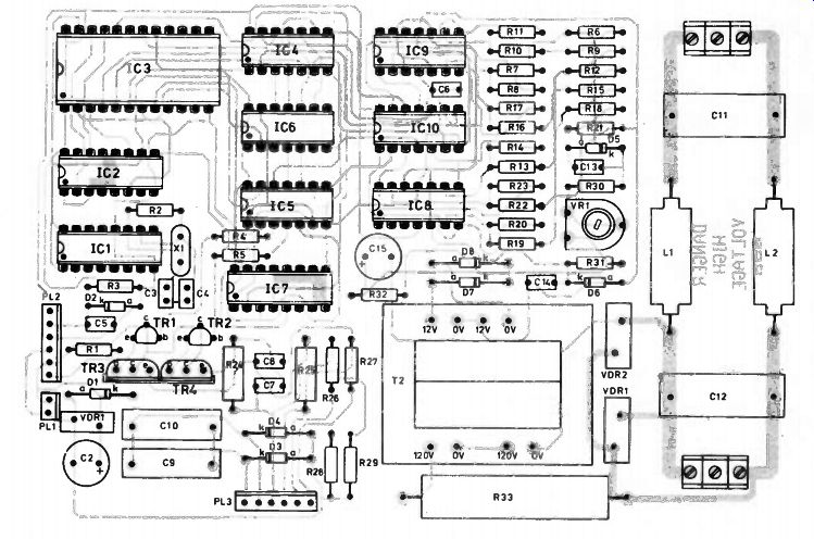
Fig 10. PCB. component layout and (right) the topside and underside
p.c.b. copper foil patterns. Only the necessary part of the topside area
is shown.
OUTPUT FILTER
The waveform at the secondary of T1 is fairly clean and should be suitable for running the majority of appliances. For only a small outlay it is possible to clean it up quite considerably making it acceptable for use with sensitive equipment, such as computers, hi-fi systems and video equipment.
A very simple two stage low pass LC filter connected to the output removes the majority of noise produced by the switching circuits, virtually eliminating any spikes having a fast rise time.
Capacitor C11 and the secondary winding inductance of TI form the first stage of the network removing lower frequency noise while leaving the 50Hz (60Hz) component virtually unaffected.
A second stage comprising miniature radio frequency (r.f.) chokes L1, L2 and a second capacitor C12 remove higher frequency noise including r.f. providing some degree of radio frequency interference (R.F.I.) suppression. Elimination of R.F.I. is essential if the inverter is to be connected to computing equipment otherwise random data loss may occur.
A pair of varistors (voltage dependent resistors) VDR2 and VDR3 clamp the remaining high voltage spikes and can dissipate a considerable amount of energy over a very short period of time.
The resistance of the varistors is normally very high but when the break down voltage is exceeded the resistance falls sharply and literally short circuits the spike before it has chance .to cause damage to the load.
A 5-6mH high Q choke, L3 may be fitted as a final stage filter to remove a large portion of the harmonics present in the square wave output of the trans former, presenting a waveform to the load which should not be too far off sinusoidal.
This will also reduce the ratio of the peak to r.m.s. voltage, particularly with the narrow pulses present under light loading, bringing the peak closer to the 340 volts peak of the normal household mains.
The choke is wound on an EC70 ferrite core which gives plenty of room for thick winding wire, keeping the resistance low whilst providing plenty of inductance.
This gives the inductor a high Q value which aids overall inverter efficiency.
PRODUCTION
The majority of the low power components are mounted on a double-sided glass fiber printed circuit board. Owing to the complexity of this board home production is not recommended for the inexperienced and it is suggested that the EPE PCB Service (code 855) is used. For those who wish to produce their own board the upper and lower foil patterns are provided in Fig. 10.
If you make your own p.c.b. the majority of the holes should be drilled 0-8mm, many of the rest will need opening up to I mm. In general, the pad sizes are indicative of the required hole size, i.e. the larger the pad the greater the hole diameter. A few of the holes should be drilled at 1-3mm, notably for T2, VR1 and the p.c.b. power connectors. The board mounting holes in each corner should be drilled 3mm.
PCB ASSEMBLY
The component overlay for the printed circuit board is shown in Fig. 10 and should be assembled in accordance with the following. Fit and solder all the resistors, capacitors, inductors, connectors, varistors and the preset in place first, leaving R33 until later. The thick tracks around L1 and L2 should be heavily tinned after the components have been soldered in place, as they will have to carry the full output current of the inverter without overheating.
The discrete semiconductors should be fitted next taking great care to correctly position and orientate them in accordance with Fig. 10.
For maximum reliability, and to avoid the necessity for through plating of the p.c.b. holes, the i.c.s are soldered directly into position without the use of sockets.
Eight of the ten integrated circuits are CMOS devices and require special handling (i.e. use an earthed soldering iron and avoid touching the pins). All of the i.c.s are similarly orientated, with pin-1 located top left when in position. Solder two pins at opposite corners on each device and recheck its orientation and positioning before finally soldering the rest of its pins.
Fit the correct crystal for X1 (4.096MHz for 50Hz, 4.9 I 52MHz for 60Hz) and solder it in place very quickly as excessive heating will alter its operating frequency permanently, rendering the final output frequency of the inverter inaccurate.
The small mains transformer, T2 can now be fitted along with R33 which should be spaced 10mm above the board as it will get hot when the inverter is running. Heat resistant sleeving or ceramic spacers should be fitted to its leads before mounting since it will be at 240 volts above ground potential during operation. Note: it is most important for correct circuit function that the specified transformer be used for T2, since its winding resistances come into the regulation equations for the completed inverter.
Next month: The remaining inverter construction details plus setting up, fault finding and modifications.
Acknowledgement: Front cover photograph and text photographs by Ryck Markiewicz.
(adapted from: Everyday Practical Electronics, Dec. 1993)