(adapted from: Everyday Practical Electronics, Jan. 1994)
By MARK DANIELS
A 250 W to 600W design with pulse width modulation for voltage control and an uninterruptable supply add-on. It can also be built for 50Hz or 60Hz operation.
CONSTRUCTION of the Inverter p.c.b. was completed last month. Before continuing check that all components are fitted correctly to the p.c.b. and, if you have not already done so, solder the components to the top foil where appropriate. When the Inverter has been tested the p.c.b. should be given a coat of protective lacquer to prevent corrosion of the copper tracks.
CASE PREPRERATION
This section describes all the case preparation details for the complete U.P.S. since all the metalworking will have to be completed before any components are fitted to the case. If only the Inverter section is being built then some of the holes will be redundant and may be omitted.
Also, two extra holes are required for the battery leads and should be included.
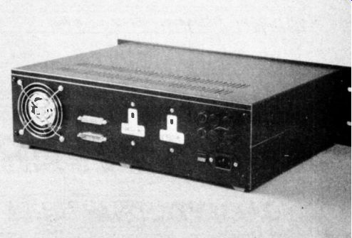
A 3U high 19 inch rack mounting case is specified for the Inverter with U.P.S. since it will give sufficient room for internal mounting of the stand-by batteries and charger circuit. A smaller case may be used as an alternative for the stand alone Inverter, and many suitable metal ones are readily and cheaply available.
All necessary back panel cutouts for the complete U.P.S. are shown on the dimensioned drawing of Fig. II. Before putting drill to metal ensure that all parts can be obtained and the mounting apertures required are identical to those on the diagram. If not, alternative cutouts will have to be made to suit. For the UPS, a 90mm slimline 240 volt fan, an I.E.C. mains inlet connector and a d.p.d.t. mains rocker switch rated at 5 amps (which are not included in the components list for the inverter) are also to be mounted on this panel, so it may be advisable to obtain them before starting the metal working.
The ten 4mm holes may easily be drilled and will cause few problems. The rest of the holes require a little more care and a some what different approach.
To drill six 13mm holes close together in thin sheet steel is asking for problems: the metal will almost certainly buckle, unless securely clamped with the drill mounted in a drill press. It may be wiser to drill small pilot holes and use a "Q-Max" chassis cutter or similar. A 14mm cutter, the smallest size generally available, should prove suitable. Alternatively drill the holes under size and finish with a file.
The 90mm hole for the fan may also be cut using a suitable punch, but being close to the edges of the metal it will generally cause considerable distortion. A better method, in this case, would be to use an electric jigsaw (preferably variable speed). Mask the panel with tape before starting to protect the vinyl finish, mark out the cut to be made and drill a 10 mm hole near the cut line. Clamp the metal securely and, with a fine steel cutting blade fitted to the saw, make the cut very slowly. Do NOT use cutting oil as it may damage the vinyl finish. CAUTION: Always wear eye protection when using a power saw to cut steel.
Punches are available for the remaining cutouts, but tend to be extremely expensive, particularly for the cruciform sockets. Circular 13 amp sockets of 50mm diameter are also suitable and the punches are cheaper so may prove a viable substitute.
An alternative method of making the necessary cut-outs is to mark out the holes and chain drill inside the lines before knocking out the waste. File to the finished size, using the components as a guide.
There are only two components to be fitted to the front panel, but consider able care must be taken to avoid marking the brushed finish when drilling and filing, other than this the same techniques as applied to the back panel may be employed. A suitable front panel layout is given in Fig. 12.
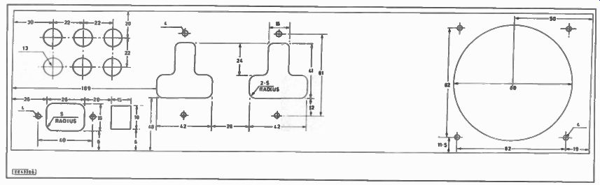
Fig. 11. Back panel cut-out for the U.P.S/Inverter.
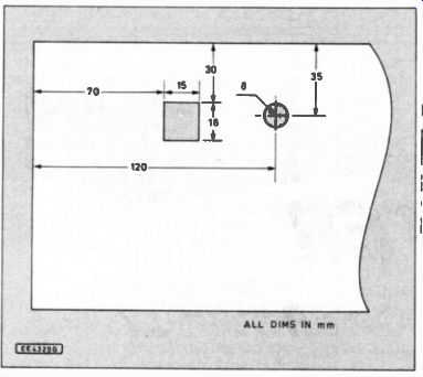
Fig 12 Front panel cutout details.
--------Layout of the back panel for the UPS.
Clean any burrs off with a fine file before lettering the panels then apply two coats of semi-matt lacquer to protect the letters.
Assemble the components to both panels before finally putting the case together in accordance with the manufacturers instructions.
HEAT-SINK ASSEMBLY
Fit a silicone rubber insulating gasket to each BUV20 power transistor (TR7, TR8) before fitting uninsulated crimp type butt connectors (blue insulated crimps may be used if the insulation is removed first) to their emitter pins (see Fig. 13 for pin-out). Crimp the connectors before soldering to ensure a good joint and insulate with heat resistant sleeving where they pass through the heatsink.
Fit a silicone rubber gasket to each 2N3055 (TR5, TR6) and fasten a BUV20 and a 2N3055 to each heatsink with long "top hat" insulating bushes in the heatsink for the mounting bolts to pass through. No heatsink compound is necessary if silicone rubber gaskets are used. Use M3 x 16mm screws inserted from the top side of the transistors with a plain and a spring washer under each nut.
A short length of 20 s.w.g. tinned cop per wire fitted with M3 eyelets at each end should be used to make the connection between the collectors of each pair of transistors. Fit the eyelet between two plain washers and fit a spring washer under the nut. The spring washers must NOT be omitted as the nuts will eventually work loose leading to a non-existent electrical connection and ultimate failure of the expensive output transistors.
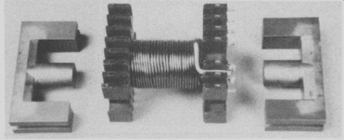
CHOKE CONSTRUCTION
The output filter choke L3 is wound on a large ferrite core with thick enameled copper wire. A single 110 turn winding is wound in four close spaced layers on the bobbin and is terminated at any convenient pair of tags on the bobbin.
The winding direction and precise number of turns is unimportant, four complete winding layers of 1.2mm (or thicker) enameled wire will be adequate. The inductance of the completed choke should be approximately 5-6mH and its d.c. resistance less than 0121.
P.T.F.E. pipe thread tape may be used for covering the winding, applied tightly this will reduce vibration and aid noise reduction although the prototype was left uncovered and produced little noise.
Before assembling the core to the wound bobbin clean the mating faces to ensure a zero gap when finally clamped. This will reduce the possibility of cracking the fragile ferrite core material and reduce buzzing when in operation.
MAIN ASSEMBLY
The case layout for the Inverter components is shown in Fig. 14 and should be adhered to if the U.P.S. add-on is to fit in the remaining space.
The printed circuit board is mounted vertically by means of an aluminum angle bracket, 165mm by 115mm with a 30mm lip along one long side. Four 10mm long insulated pillars are used between the bracket and the p.c.b. with a sheet of insulating material, such as acetate (available from photocopier suppliers or stationers), secured between the p.c.b. and the pillars to prevent possible short circuits between the board and the metal.
The pre-assembled heatsinks can be fitted, with the connections facing out wards as shown, using the pre-punched holes in the bottom of the case and self-tapping screws in the keyhole slots provided in each extrusion.
An optional 80mm fan may be fitted on top of the heatsinks using self-tapping screws in the same keyhole slots as above.
If heatsinks other than those recommended are used an adaptor plate similar to that shown in Fig. 15 will have to be fabricated.
The large electrolytic supply decoupling capacitor C1, if fitted, is fastened to the case with a capacitor mounting clip as shown. C1 is only essential if long input cables are fitted but may be retained with some benefit in other cases. Values between 10,000µF and 47,000µF are recommended, with the larger sizes giving maximum benefit, albeit at a price.
Fit the toroidal transformer T1 between the two supplied neoprene gaskets, with the dished steel washer on the top, and clamp it down with the bolt. One of the pre punched holes in the bottom of the case may be used for the mounting bolt after opening it up to 6mm.
IMPORTANT: DO NOT overtighten the nut as this can damage the insulation on the windings, causing an internal short circuit and ultimate failure of the transformer. Also ensure that the top end of the mounting bolt cannot come into contact with anything electrically connected to the chassis (including the case lid) as this would constitute a shorted turn and cause the transformer to overheat. Do not attempt to make an earth connection via this mounting bolt either as this will have the same effect.
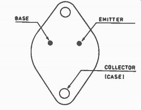
Fig 13. Power transistor connections.
------ Exploded view of inductor L3
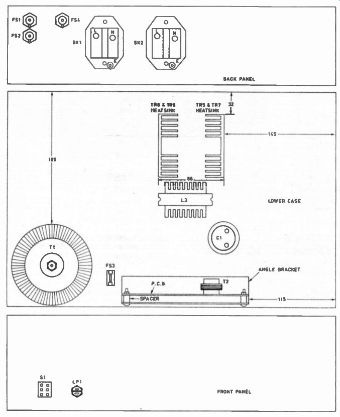
Fig 14. Case layout for the main components.
LOW-POWER WIRING
The main wiring diagram of Fig. 16 shows all the low current connections to be made between the p.c.b. and off-board components using 7/0.2mm stranded wire.
Sensible use of colour coding is recommended as this will ease the task considerably and make fault finding at a later stage much more straightforward.
If p.c.b. plug and socket connectors are used the terminals will need to be crimped or soldered onto the ends of each lead before fitting them into their respective positions in the shell. Ensure that all wires are of adequate length to reach their destinations when correctly routed, they can always be shortened at a later stage.
All six leads from PL2 go directly to the power transistors TR5 to TR8. Extreme care must be exercised when making the connections to these devices since an error here will almost certainly result in one or both of the BUV20's self-destructing at switch on. Sleeve the connections to the transistor pins, preferably with heat shrink sleeving, as a precaution against possible short circuits.
Three of the leads from PL1 go to the main switch S1. Care should be taken to ensure that the correct lead is connected to the common terminal of the switch. Only one pole of this d.p.d.t. switch is presently used, the other being reserved for the U.P.S. circuit to be described next month.
Two of the remaining connections on PL1 are for the 12 volt d.c. supply, which is fused at 250mA in the positive line by FS3.
The other connects directly to the negative supply rail and provides the common return for the logic and p.w.m. circuits. The final connection to this plug provides a 7.5 volt supply to the U.P.S. add-on board to be described next month and should be ignored at present.
HIGH-POWER WIRING
The remaining wiring is high voltage and/or high current and must be carried out in accordance with the I.E.E. wiring regulations for the completed inverter to be electrically safe.
All cables on the high voltage side must be rated for continuous operation at mains voltage and must be suitable for the anticipated maximum current (approximately 1.7 amps). The high current cables in certain sections of the low voltage side may be called upon to carry currents of up to 40 amperes. A minimum cross-section of 6mm^2 is necessary for all internal wiring operating at this current.
The battery leads may need to be considerably thicker and should be chosen ac cording to their length and the recommendations in Table 2.
Flexible cable above 6mm2 cross-section may prove difficult to obtain from your regular electronic component supplier, al though Maplin list some up to 10 mm^2 for use with their high power car audio equipment.
Welding cable, which is ideal, is much more readily available, along with suitable solder lugs, from large motor factors or welding equipment suppliers. This is normally extremely flexible and easy to work with, soldering being accomplished with a gas torch! Large crocodile clips of the type fitted to car booster cables should also be stocked by the same sources and will be ideal for the final battery connection.
All the heavy current wiring is shown in Fig. 17, with appropriate cable sizes indicated. Heavier gauge wire may be substituted, but the indicated sizes should be regarded as an absolute minimum. Keep all low voltage, high current connections as short as possible to minimize cable volt drops.
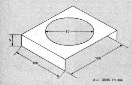
Fig. 15. Adaptor plate for optional fan mounted on the heatsinks--not shown
in photographs.
TRANSISTOR CONNECTIONS
The emitter terminations for TR7 and TR8 are made by crimping and soldering an M5 tag onto the end of a length of 2.5mm wire. The tag may then be slipped onto the bullet connector already attached to the emitter pin of the transistor and soldered in place. A lot of heat is required for this and a soldering iron rated at a minimum of 50 watts will be required.
Keep the iron on the joint until the solder flows around the entire connection, which may take 20 or 30 seconds and although the transistor may get very hot during this operation it will survive, provided it is well heatsinked.
Solder tags (M3) fitted to the blue and yellow leads of T1 will facilitate connection to TR7 and TR8 collectors via the transistor mounting bolts.
Table 2. Cable Size Recommendations.
*Approximate values. + Not recommended.
Specified lengths are total cable lengths, i.e. feed and return.
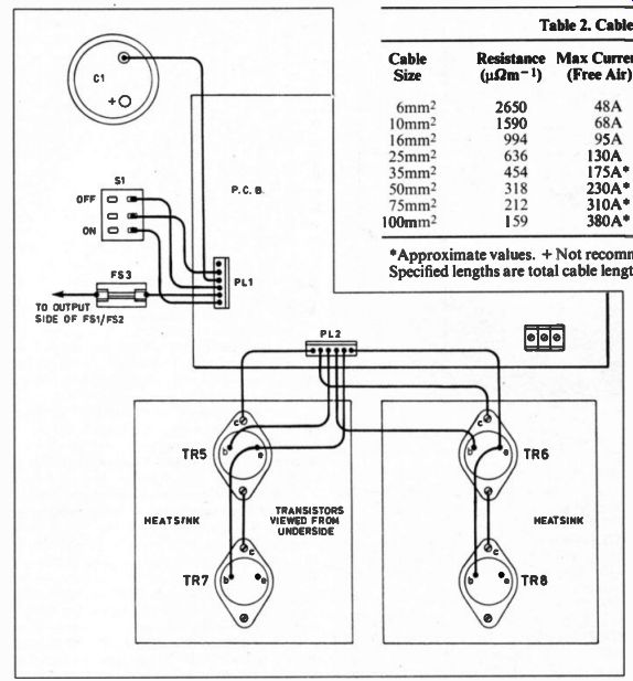
Fig 16. (above) Main wiring diagram.
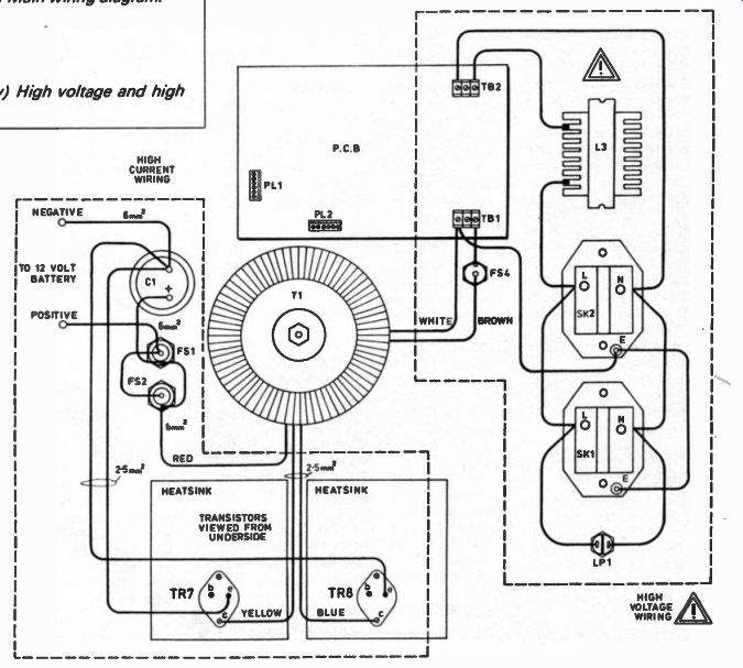
Fig. 17 (below) High voltage and high current wiring.
Use a plain washer either side of the tag and a spring washer under the nut.
If loading is expected to be intermittent or light a 30 amp terminal block, may be used for the connection to the battery leads, otherwise a 50 or 100 amp rating is required. The larger sizes of welding cable (above 10mm^2) will need the 100 amp type to accommodate the conductor size. Most small electrical factors will sell these in one and two-way strips cut from a standard 12-way block.
Large compression type cable glands should be fitted through the back panel to provide strain relief for the battery leads.
The terminal lugs for large welding cables are normally fitted with a special crimping or swaging tool which compresses the soft copper lug around the cable providing a very secure joint. Some of the smaller suppliers will terminate the cables for a small charge.
An alternative method is soft soldering which may be readily carried out at home with a standard full size gas torch. Strip the insulation back approximately 10 mm to 15 mm from the cable end and fit the terminal, compressing it sufficiently with a pair of pliers to grip the cable lightly. Sup port the cable with the terminal uppermost and apply heat to the terminal, taking care not to burn the cable insulation. With the joint up to temperature remove the flame and feed flux cored solder into the joint until it is saturated, re-heating as necessary.
Two meters, or more, of 22 s.w.g. solder may be needed for each joint.
Once cooled the joint should be taped with p.v.c. insulating tape and bolted to the appropriate crocodile clip, slipping the insulated handle grip onto the cable first.
SETTING UP AND INITIAL TESTING
Before rushing out and removing the car battery to test the newly completed inverter spend a few minutes re-checking all wiring and p.c.b. assembly (also make sure removal of the car battery will not affect a coded stereo or the car electronics, which in some case may need expensive resetting if the battery is disconnected). The time spent at this stage could save hours of valuable time and money later--remind yourself how much the pair of BUV20 transistors cost, as these are the most likely components to suffer terminal failure if an error has been made! Read this section thoroughly before proceeding.
Initially fit FS1 in its holder and leave FS2 out. Ensure that the other two fuses are fitted and of the correct rating. Check that the preset VR I is adjusted to the mid point of its travel and that SI is in the "Off" position.
Connect the battery leads to a 12 volt car battery, which is known to be fully charged and in good condition, observing polarity as no reverse polarity protection is provided.
See the Modifications section at the end of this article if this is desired.
Connect a meter set to read 500 volts a.c.
to the output of the inverter and, if avail able, a 30 amp f.s.d. ammeter in series with the battery positive connection. Switch the inverter on and watch the ammeter needle, which should flick momentarily across a large part of the scale before quickly settling down close to the zero. Any reading much greater than two amps indicates a potential fault and the Inverter must be switched off immediately and all wiring double checked.
In practice the off-load input current will probably be 500mA or less.
Check the voltage indicated by the voltmeter, anything in the region 200 to 350 volts is indicative of normal operation.
Adjust the preset VR 1 to obtain approximately 240 volts. With the step regulation employed exact voltages are often unattainable and will vary by a few volts in normal circuit operation, but this is unimportant in this type of application.
Switch off and check the temperature of all the power transistors, including TR3 and TR4 and the small voltage monitoring transformer T2. Also check resistors R24 to R29 and R33, some of which may be quite hot, but not unacceptably so.
If all is well so far, run the Inverter off-load for a minimum period of 30 minutes whilst checking all of the above components for any sign of overheating.
Always switch off before touching anything since mains voltages are present on the p.c.b. and some of the wiring.
LOAD TESTING
Connect a small load of around 25 watts (e.g. a soldering iron) to the Inverter and check the voltage, which may change slightly. Monitor the temperature for a further five minutes before connecting a larger load of around 100 watts (a table lamp is ideal). The power transistors should start to warm up a little now and it would be wise to keep an eye on all high current connections, particularly soldered ones, for any sign of potential failure. Fifteen to twenty minutes should reveal any problems likely to occur at this stage.
Full load for this Inverter is 300 watts continuous and will require FS2 to be fitted for a prospective input current of around 30 amps.
Two table lamps fitted with 150 watt bulbs (the shades will need removing!) will provide a suitable full load test and will require the battery to be in good condition and to have been fully charged for the initial stages of testing.
CAUTION: The battery may gas heavily during this test, producing hydrogen and oxygen which will form an EXPLOSIVE mixture. Do NOT smoke near the battery or produce sparks or naked flames of any kind.
Extinguish any gas soldering irons, even the catalytic types which do not produce an actual flame. Simply disconnecting one of the crocodile clips from the battery before switching the Inverter off will cause a spark of sufficient magnitude to initiate an explosion! See also the section on Safety (last month). A 30 minute continuous full load test should be accepted as the minimum before the Inverter is put into service. The main points to watch are the soldered connections to the BUV20 output devices, FS1, FS2 and the centre-tap of T1. The transistors will get quite hot during this test, but should remain below 85°C at all times. If not, consider upgrading the heatsinks or fitting the optional fan.
The Inverter should be able to maintain at least 220 volts into the load for the full 30 minutes of the test. If it does not, suspect the battery first, then try adjusting VR I slightly to ensure that the maximum pulse width is being obtained. An oscilloscope may be helpful here (see the section on Fault Finding). Note: it may be necessary to adjust VR I to obtain the best regulation across the entire load range.
At this stage it may be prudent to disconnect the Inverter and run the car engine for a while to replenish the charge in the battery. The final test is to use the Inverter with an electric drill under load which will require an input current to the Inverter of around 45 to 50 amps. The prototype was tested using a heavy duty portable drill with a 620 watt motor to bore a 16mm diameter hole through mild steel! The performance was not quite up to mains standard but the task was still completed quite rapidly.
FAULT FINDING
The complete circuit is quite complex and fault finding may be quite a daunting prospect. If the circuit is considered in sections as shown in the block diagram of Fig. 6 each may be individually analyzed in a simple and straight forward manner by referring to the appropriate sections of the text and main schematic of Fig. 7. A multimeter and an oscilloscope are the most useful pieces of test equipment for fault finding on this circuit, without them there is very little you can check.
Before delving into the depths of the electronics check for simple things such as ruptured or missing fuse links, poor battery connections, etc.
If the Inverter refuses to work at initial power up re-check all connections between the p.c.b. and off-board components, then check the p.c.b. for bad joints and incorrectly placed or orientated components. At this stage do not assume that any of the components are faulty. as this is most un likely unless they failed when the circuit was switched on, in which case there is still an error to locate.
Home produced p.c.b.’s are another likely source of errors. particularly when as complex as the double-sided board in this Inverter. Check the p.c.b. against the foil patterns of Fig. 10 and the circuit diagram of Fig. 7 (last month). If FS3 ruptures repeatedly at switch-on it is likely that D1 is connected with the incorrect polarity and should be replaced with a correctly fitted new one. Measure the voltage across the Zener diode D2 which should be 7.5 volts ± 5 percent and compare this with the voltage across the power supply pins of each i.c. in turn. Zero volts at any i.c. indicates a broken or missing track.
Once it is ascertained that power is present at all i.c.’s the inputs and outputs may be checked using an oscilloscope. The output of one should match the input to the next (refer to Fig. 7 to obtain connection details).
LOGIC CIRCUITS
For the logic circuits it is worth noting the following. An AND gate requires a logic 1 (about 7.5 volts) on both inputs to give a logic I at its output, anything else will give a logic 0 (zero volts). The Schmitt Inverters in IC10 change a logic 1 at the input to a logic 0 at the output and vice versa. The NOR gate in IC6 will only give a logic I at its output when all inputs are logic 0, otherwise it gives logic 0. If the Inverter runs but will not regulate the fault is most likely to be around the op. amps IC8 and IC9 or the NOR gate IC6. Check that transformer T2 is giving an output of around 12 volts a.c.
Capacitor C15 should have approximately 12 volts d.c. across it which is regulated to 51 volts ± 5 percent by D6. A voltage of approximately 0.6 volts across a Zener would normally indicate that the diode is incorrectly polarised. Check also that the voltages across the resistors in the potential divider are in proportion to their value.
The power output stage is relatively simple and should not pose any problems.
Simple checking of the connections and security of the joints will usually suffice. It is possible, though unlikely, that a transistor may have failed at initial power up, in which case the following section may provide some fault-finding clues.
COMMON FAILURE MODES
Practical experience with inverter design over a period of several years has generated a list of stock faults and common failure modes. A number of these are presented here, but the list is by no means exhaustive and should not be treated as such.
Failure mode 2 is the most common, occurring in probably 90 percent of cases, fortunately it is also the easiest to diagnose.
1. CMOS devices, when they fail, of ten "crowbar" the power supply rails. To detect which device has failed, once a short circuited supply has been spotted, simply involves measuring the voltage across the supply pins of each chip in turn with a digital multimeter. The failed device will be the one with the lowest supply voltage measured and may be removed, the supply re-checked and a new device inserted.
2. Switching transistor base-emitter junction breakdown is characterized by the other transistor overheating as it drives pulsed d.c. into a low resistance primary winding. If this is not spotted immediately the remaining functional transistor will also breakdown.
When the first transistor fails the tone of the Inverter will change dramatically, from a smooth buzzing to a raspy tone. Switch off immediately to preserve the surviving device.
With the case lid removed it is normally fairly easy to detect which device has failed, since its base voltage will rise taking the voltage across its base-emitter shunt resistor several times higher than normal. The resistor is called upon to dissipate several times its rated power and overheats turning it black or brown. A darkened R28 indicates TR7 failure, likewise with R29 and TR8. Replace both transistor and resistor in each case.
3. Collector-base junction failure is much rarer and is accompanied by a similar change in Inverter tone, but no base emitter resistor darkening.
To determine which device has failed in this case the transformer must be disconnected from the power transistors and the circuit powered up transformerless. Connect a 1k resistor between each collector and the 12 volt rail and use an oscilloscope to look at the waveform across each resistor. The good transistor will produce a reasonable quality square wave on the 'scope, whereas the failed device will produce a straight line at 12 volts.
Fit a replacement BUV20 and re-check with the 'scope before re-connecting the transformer.
4. A timebase failure will often leave one transistor switched off whilst the other drives d.c. into the low resistance primary winding of the transformer.
The Inverter stops functioning immediately in this instance, accompanied by complete silence, i.e. no change in tone first. The failed transistor is located as in 2 or 3 above, but the timebase must be repaired before re-starting the Inverter.
EARTHING (Grounding)
There are a number of ways of wiring the output of the Inverter, including one which requires no earth connection. For maximum safety earthing is necessary in the majority of applications.
The simplest method is to connect one side of the high voltage secondary to mains earth and to the socket outlet earth terminal, as shown in the wiring diagram of Fig. 17. This method may also be used with a properly installed grounding rod where no mains supply is installed. Consult the I.E.E. Wiring Regulations for further in formation on the installation of grounding rods.
Moving motor vehicles require a different earthing method to that described above, since they are not fixed in relation to the ground. In this case the 0 volt (white) side of the secondary should be connected to the negative* battery connection and also to the earth terminal of the socket outlets. A grounding strap, of the type sold as a travel sickness remedy, should also be fitted to the vehicle in accordance with the manufacturers installation instructions to dissipate any static electricity build-up on the vehicle.
It may be necessary to use the Inverter without an earth connection in some circumstances, which will not be described here since they are well known to those who will need this facility. Since a non earthed winding leaves the supply voltage floating it is possible for either side of the supply to be at a high potential above earth (although normally it will also be at a high impedance) it is therefore necessary for BOTH output leads to be fused identically.
The connection between the secondary 0 volt lead and the socket earth terminals should be omitted. If you do not specifically need an earth free supply, or are at all unsure about its application, then you MUST earth the output in one of the ways described above.
A residual current device (R.C.D.) which detects earth leakages and automatically disconnects the supply in the event of a fault would be a sensible addition to the Inverter, particularly in the earth free configuration. All commercial units are supplied with full installation instructions which must be adhered to, further information on installation and use may be found in the I.E.E. Wiring Regulations.
•This applies to negative ground vehicles only. For positive ground systems this connection must be made to the positive battery terminal.
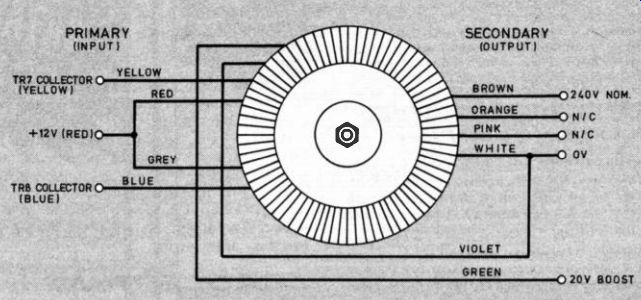
Fig. 18. Connection details of the transformer used for the 600 W version.
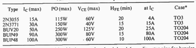
Table 3. Power Transistor Specifications.
*T0204 is identical to T03, with the exception that it has 1.6mm diameter pins for heavier current handling.
MODIFICATIONS
The output frequency may readily be changed to 60Hz for use with American equipment by substituting a 4.9152MHz crystal for X1 as suggested in the text. To obtain 117 volts connect a 240 to 110 volt step-down transformer to the output of the Inverter and adjust VRI to give approximately 117 volts across the 110 volt winding.
For a greater power output a larger transformer will be required, a 9E284 will be suitable for up to 600 Watts. The connection details for this multiple winding transformer are provided in Fig. 18.
The BUV20 output transistors will also need upgrading to BUP49 or BUP48 (see Table 3 for specifications) devices in order to take full advantage of the greater output capabilities. Resistors R24 and R25 will need reducing to 10 or 12 ohms, with a 2 Watt rating. Heatsinks, cables and fuses, etc. will also require appropriate increases in their respective ratings.
The chokes, L I and L2, in the secondary circuit may be retained as they have a maximum rating of 3 amps. It is advisable to reinforce the p.c.b. tracks carrying this current with 20 s.w.g. tinned copper wire to prevent them from melting at full load.
By duplicating R24 to R29. C7 to C12, TR5 to TR8, L1, L2, VDR1, VDR2, FS4 and T1 the control electronics may be employed to drive more than one Inverter. T2 connects to only one of the power transformers. which then becomes the master and has better regulation than the rest. Separate input fuses should also be used for each additional transformer. Up to three slave Inverters may be run in conjunction with one master. If the slave units are to be switched to allow individual control double pole switching of the power Darlington base drives MUST be employed.
All the above components will have to be mounted off the main p.c.b. and TR3 and TR4 will need additional heatsinking. The p.c.b. tracks connecting the power transistors will need uprating with tinned copper wire to provide the extra current handling capabilities required to drive the multiple Darlington power stages. This also applies to the 600 watt single transformer Inverter.
POLARITY PROTECTION
To provide protection against accidental reversed battery connections a 15A stud rectifier should be connected across the centre-tap (red) of T1 and the battery negative lead. The cathode must be positive.
In the event of the battery connections being reversed a large current will flow through the rectifier and cause the fuses FS1 and FS2 to fail and the rectifier to fail to a short circuit. All three components should then be replaced before correctly reconnecting the battery.
REFERENCES AND FURTHER READING
Introduction to Power Electronics. Bird & King
The Art of Electronics, Paul Horowitz and Winfield Hill
Electronic Power Control for Technicians. J R Penketh
Unitrode IC Data Handbook. Unitrode Semiconductor Products Battery to Mains Inverter, EE, March 1990, Self Battery to Mains Inverter Daughter board. EPE, Nov 1992, Self Mains Inverter. ETI, Dec 1992, Self I.E.E. Wiring Regulations. 16th Edition
ACKNOWLEDGEMENTS
The author would like to thank the following companies and individuals for their assistance during the preparation of this article: Peter Godfrey and Andy Sharp (formerly of 1.L.P.) of Jaytee Electronic Services, Tom Peach of I.L.P. Electronics Ltd, Maplin Electronics P.L.C. and Electromail.
Next Month (coming soon): Uninterruptable Power Supply add-on.