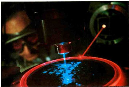
---------- An intense beam of light from a laser scribes microscopic lines
that connect integrated circuits on the surface of a material.
Micro-mounting microchips with a laser-pen
The General Electric R&D Center, Schenectady, NY, has been awarded a 2-year, $790,000 contract by the U.S. Office of Naval Research for this study's further development.
---------------
A microchip can contain tens or hundreds of thousands of transistors in an area the size of a baby's fingernail. Technicians know this. They also know that present-day interconnections, relatively speaking, are bulky: Microchips can be mounted no closer than approximately 1/4-inch.
At General Electric Research and Development Center, scientists are resorting to a laser pen in developing new ways to package more compactly the components of high-speed computers. Using lasers, these researchers draw extremely short, thin metallic interconnections among microchips mounted on a circuit board.
"In the tiny world of microelectronics, that (1/4-inch) is a vast distance," says Dr. Lionel M. Levinson, the R&D Center program manager who heads the laser study. "One result is that signals can spend more time traveling from one chip to another than they do being processed." The goal is to find ways to shrink drastically the distance that an electrical signal has to travel among a computer's various memory, logic and other microchips, thereby increasing the speed at which the machine can process data.
The electrons that comprise a signal hurtle through a computer's circuits at close to the speed of light: 186,000 miles per second.
Because nothing can travel faster than the speed of light, an obvious way to increase a computer's speed is to move its microchips closer together.
Presently, a microchip is mounted in a bulky ceramic package that then is plugged into a printer circuit board. The individual packages are linked together by relatively thick and long electrical conductors printed on the board.
Key to the new approach is the laser beam's intense heat and light, which can trigger chemical reactions in different materials.
The beam can bring about Pyrolysis (heat-induced chemical change) or photolysis (light--induced chemical change). In both cases, the intense laser beam serves as a catalyst. A network of ultrafine circuit lines is created by means of laser-triggered deposition of metal.
The feasibility of this technique, called direct deposition, was demonstrated by R&D center scientists before a U.S. Office of Naval Research contract was awarded. In initial experiments, they succeeded in laying down tungsten lines measuring just one micron across. (One micron is a millionth of a meter, or 1/50 the diameter of a human hair.) An argon laser was employed to draw these fine lines on the surface of a material placed in a sealed chemical vapor deposition cell. After the air was pumped out of the cell, tungsten-hexafluoride gas was fed into it. Then, the laser was switched on and its beam focused through a window in the cell onto the surface.
As the scientists slowly moved the laser beam, its energy caused the tungsten to be stripped from the gas and deposited as a thin metallic line on the surface of the sample. The scientists were able to draw the lines at a speed of several centimeters per second.
In other preliminary experiments, the GE researchers demonstrated that laser deposition also worked with such conductors as zinc, aluminum, molybdenum, platinum, copper and gold.
This technique offers a number of potential advantages over alternative deposition methods. Unlike conventional approaches, it is a low-temperature procedure carried out at atmospheric pressure and doesn't require a furnace. Nor does it need the masks by which circuit patterns are conventionally printed on a substrate. Because only the laser beam touches the surface of the circuit board, the new technique offers the prospect for a quick turnaround time and an ability to drawn lines on surfaces not perfectly flat.
Finally, the laser technique also offers the potential of excellent step coverage, eliminating any breaks or thinning of the circuit lines that can occur when connections are made around corners or from one level to another across the surface of a microchip or circuit board.
Also see: Link |