Inherently rugged, CMOS logic has many advantages over other logic families - high noise immunity and uncritical power requirements are but two. This, the third article in this series deals with counters.
OUR MAIN SUBJECT in this article is counters. It might well be true to say that the range available (compared to TTL) reflects the advances which have been made in other branches of electronics, particularly display technology. BCD counters are conspicuous by their absence as they have generally been replaced by seven segment decoded counters. One disadvantage is a need in many cases for external drivers for LED displays but this will be eliminated when liquid crystal technology is more advanced and, hopefully, cheaper.
BINARY COUNTERS
As usual we will start with the less glamorous devices in the range which, in the present instance, are the straight-forward binary counters. First we should mention the general operating conditions required for all CMOS counters. The clock input rise and fall times should be less than 5 bts and the operating frequency limit is about 2.5 MHz at Vdd = 5 V rising to 5 MHz at 10 V. As far as the problem of drive current is concerned, it is advisable to consult the full data sheets for the device in question but it is reasonable to assume that no trouble is likely to be experienced if the requirement is less than 0.25 mA with a 5 V supply or 0.5 mA with 10 V. Figure 1 gives the pin diagrams for CMOS seven, twelve and fourteen stage binary counters. The outputs are labeled B, with B o the most significant bit ( i.e. giving greatest frequency division). It will be noted that three of the less significant bits are not available as outputs on the 4020A and this limits its usefulness in "divide by N" applications as we shall see later. The greatest division of the input frequency is 128 for the 4020A, 4096 for the 4040A and 16384 for the 4020A. In all cases the counters step on the negative transition of the clock pulse and the reset input sends all stages to logical zero independently of the clock when it is taken high. There is also a twenty-one stage counter (the 4045A) which produces two out-of-phase pulses at separate outputs for every 2097152 input pulses. It is intended for producing one second pulses from 2.097 152 MHz crystals for driving clock circuitry and similar applications.
While we are on the subject of major frequency division chains perhaps we should consider crystal oscillators very briefly. Fig. 2(a) shows one common set-up and it is worth noting that the configuration in Fig. 2(b) is the standard way of producing a simple analog amplifier from a CMOS inverter.
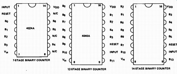
Fig. 1. Three CMOS binary counters.
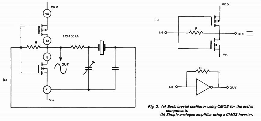
Fig. 2. (a) Basic crystal oscillator using CMOS for the active components.
(b) Simple analog amplifier using a CMOS inverter.
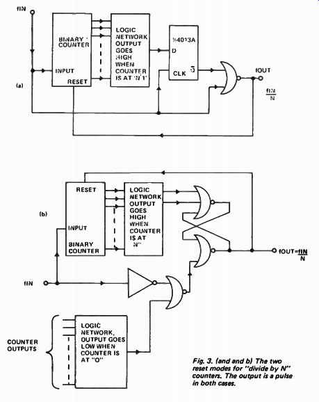
Fig. 3. (and, and b) The two reset modes for "divide by N" counters.
The output is a pulse in both cases.
DIVIDE BY N COUNTERS
There are times when it is required to divide a signal by other than some power of two and by using a 4024A or 4040A we may divided by any number from two to 128 and 4096 respectively, although extra components are required. Figure 3 shows two ways of achieving this end.
The circuit in (a) has the binary counter feeding a system of logic gates, the output of which goes high when the counter reaches N-1 (where N is the number the input frequency is to be divided by). This happens on the falling edge of the clock pulse because the counters are negative-edge triggered. On the next rising edge the flip-flop Ct output goes low and when the clock goes low again the output goes high, generating a pulse of length equal to one half of the clock period which resets the counter. It is interesting to draw a timing diagram for this circuit and prove it works. It should be noted that although the actual output is a positive going pulse, a similar pulse of twice its length ( i.e. one clock period) is available at the Q output of the 4013. A divide by 3600 counter which will provide one pulse an hour from a 1 Hz input is shown in Fig.4 as an example of the technique.
The second mode has the advantage that the "N" count and not the " N-1" count is detected, but two logic networks are required; one to decide when the counter has reached "N" and another to identify the "all zeroes" state and reset the output. It is also a disadvantage in some applications that the counter spends a brief period in the "N" state. It is again interesting to draw a timing diagram and it is worth noting the cross-coupled NOR gates used as an R-S flip-flop. As an example a divide by twenty four counter is shown in Fig. 5 to produce one pulse per day from the one per hour output of Fig. 4 The circuit dissipation of both the counters would be very low ( less than 1 mW) at this low operating frequency and the only note of caution to be sounded is that the counter and flip-flop should not both be triggered from the same edge of the clock pulse ( i.e. one should be positive and the other negative edge-triggered).
A DECIMAL-DECODED DECADE COUNTER
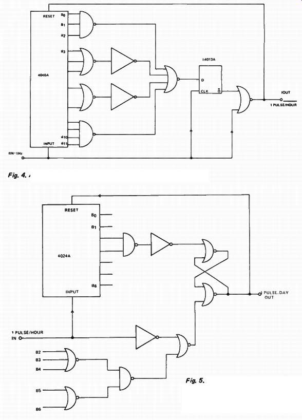
Fig. 4. A divide by 3600 counter using the first reset mode.

Fig. 5. A divide by 24 counter using reset mode two. Note the simplicity that
may be achieved in the logic networks - one NAND gate serves to identify "24".
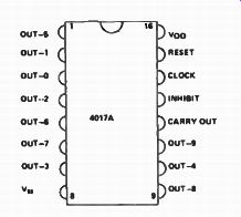
Fig. 6. Pin-out diagram of the 4017A decimally decoded decade counter.
All the old hands at TTL will doubtless be familiar with the 7490 decade counter and 74141 decimal decoder driver. The 4017A combines the count and decode functions in a single package but has the disadvantage of low output drive capability.
Buffering the outputs with 4049A inverters will raise the available output to about five or ten milliamps at supply voltages of five and ten volts respectively. The pin diagram is given in Fig. 6 and the counter advances one on the positive clock transition provided that the inhibit is held low. The reset operates asynchronously when taken high as usual. "Carry-out" may be used to clock the next stage in a multi-stage counter.
This device has fairly obvious applications in controlling switches in multiplying equipment as one and only one output is high at any one time. It is fairly clear also that we may extend the techniques of divide by N counters to cover these devices with the added bonus that they are switch programmable. Figure 7 shows this idea realised using reset mode two because of the ease of switching for N rather than N-1. This circuit has lost an inverter compared with Fig. 5b, this being the change necessary to adapt the circuit for counters and flip-flops which operate on the same clock transition.
The sequence of counters could clearly be extended to any desired length and it is an interesting thought that seven of these counters ( 4017As) and the attendant gates could, when fed with a 1 Hz input generate pulses at any interval from two seconds to over three months! On a more practical note a most versatile digital frequency synthesizer would result if the circuit were used on a phase- locked loop configuration. Remember however that the output is a pulse and it would need squaring (one more flip-flop) before most phase comparators would accept It.
SEVEN SEGMENT DECODED COUNTERS
We mentioned earlier that CMOS IC design reflected the changes in display technology. Two particular examples of this phenomenon are the 4026A and 4033A decade counters with seven-segment outputs. The pin-out diagrams for these devices are shown in Fig. 8 and, as one might guess, the counters are identical, with the exception that the 4026A has a display enable function for use in multiplexing digits and an un-gated C-segment output, whereas the 4033A has ripple blanking and a "lamp-test" facility. We shall consider the use of these special facilities when we have discussed the features common to both. The devices are positive edge triggered and advance only when the clock enable is low. The reset operates when taken high as usual and the segment outputs go high when they are active. Just as in the 4017A the signal at the "carry out" terminal may be used to clock the next stage in multi-decade applications.
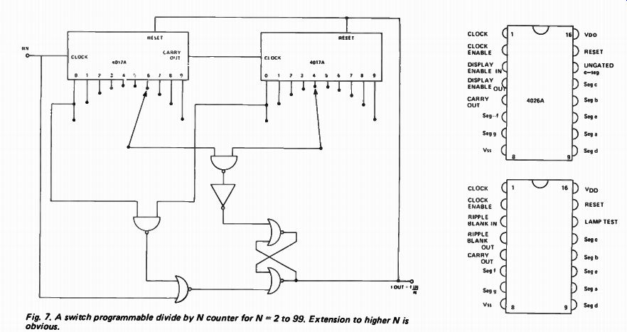
Fig. 7. A switch programmable divide by N counter for N = 2 to 99. Extension
to higher N is obvious.
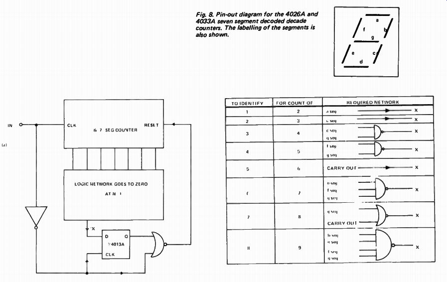
Fig. 8. Pin-out diagram for the 4026A and 4033A seven segment decoded decade
counters. The labeling of the segments is also shown.

Fig. 9. (al How to produce direct seven segment divide by N counters, (b)
logic networks to identify each digit. The extension to a multi decade version
is simple.
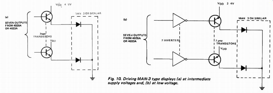
Fig. 10. Driving MAN-3 type displays (a) at intermediate supply voltages and,
(b) at low voltage.
In the same way as we have considered for other counters, the seven segment outputs may be identified by logic gates and the counters made to divide by any number. Figure 9 gives the information necessary and it should be noted that the " N-1 and flip-flop" method is used because the other method does not count through zero.
Now we will have to consider the interfacing of displays with our seven-segment counters. LEDs like the MAN-3 which have a low current will interface directly with the outputs of the 4026A or 4033A and give a tolerable brightness with the available drive current (about 5 mA), provided that Vdd is more than 9 V. If we drop the voltage down to between 4 and 9 V transistors should be inserted, as shown in Fig. 10a, and if the supply drops even lower, the addition of inverting buffers is recommended. The seven transistors needed are generally the components of a single IC. Note also, the discussion on current limiting resistors to follow.