By Bernard B. Daien
ET/D continues its series on the operating principals of the MPU. In this fourth installment the author discusses MPU interconnections, the arithmetic and logic unit, the control unit, and some of the registers In the previous three parts of this MPU series we discussed the role of the MPU, how we can talk to it, and how the MPU receives the information we desire to impart to it. Now we will go on to the next step . .. how the MPU is able to respond to the instructions we give it. In order to do this, we must look a little closer at the "insides" of the MPU ... the different sections that comprise the MPU and how they are interconnected. Two words are commonly used to describe these internals of the MPU, "architecture," or, "organization." They mean the same thing. Now we will proceed to look at some architecture (organization).
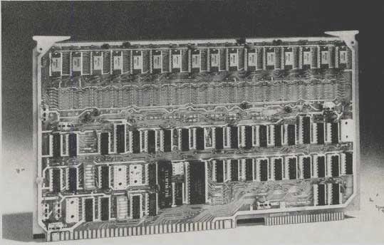
Add on memory. Typical of the multitude of new hardware being developed in conjunction with today's MPU based home and small business computer systems is this board. It contains 32K of RAM for expanding a system's memory and computing capability. This board, from Electronic Solutions, is compatible with Intel's ISBC-80 Multibus and sells for about $1,000.
The bidirectional bus
Information is constantly being put into, taken out of, or transferred between the different sections of the MPU. This is accomplished by means of interconnections called "buses." As pointed out in the preceding article, data is moved around by means of the data bus, which consists of eight parallel lines which can handle an eight bit word in parallel format. Another bus handles memory addresses, and may be a 16 line, 16 bit bus. Commonly there is still another bus, usually less than 8 lines, which handles control signals only, and therefore does not need the capacity of even a one word byte.
Since the MPU is a large integrated circuit, all of the interconnections between the various internal sections are handled via internal buses. (Some of the bus connections are also brought out to terminal pins, so that we have external access to them.) In order to minimize the amount of the IC chip that must be used for the buses, MPUs employ what is known as a "bidirectional bus" system.
This means that signals can move in either direction on a bus . . . sort of like using a single track to route trains back and forth in both directions, between the various stations.
As you will quickly perceive, only one train can use the track at a time, in order to avoid collisions. So it is with the bidirectional bus system . . . only one device is permitted to send information at any given instant. Several devices can "listen," i.e., receive information, from the bus at any instant, since they are not putting signals on the line which can interfere with each other. You should understand this point clearly.
The bidirectional bus is made possible by means of "three state logic" design.
In the usual binary logic, there are only two possible states, a "one" or a "zero," as previously mentioned. A three state device has an extra input terminal, labeled "enable." Using this input terminal, we can apply a "control" signal which for all practical purposes, produces the effect of connecting, or disconnecting the logic device from the bidirectional bus.
Using the railroad as an analogy again, this is similar to shunting a train off the track onto a siding. Actually the train is still in the system, but it is non-existent as far as the main track is concerned. So it is with three state logic circuits. They appear to be out of the bus system when the control signal is in the "disable" mode, and are active in the bus system when the control signal is in the "enable" mode. Physically, the device is still connected, but electrically it has become a complete open circuit and therefore has no more effect on the bus than an open switch would.
Now, can you guess where the control signal comes from, that enables, or disables, the three state logic devices on the bus system? You guessed it . . it comes from the control bus! Let's review the last few paragraphs:
The bus used in MPUs is a bidirectional bus, with signals flashing back and forth on the bus in both directions; and, only one signal can be on the bus at any time in order to prevent interference. This is accomplished by permitting only one device at a time to "send" (transmit) information, although several devices can be receiving information at any moment.
There are actually three separate bus systems in use in the MPU. The data bus handles data, an address bus handles addresses for the many different memory locations (and also the addresses of the various devices on the bus); and the control bus handles the enable signals for the three state logic used and for certain other uses.
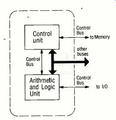
Fig. 1 A block diagram of a microprocessor, also called the Central Processing
Unit, or CPU. The latter terms derives from the earlier days of computing when
the CPU unit was made up of a series of discrete circuits.
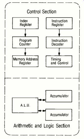
Fig. 2 A more detailed representation of an MPU's interior functions.
Clocking
At this time you will better understand some of the functions of the "clock" mentioned in an earlier part of this series. If you think about it, the enable signals on the control line have to be timed, in a sequence. The clock pulses accomplish this timing (synchronizing) function. Each three state device is timed, in proper sequence, for a predetermined length of time, by ... of course ... the clock! This prevents overlapping of signals, and allocates a definite period of time to perform the required task. Without the clock, the MPU would be just as disordered as you would be, in performing your daily tasks, if you had no clock available.
Let's go further: if you think about it a bit more, you realize the desired logic circuit has to be enabled at the precise moment that the information it receives, sends, or stores, is present. There is no point in enabling a circuit if information isn't available at that instant. Since the clock controls the timing of all information movements, it insures the proper coincidence in time, of all three state circuits on the various buses.
Memories and registers
Now that we know how signals flow, via the buses, we can go on. You will recall that the source program is converted to an object program in binary. This binary program is then stored in some form of external (add-on) memory. Usually, with an MPU, a solid state IC is used as the memory, and information is stored in the form of 8 bit words. Each word in the memory has its own numbered location (addressing). Thus the program stored in the external memory can be quickly retrieved.
The amount of add-on memory that can be addressed is limited by the addressing capability of the MPU. (In the case of an MPU with a 16 bit addressing capability, the maximum number of addresses would be over 64,000 since 16 binary bits is a maximum of 65,536 different combinations.) As the programmer feeds his instructions to the MPU, he assigns memory locations to each in a sequence set forth by the program. Later, when the program is executed, a register, the "program counter," comes into use. This is an internal register which stores the address of the next instruction to be read out of the external memory. As each instruction in the program is read out, in turn, this register indicates where to look for the next instruction in the sequence.
For convenience, this register is abbreviated to "PC." Think of the program counter (PC) as a pointer, used much like the way you use your finger, moving down the lines of a printed page, in sequence, keeping track of the next line you intend to read.
It takes a small, but finite, time interval for the MPU to execute an instruction after it is retrieved from memory. During this time the instruction must be held available until the execution is completed. This is accomplished by storing the instruction, for the required interval of time, in an internal "instruction register." Remember, we previously noted that several registers are used, and that they are named for the use to which they are put. (Some registers are used for several different purposes, depending upon the architecture of the MPU.) The instruction register will be discussed again, later in this article.
So far we have been talking about instructions . . . but what about "data"? Obviously data must also be stored somewhere, until needed. Since data changes, as a result of computations ... this ever changing data must also be stored. For example, if the numbers 5 (data), and 7 (data), are added (instruction), the result is 12 (data). Data is stored in another register . . and this includes input data, intermediate data resulting from an instruction execution, and output data. This register is called "the accumulator." Remembering that the MPU has several registers, the usual use of the accumulator is that numbers in other registers are added to, or subtracted from, the number held in the accumulator . . . and the resulting number is then held in the accumulator during computations. This is true when relatively simple operations are performed, but in executing more complicated operations considerable amounts of intermediate data may be generated, and some of it may have to be stored externally in a "read/write memory." Such a memory is one that we can enter information into . . . read the information out of . . . erase stored information when desired . . . or write new information in when desired. Such memories are also called "random access memories," or "RAM" for short.
As noted above, external memory is often needed to supplement the accumulator when large amounts of data are generated. To minimize this, many MPUs contain several accumulators, enabling faster execution times, and reducing the need for external memory. MPUs often incorporate several registers labeled "general purpose," and these are frequently used as accumulators, as well as for other purposes. They greatly increase the flexibility of the MPU. Some literature refers to such general purpose registers as "scratch pad registers" . . . an apt name. Unfortunately this often leads to confusion in the minds of the student trying to comprehend the architecture of the MPU! Remember, registers are named for the use to which they are put. If the use changes, the name of the register will change, too! Thus, one register may have different titles, depending upon the manufacturer, or the author of the article being read.
Time for review again. We can now perceive that information is put into some form of memory, and held there, until the moment it is needed. The program itself, which is often a long series of steps, must be held in memory, as it is entered step by step. In order to execute the operations called for in the program, we need many memory devices, called registers, which hold information for short periods of time, to enable the completion of each step in the program. We have looked at a few typical internal registers commonly used in MPUs, and we will look at the rest later. Perhaps this is the time to make a block diagram of the architecture of a typical MPU, showing the main parts.
Figure 1 is such a diagram.
MPU versus CPU
Please take note of the fact that the Microprocessor Unit (MPU) is sometimes titled "Central Processing Unit" (CPU). This stems from the fact that in the days before integrated circuits, the functions now performed by the MPU in a computer, were then performed by several separate discrete circuits. Together these circuits were the Central Processing Unit. The CPU, reduced to a single integrated circuit, is today's MPU. This has led to a great deal of confusion for persons attempting self study of the MPU. Simply restated, the functions of the CPU and the MPU are the same. Only the method of construction differs.
As shown in Fig. 1, the MPU, or CPU if you wish, is composed of two main sections, a "Control Unit," and an "Arithmetic and Logic Unit." As shown by the signal flow arrows, signals flow back and forth between the Arithmetic and Logic Unit (ALU), and the Control Unit. In addition, signals flow into and out of the Control Unit and the ALU on the other lines shown, which represent the various buses. If we add some memory, and I/O device(s), we have a basic microcomputer. But, for the moment, let's examine the Control and ALU sections.
The control section
The control section fetches the instructions from memory, interprets them, and is instrumental in carrying out the instructions by sending the proper commands over the control bus, to the other circuitry of the computer. The instructions are executed in the sequence in which they are numbered.
(A number is assigned to each instruction as it is entered by the programmer. The number assigned has nothing to do with the order in which instructions are entered . . . i.e., instruction 4 might be entered before instruction 2, but the instructions will be executed in accordance with the numbers assigned to them.) The ALU section The ALU, as its name implies, performs arithmetic operations (adding and subtracting), and digital logic operations. (For readers who have had previous digital exposure, we are referring to OR and AND gates, etc.) For readers with no digital knowledge, the words "digital logic" mean the electronic manipulation of binary signals necessary to achieve the desired result from the available input signals. The ALU section contains the various registers used for short term storage of data while operations are being executed. For all practical purposes, it can be stated that data handling is performed in the ALU section.
Back to the MPU (CPU)
Together, the Control and ALU sections comprise the MPU ... and they work in a precisely coordinated way. Again, we need a word of explanation. The MPU is a one chip device. The ALU and control sections are convenient concepts, named for the functions they perform.
Literature refers to them in this manner because of a hold -over from bygone days when the MPU was the CPU in computers made of circuit boards with discrete components.
Old ways die hard, often taking many years . . . but since so much of the current literature is influenced by terminology in older texts, and since so many people in the business had their education years ago, it is necessary to deal with the old terms and concepts.
This is a major cause of confusion to the student attempting self -learning, and is one of the reasons for this series.
As a matter of fact, many common terms in electronics had new terms substituted for them when the "digital computer" people succeeded in establishing their own field of electronics. This is part of the ever present effort, in every field, to cloak the new with a "mystique," and thus discourage competition.
Early digital logic gates, for example, were nothing more than simple discrete transistors, used as switches, and could have been mastered by any technician working in electronics . , . but they were presented in such a fashion in the text books on the subject, that most techs were unable to comprehend the material, and were frightened off. As an example, the complexity, and variety of circuits in a color TV far exceeds the complexity and variety encountered in an MPU. MPUs do not deal with microvolt signal levels, or high voltage levels, etc., ad infinitum.
The fact is that this attempt to frighten off techs has been remarkably successful, with experienced techs afraid to get into MPUs, while, peculiarly, young students entering the field find no difficulty in comprehending them in school! With the above in mind, we will go to Figure 2, which is a more detailed illustration of Figure 1, showing how some of the registers, etc., fit into the picture. Some of the labels are strange, but they will be explained as we go along, a bit later, in logical sequence. Of course, it must be understood that the architecture of the various makes of MPUs varies, but the same functions are accomplished by each, just as the various makes of color TV sets varied in the tube complement, type of sound detector, type of AGC, number of I.F. stages, etc. Yet all color TV sets accomplished the same functions, and an experienced technician was able to "follow through" the various circuits because of this. Figure 2 is a composite ...a non-existent "typical" MPU, drawn for model purposes only.
A few more details
It was mentioned earlier that the bidirectional bus was important to the operation of the MPU. A major reason for this is that the larger an integrated circuit is, the greater the probability of a defect occurring in the larger area encompassed. If unidirectional buses were used, there would have to be twice as many of them. Since interconnections have to be made to every section of the MPU, the buses would take up a great deal of chip area.
Bidirectional buses take half as much space.
When we speak of memory addressing, we are talking about finding the location of a memory word (usually 8 bits), stored somewhere inside the memory. Visualize the Post Office box array in your local Post Office. Each box is numbered, in a logical order. So it is with RAM and ROM memories. A coded number is assigned to the location of each memory word, and that word can be located (addressed, accessed) by means of the location number assigned (in binary, of course!). The entering of information into a memory is termed "writing." Retrieving information is termed "reading." Having picked up these details, we can go on to some of the strange boxes on the MPU in Figure 2. Since there are quite a few of these circuits, the ones not covered in this article will be discussed as we progress through this series, therefore it is advisable that you save these issues of ET/D so that you can later refer back to the earlier articles in the series.
At this point, however, the previous comment, that the amount of add on memory is limited by the addressing capability of the MPU, should have significance to you. If the address is a 16 bit address, we can address something over 65,000 locations . . . (usually a bit less, since some addresses are used for other things than memory). And, this is a good example of why you will want to refer back in the text at times.
More registers
We have already mentioned the program counter and the accumulator, so let's look at the "index register" now.
The index register is used to modify the action of the program counter.
You will recall that the program counter points to the location of the next instruction to be executed, as the previous one is executed. Sometimes we may want to change the order in which instructions are executed, instead of progressing in a step-by-step sequence. The contents of the index register can be used to either add to, or subtract from (go forwards, or backwards) the address in the program counter. This gives us needed flexibility, so that we are not locked rigidly into sequence in our programming capability.
The "memory address register" is often not shown on MPU diagrams. It is abbreviated MAR, and usually crops up in that form, without a word of explanation! The MAR stores the MICRO-PROCESSORS continued from page 41 which can be either data, or an instruction. If an instruction location is involved the MAR gets its input from the program counter, but if a data location is addressed, the MAR gets input from the memory.
The "instruction register" is used to store instruction words, the way an accumulator stores data words. When an instruction word is retrieved from memory, it is temporarily stored in the instruction register, until it is decoded and the operation indicated is performed. The instruction word held in the instruction register is decoded by the circuitry labeled "instruction decoder." The word decode as used here means the conversion of the binary data in the instruction word, to a series of operations, in accordance with the intended instruction that was coded (in binary) into that instruction word.
Summary
This article in the series introduced MPU architecture, including the use of tristate devices and the bidirectional bus system. The need for clocking was covered. The program counter, instruction register, accumulator, CPU, ALU, control section, index register, memory address register, and instruction register were defined. The words "addressing" and "decoding", as used in MPU terminology, were explained. Additional background material relating to the MPU was provided.
(source: Electronic Technician/Dealer, Feb. 1980)