This is the final installment of ET/D's series on operational amplifiers. Here we conclude our description of active filters and offer some cautions and troubleshooting tips.
By now you should have a good basic understanding of the significance and use of operational amplifiers and should have the background upon which to build further expertise. You cannot afford to stop learning!
By Bernard B. Daien
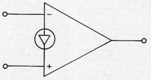
Fig. 1. Parallel resonance -- Note: Both C and L are assumed to be lossless.
The ammeters are assumed to have zero impedance. XL = XC therefore IL = IC
and IG = 0.
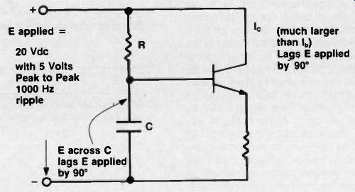
Fig. 2. A power supply active ripple filter.
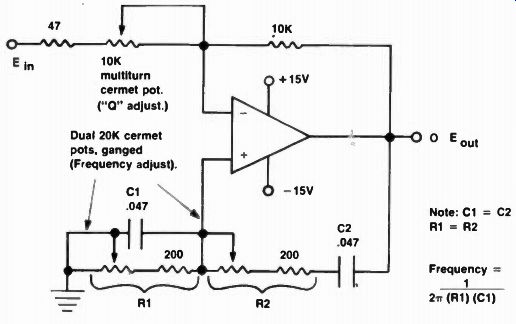
Fig. 3. A practical active bandpass filter. NOTE: All resistors are metal film
unless otherwise indicated. The two capacitors should be polycarbonate film.
mica or Zero coefficient discaps, and matched carefully. Frequency is approximately
200 Hz to 2kHz as shown. Reducing .047 capacitors will increase frequency
accordingly. Thus .0047 capacitors will raise frequency, 2kHz to 20 kHz.
An LM3113, or similar opamp should be used for the higher frequencies This
circuit should be driven by a low impedance generator, such as an opamp or
an emitter follower.
-------
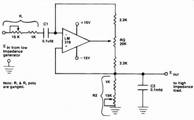
Fig. 4. An adjustable selectivity bandpass active filter. In this circuit
R1 and R2 are always equal and Cr and C2 are also equal.
Frequency can be adjusted by changing R1 and R2, and or by changing capacitors Cr and C2. With the value shown, the resonant frequency is around 100Hz and can be calculated by means of the formula
Frequency r where R is in ohms, and C is in farads
2. (C1) (R1)
The '0". (selectivity) can be set by means of the potentiometer, R0. which is normally near center for 0 100 or so Capacitors should be polycarbonate. mica, or zero temperature coefficient discaps Resistors should be metal film, potentiometers cermet element.
--------
There are several types of circuits which are able to simulate inductance. Known by a variety of unusual names, such as "Gyrators", "Impedance Converters", etc., these circuits are able to make a capacitor/resistor combination look like an inductor . . . (or, conversely, they can make an inductor/resistor combination look like a capacitor). We are primarily interested in simulating an inductor, in active filter applications.
To understand the basic principle of these circuits, study Figure 1, which is a review of basic parallel resonance.
Note that we have an AC generator with a perfect AC ammeter of zero impedance reading the generator's output current. There are two loads connected in parallel with the generator, one an inductor, and the other a capacitor. We assume the inductor and capacitor are lossless, in which case the current through the inductor will lag the generator voltage by 90 degrees, and the current through the capacitor will lead the generator voltage by 90 degrees.
The currents I, and l c are read on zero impedance perfect ammeters.
When XL equals X,, then I L will equal L. Since the two currents are equal, and 180 degrees out of phase, they will "cancel", and the net output current read on the generator output ammeter will be zero. Of course zero current indicates an infinitely high load impedance .... therefore the parallel resonant circuit looks like an open circuit so far as the generator is concerned.
Now then, if we can generate a current 180 degrees out of phase with the capacitive current, when the same voltage is applied to both loads, then the non-capacitive load will "look like" an inductor. Stated another way, if I covered up the inductor in Figure 1, but you were given the facts that the currents I. and l c were equal and out of phase, you would assume that the concealed component was an inductor. Further, looking at the generator current, and noting that it was zero, you would also assume that the circuit was parallel resonant. And, according to accepted theory, your assumptions would be correct.
However, you could be wrong ... if there was an active filter in place of the inductor. With the aid of Figure 2, we can demonstrate how an amplifying element (active element) can be used along with an RC network, to simulate many of the properties of an inductor.
In Figure 2, the ac ripple component is applied to the transistor's base, but the voltage across the capacitor lags the line voltage by 90 degrees. Since there is a resistor in the emitter of the transistor, the transistor base input resistance is very high, and does not load the capacitor down. The base input voltage therefore follows the voltage across the capacitor. The input current of the transistor follows the base input voltage variations. The collector current follows the base current variations, but AMPLI FIED. Therefore the collector current is quite large compared with the current flowing into the R/C network, and the base. Now remember, the base current was shifted, to lag the applied voltage by 90 degrees, therefore the collector current lags the applied voltage by 90 degrees. The net current drawn from the supply line is therefore inductive . . . i.e., this circuit looks like a parallel inductor.
In actual practice we would implement such a circuit with separate dc and ac inputs, and use an opamp instead of a simple one-transistor amplifier. But Figure 2 suffices to illustrate how an amplifier and an R/C network can simulate the performance of an inductor in many ways. It must be pointed out that active filters do NOT have the ability to store energy, thus an "inductor" made of an active filter cannot be successfully used for the inductor in a spark coil (ignition system). On the other hand, series and parallel tuned circuits show normal Q and selectivity, proper phase shift characteristics and energy transfer . . . (but not energy storage), when constructed with simulated inductances.
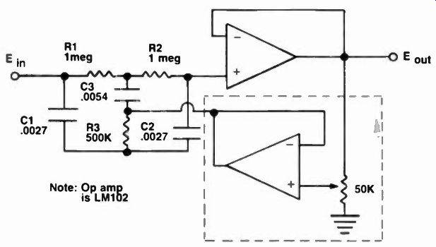
Fig. 5. An adjustable bandwidth notch filter (Twin T configuration). If the
adjustable bandwidth feature is not required, omit components in dotted lines,
and connect junction of R3. C3 to E out terminal. Frequency of operation as
shown is approximately 60Hz. The frequency can be calculated from the formula
… must be equal. R3 must be II, the resistance of Al. Frequency – 2 pi (A1)
(C1)
C1 and C2 must be equal. C3 must be twice the capacitance of C1. Circuit 0 exceeds 50. Component values must be very closely matched for best null, as indicated in text.
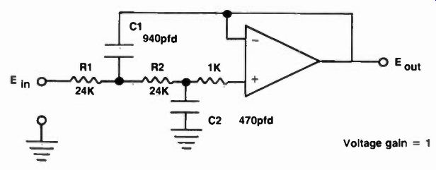
Fig. 6. A low pass filter. Note: Opamp is LM110 or 1556. The frequency of
operation is 10kHz cutoff (knee) of passband, calculated from the formula,
F 1
Notice that 2 pi (R1) \/C1(C2)
R1 must equal R2. and C1 has twice the capacitance of C2. Resistors should be matched to I% or better, capacitors to 5% or better. The closer the matching, the better the performance. Capacitors must be polycarbonate film, mica, or zero temperature coefficient discs. Resistors must be film type. R1 and R2 can be a dual cermet potentiometer for frequency adjustment over a wide range.
Some practical circuits
The following active filters have been chosen for ease of construction. (It is possible to change frequency with simple component value changes only, while some are adjustable by means of a potentiometer, for example). They are all practical circuits that can be constructed by the average technician. Al though there is much literature available about theoretical active filters, very little is directly useable for constructing practical filters (and usually requires matching of components to one tenth of one percent!) Figure 3 is the schematic of an adjustable narrow-band bandpass filter. Not only is the frequency adjust able, but also the bandwidth ("Q"). This circuit offers a Q up to 1000 or more, and gain in the hundreds of times. (The higher 0 settings yield the higher gains.) Unlike most configurations which use more components, and are more difficult to adjust, this circuit is based on the " Wien Bridge", and offers ease of adjustment. For better high frequency performance, try an LM318 opamp in this circuit. Stability depends upon the quality of components used, with polycarbonate film capacitors preferred in the larger sizes, and mica or zero temperature coefficient ceramics used for the smaller values. All resistors should be metal film, while the potentiometers are "cermet" element, multiturn preferred.
Changing the value of BOTH capacitors changes the range of operation, the smaller capacitors providing the higher frequencies.
Figure 4 is the schematic of another bandpass filter with adjustable frequency and bandwidth. This one uses both positive and negative feedback, has high gain, high Q, and the frequency can be readily calculated for your own designs. Large changes in frequency can be made by changing the values of C1 and C2, which must always be equal. Changes in frequency over a ten to one range can be made by means of the potentiometer, which should be a good quality unit, in which the sections track each other closely. As is the case with Figure 3, the input should be driven from a low impedance such as an opamp or an emitter follower. The output of Figure 4 should drive a high impedance, such as the non inverting input of an opamp or the input of an emitter follower. The 1000 ohm resistors are used to limit the range of the pots and are considered to be, with them, single resistors (part of the potentiometer resistances) for frequency calculation.
Figure 5 illustrates a high 0 notch filter (band reject filter). By adding the components in the dotted area, adjust able 0 can be provided. It is best to stay with resistor values between 10,000 ohms and 1 megohm, . . . (we chose the larger value resistors in order to use small capacitors at the low frequency involved). The closer the components are matched to the ratios described in the illustration, the better the null will be.
Figure 6 illustrates a very handy low pass active filter with 40 db per octave roll off after the knee of the curve is reached.
This circuit can be made adjustable by ganging R1 and R2. This circuit is a voltage follower, with unity gain, due to the fact that the output is directly connected back into the inverting input. The output impedance is very low, and will drive most normal loads without problems. The input should be from a low impedance source.
Figure 7 is the same circuit as Figure 6, with the components reversed in order to provide high pass filter action. It is difficult to provide adjustment of frequency, since the two resistors, R1 and R2 are not equal, and therefore tracking becomes a severe problem. (When ganged pots are used in these active filters, they MUST be high grade units in order to provide the stability, and the close tracking required). "Poles", "orders", and decibels . . As you read about active filters in other literature you will find references to "filter poles", "filter order", and "db per octave" ... plus a lot of other terminology that tends to be very confusing.
In a general way, here is how to make some sense of this for practical applications. A "pole" is usually an "RC element" in active filters, thus a filter circuit with one element would have one pole.
The "order" of the filter is directly related to the number of poles . . . it can be said that a two pole filter is a "second order filter", a three pole filter is a "third order filter", etc. The attenuation, or roll off, of a filter is directly related to the number of poles, having 6 db per octave, per pole. Therefore a second order filter would roll off at the rate of 12 db per octave, while a third order filter would roll off at 18 db per octave, and so forth.
As you can readily see, the resistors and capacitors used determine the performance of the active filter ... and often must be very closely matched.
When CDA's are used, the required biasing networks and current limiting resistors pose a problem since they offer parallel resistance networks, effectively upsetting resistor matching, etc.
I strongly recommend that you read the "Linear Applications Handbook", avail able from the National Semiconductor Corporation, at the cost of a few dollars.
It provides thorough coverage of a wide variety of opamp applications, including CDA's and active filters.
Opamp destruction modes It is helpful to know the things that can cause an op to fail. Of course the usual things apply, overvoltage on the supply bus, excessive current due to improper load, etc. However, the opamp is very vulnerable at its input, in two ways. First, the differential voltage between the two inputs cannot exceed the rated value, and second, the input voltage usually cannot be driven higher than the positive supply voltage nor lower than the negative supply voltage. In the case of a single power supply, the input cannot be driven below ground.
Some trouble shooting notes ... As noted in Part I of this series, the input to the opamp is reduced to close to zero when the feedback loop is closed.
The gain of the opamp IC itself is not reduced at all. For example, if we are using an opamp with an open loop gain of 100,000 and a closed loop gain of 100, with a supply voltage of 20 volts, the output signal swing cannot exceed 20 volts and the input cannot exceed 100 microvolts! (20 volts divided by the gain of 100,000.) With the feedback loop closed, the gain will drop to 100, and we can not apply a signal of 200,-000 microvolts (200 millivolts) to the in put because the feedback loop reduces the input signal to 200 microvolts! The signal source resistance must have a fairly high internal impedance, or else we must add a resistor in series with the opamp input, as shown in the schematic of the inverting opamp in Figure 8, in order to prevent short circuiting the signal source by the low input impedance of the opamp. (in the inverting mode only). What happens is that the signal of 200 millivolts is reduced to 200 microvolts at the opamp end of the input resistor, due to the negative feedback.
This reduction of the signal to an extremely low level has led to such statements as, "The inverting input is a virtual ground", implying that any signal fed into it will be reduced to zero. Actually, the signal is reduced to an extremely low level, but not to zero. Many oscilloscopes do not have sufficient gain to see signals below one millivolt, and this can lead the service technician to erroneous conclusions ... like assuming that there is no input to the opamp, when, in fact, the circuit is operating exactly as it should! Even worse, the distortion products fed back into the input via the feedback loop will now be very large in comparison with the reduced input signal, and the input, if it can be seen at all, will appear to be a bunch of spikes, noise, and odd waveforms! In normal use, the opamp has close to zero differential input voltage, due to the action of the inverse feedback. If you open the feedback loop, or ground it out somehow, the differential input can rise in some circuits and exceed the in put rating. Shorting and opening the feedback loop are no-no's in troubleshooting opamps! Well, for the persevering reader who has come through all five parts of this series . . . five months is a long time. All things must end . . . and it is time to end our discussion of opamps. But let me hasten to state that we have only scratched the surface of this vast subject of opamps. Many ingenious circuits exist, and we have only explored a few of the most basic. Hopefully the reader will use this introduction to follow the subject a little further. Most of the opamp manufacturers offer literature, either free, or at very reasonable charge. They are a very good starting point for a basic library about opamps.
Remember, opamps are finding new uses every day, and your study of the subject will certainly find good use both in your work and your personal life.
Where can you buy four versatile amplifiers for around a buck? That has to be the best buy around, and you can bet the electronics industry people aren't losing sight of that fact! Skill in applying opamps can be a very saleable commodity . . . so, sharpen up your op-amp skills.
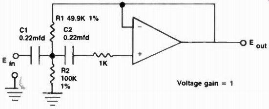
Fig. 7. A high pass filter. Note: Opamp is LM110 or 1556. frequency of cutoff
(knee) of passband is 10kHz calculated from the formula:
F – 1/2 pi (C1). R1(R2)
C1 must equal C2.
R2 has twice the resistance of R1. Resistors should be matched to 1% or better. Capacitors should be matched to 5% or better. Capacitors should be polycarbonate film, mica, or zero temperature coefficient discaps. Resistors should be metal film.
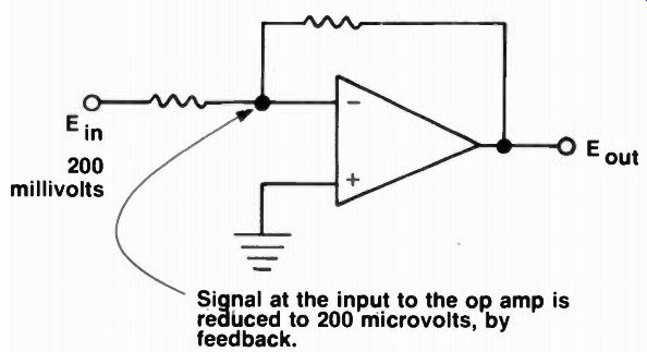
Fig. 8. An inverting opamp. Signal at the input to the opamp is reduced to
200 microvolts, by feedback.
(source: Electronic Technician/Dealer)
Also see: Operational Amplifiers, Part 1