(source: Electronics World, Apr. 1968)

By BENJAMIN BARRON /former Director of Engineering Data and Controls Div.,
Lear Siegler, Inc.
The author received his MEE from Polytechnic Institute of Brooklyn in 1952. His major field of interest has been in solid-state control and servo systems. He has developed various d.c. and a.c. power conditioners for military and aerospace use. He is now Director of Research and Development for Cox & Co.
Guidelines in selecting and specifying the proper d.c. to a.c. inverter and d.c. to d.c. converter, along with precautions in using and designing these sources.
A POWER inverter or converter converts d.c. to a.c. at some point in its operation. The power inverter delivers an a.c. output that is either sinusoidal or some type of switched wave. The power converter, usually called a "d.c. to d.c. converter ", converts d.c. to a.c., transforms the resultant a.c. voltage to another level, and then rectifies and filters the waveform to produce a new d.c. voltage, differing in value from the input d.c.
The inverter may also be used to convert a.c. from one frequency to another. In this case, the input a.c. is first converted into d.c., usually by rectification; then the d.c. is converted into a.c. of another frequency, which is used as output.
Before the advent of power transistors and silicon controlled rectifiers, methods for converting d.c. to a.c. were mechanical, either through the use of mechanical vibrators, motor-generator sets, or power vacuum tubes, thyratrons or ignitrons. Most of these systems were characterized by short life, unreliability, or inefficiency. With the advent of aerospace programs, the need for lightweight, efficient inverters developed. The solid-state or static inverter came into being and has since found application in many other areas.
The most commonly used solid-state devices are SCR's or switched power transistors acting as the power converting elements. This article deals exclusively with circuits using these devices.
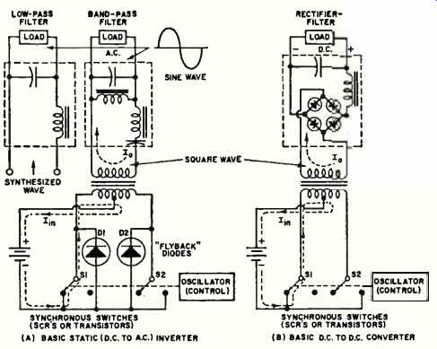
Fig. 1. Basic configurations of (A) inverter and (B) converter.
Direction of electron current flow is indicated by dashed arrows.
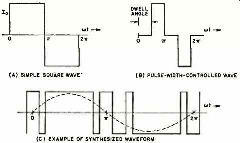
Fig. 2. A number of typical switched waveforms are shown here.
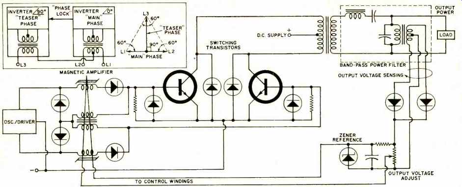
Fig. 3. Simplified schematic of single-phase, pulse-width-controlled
inverter with regulation and sinusoidal output. Inset circuit shows how
two such inverters can be employed to produce 3-phase output.
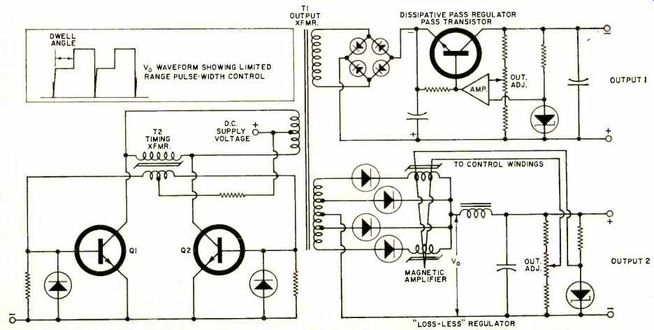
Fig. 4. Self-oscillating d.c. to d.c. converter followed by a dissipative
pass regulator and "lossless" regulator.
Applications of Inverters, Converters
In the missile and satellite fields, static inverters are used as precision a.c. supplies for gyroscopes, accelerometers, synchros, servo controls for guidance and attitude controls, and synchronous motors for timing. In military or industrial areas, static converters are used for: battery or fuel cell-powered emergency supply to critical systems in the event of power-line failure; sonar transducer and driver supply; antenna spinner supply; precision a.c. power for remote clocks; frequency changers for operation of high-speed machine tools; a.c. sources for automotive and marine use; and high-frequency a.c. lighting from d.c. or low frequency sources.
D.c. to d.c. converters are used in missiles and satellites for the conversion of d.c. to one or more isolated levels to be regulated and conditioned in order to power delicate controls and sensing systems. Large converters are used for solar-powered ion engine drives. In military or industrial areas, converters are used for high-frequency, lightweight, high-efficiency power supplies; for portable battery-powered equipment; and in fuel-cell converters and regulators. Converters are used to permit battery operation of portable electronic devices, such as television systems, instruments and recorders, and miniaturized computers and displays.
Operating Characteristics & Circuit Designs
Silicon controlled rectifiers and transistors, when used in the switching mode, have three inherent characteris1 tics that make them suitable for use in the static inverter and d.c. to d.c. converter. They have very low resistance when turned "on" (low forward drop) , very high impedance when turned `off" (low leakage) , and they change state very rapidly. These characteristics result in high conversion efficiency and good load regulation. High reliability is inherent because static inverters and converters have no moving parts, they require no high-temperature heaters in their operation, and the semiconductors are mechanically rugged. Properly designed units, with sufficient protection systems built into them. can stand abuse and mishandling. It can be assumed that they will outlast the systems they are powering.
Both the static inverter and converter use semiconductors as switching elements to alternately connect a load to a d.c. source. Fig. 1 shows the basic configuration.
S1 and S2 represent switching transistors or SCR's that are driven from an oscillator. As can be seen, the input current, Ii,,, is first connected to one half of the transformer primary and then to the other. As a result of this action, the output current from the transformer I. keeps alternating its polarity in synchronism with the driving source oscillator. S1 and S2 may be simply switched "on" and "off," with 180° duty cycle, to produce a simple square wave output. Control of the output can be accomplished by delaying the action of the switches so that the second switch does not come on immediately after the first is turned off. The period of time that is delayed is called the "dwell angle ", as is shown in Fig. 2.
When a sinusoidal output is required from a static inverter. the resultant square wave can be fed through a passive band-pass filter. Other methods are used to produce sinusoidal waveforms. For instance, Si and S2 can have multiple switch actions to produce the quasi-square waveform of Fig. 2C. This is then applied to a low-pass filter. The flyback diode is used here since it is essential to provide a path for reactive current back to the d.c. source. Such current will occur when the load is reactive.
Since the current cannot flow back through the SCR's or switching transistors when their anode or collector voltages are reversed. an alternate path must be provided through the diodes.
In the case of the d.c. to d.c. converter, the square wave is rectified and filtered. If simple pulse-width power control is used, a choke input filter is required.
Fig. 3 is an inverter for aircraft and missile application.
A nuclear-radiation-hardened version is shown on the cover of this issue. The power transistors are switched "on" and "off" by base-to-emitter voltages generated by the oscillator-driver. Magnetic amplifiers are provided in the base circuits of the pair of switching transistors. In this manner, the transistor switching as well as the dwell angle are controlled from a single source. The amount of dwell angle is controlled by output voltage feedback to the zener diode circuit in order to provide the desired output voltage regulation. The resultant pulse-width-controlled wave is filtered to produce a sine :wave output at the load.
It was further desired to obtain three-phase power. To accomplish this, two similar inverters are used and phase locked 90° apart. By suitable interconnection using the "Scott T" configuration, the two phases are combined to produce three phases.
Fig. 4 shows a self-oscillating d.c. to d.c. converter followed by two kinds of post regulators. Timing transformer T2 is designed to saturate readily. The phasing of this transformer is such that the secondary feeds back positively to the bases of Q1 and Q2. The frequency of oscillation is governed by the number of turns, the magnetic properties of the core material of T2, and the value of line-voltage input.
Output #1 is used where d.c. with precise voltage regulation and low output impedance is required. For precise regulation with limited range for the output impedance characteristic, a "loss-less" stepped-wave controller is used (output #2) . The dwell angle produced by magnetic amplifier control over a limited range produces the stepped waveform shown. This type of operation reduces the amount of output filtering required and thus optimizes the response attainable from the pulse-width controller. The output is sensed and compared to the reference zener diode and fed back to the control windings of the magnetic amplifier to accomplish the desired voltage regulation.
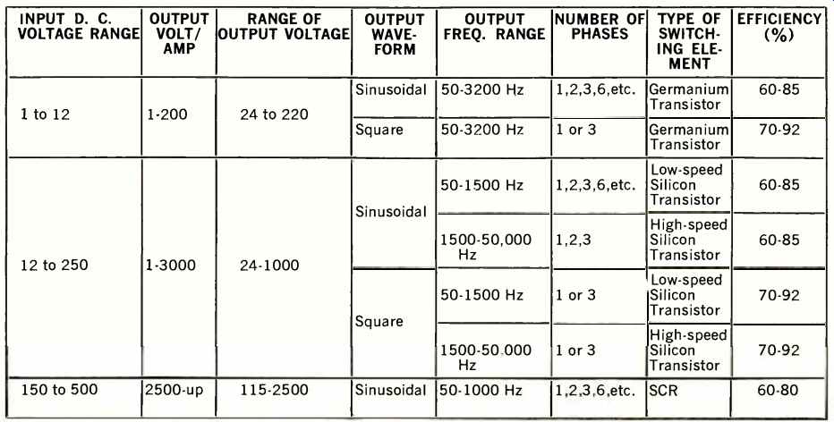
Table 1. Performance characteristics of static inverters with a wide
range of inputs and outputs.
Important Precautions
There are certain precautions to be followed when applying inverters and converters to systems.
1. Adequate cooling: Often the user is vague as to the actual method he intends to use to remove heat from the unit. Some method must be decided upon long before the system is installed. Conduction cooling is done by bolting the device to a surface from which the heat will be removed in some manner (such as with a heat sink) . Thermal characteristic in degrees rise per watt of dissipation into the heat sink must be known and taken into account.
If self-cooling is contemplated, determine if convection cooling is adequate. For inverters over 100 watts. it is usually not adequate. Cooling by radiation is usually useless. If fans are to be used, it should be noted that cooling decreases rapidly with altitude. It is best to select the fan for the maximum altitude condition.
2. D.C. input lines: Such lines are usually highly reactive.
Contrary to the usual assumptions, batteries and d.c. generators are not low-impedance sources for high frequencies.
Furthermore, the inductance of the power line between the d.c. source on the unit is not negligible. The power switching elements pull current from the power line in surges at twice the output frequency. This can give rise to damaging transient voltages on the unit input. In almost all installations, a large capacitor should be included across the d.c. input terminals of the inverter or converter.
Often, it is best to build the line-stabilizing capacitor directly into the unit.
3. Germanium vs silicon transistors: Except for low voltage applications, always use silicon power switching transistors.
4. Grounding: Power switching devices are electrically noisy. They are usually a.c.-coupled to the chassis through the capacitance of the heat-sink insulator and through transformer and wiring magnetic fields. Consequently, short-duration pulse voltages, called "needles ", tend to appear in the outputs of d.c. to d.c. converters. If at all possible, ground the systems to the converter itself.
This is very important when the intended use for the d.c. to d.c. converter is for high-speed digital circuits. Grounding at the converter will greatly reduce these disturbances.
5. Skill of personnel: It is obvious that as the skill of personnel decreases, the chances for mishandling and thus damaging the units increase. This should be taken into account. Careful attention should be given to the specification of the protection systems that must be built into converters and inverters for such use.
6. System discipline: Because of habit, sinusoidal sources are often specified for transformer-rectifier power supplies, the sinusoidal power being produced by a static inverter.
If the ultimate need for the a.c. is for a set of d.c. supplies, either produce the various d.c. levels directly within the d.c. to d.c. converter or supply a pre-regulated square wave to the a.c. distribution system. Maintain control of the d.c. levels required for the circuits being designed by various engineers for later integration into an over-all system. Lack of design discipline usually results in the creation of unnecessarily complex power systems. Multiple-output d.c. to d.c. converters, with the necessary output characteristics, often become nearly as complicated as the systems they are powering. Their cost becomes a significant percentage of the over-all system cost. Whenever possible, the systems manager should specify a minimum number of available d.c. levels before circuit design commences.
7. Specifying: Do not over-specify the output power of inverters or converters. It is a common error for users to assume that an inverter or converter will run much cooler when operated at reduced loading. Losses in a properly designed device vary from about 1.5 to 1 in going from full load to no load. Safety factors are put into the devices when originally designed. Do not call for more accuracy or less distortion than is actually required for the system. Proper specifications result in savings of power, weight, and cost.
Guidelines for Specifying
The following is a list of the critical parameters that should be included when selecting or specifying static inverters (see Table 1) or d.c. to d.c. converters.
A. Output Static Inverter.
1. Volt-amps: minimum, maximum
2. Power factor variation: Minimum, maximum
3. Output frequency: Minimum, maximum. Stability with line, load. temperature, time.
4. Phase: Number needed. tolerance with load unbalance, phase stability with line, load, temperature.
5. Output waveforms: Square: Rise, fall times, flatness, symmetry. Sine: Distortion in percent, maximum percentages for various unwanted harmonics, crest factor.
6. Transient response: Line, load steps.
B. Output-D.C. to D.C. Converter
1. Number of outputs required: Isolation between outputs to ground.
2 Output voltage: Variation of set-point stability with line, load, temperature, time.
3. Output current: Minimum, maximum, ripple content, step variation.
4. Ripple, noise: Maximum in peak-to-peak. Bandwidth to be observed.
5. Transient response: Line, load steps, overshoot, undershoot. and recovery time.
C. Input D.C. Line Voltage: Minimum, maximum, transient surges, line impedance for various frequencies allowable, reflected noise from the inverter back to the line (See the appropriate MIL-Spec, if it is given.)
D. Mechanical: Size, weight, required shape, connectors.
E. Protection: Overload, short-circuit, overvoltage, reverse voltage, over-temperature.
F. Available Cooling: Self-convection, heat sink, fan or air blast, liquid. Define the method.
G. Environment: (See MIL-Spec, if given.)
1. Temperature: maximum, minimum operating and storage. Allowable warm-up time.
2. Shock: Impulse height, shape, time duration, number.
3. Vibration: Sinusoidal, amplitude vs frequency, duration at various frequencies and axis.
4. Random: Bandwidth, spectral content.
5. RFI, EMI: (See MIL-Spec, if given.) Limits of conducted, radiated for various test frequencies.
6. Altitude: Temperature vs altitude.
POTENT POWER PACKS
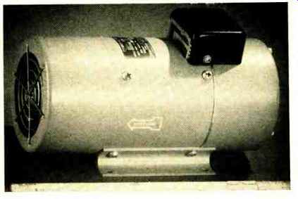
IT is the package that counts, in the air and on the ground.
The problem with most high-current power conversion equipment is that it is bulky, heavy, and hard to manage. In airborne systems particularly, power units often take up most of the available equipment space. One of the companies specializing in reducing the size of power packs is the Tung-Sol Division of Wagner Electric Corp.
The 100-ampere ground power (GP) supply in the photograph is ultra lightweight and compact; it weighs less than eight pounds and is only 8 1/2" l. x 4" w. x 5 1/8" h., although it handles more power than some units twice its size.
Physically, the ground power unit is similar to the airborne version. The cylindrical housing and circular heat sinks, which are constructed of rigid extruded aluminum, enable the power supply to be mounted in any position. An internal blower and a modified pressure cooling system is used to dissipate heat.
Basically, the circuit is a double-Y delta transformer with silicon rectifiers which operate from a 120 /280-volt, 400-Hz, 3-phase a.c. input. Original equipment manufacturers can obtain ground power units having outputs of 28 volts at 100, 200, 300, and 400 amps. Twenty-eight-volt airborne units are available with output currents of 50 to 200 amps. A similarly constructed 60-Hz, 50 to 200 amp unit for portable field use will be introduced.
Communications equipment manufacturers who prefer rack mounted supplies can use the CR 27.5 series of high-current d.c. units. These solid-state controlled magnetic amplifiers were developed especially for marine single-sideband systems. They have a highly regulated (better than 1 %) voltage output of 27.5 V and currents of 25 to 150 amps, and operate from a 50/60 Hz line.
IF it's modules the equipment manufacturer needs, he might try the LC solid-state power packs developed by Electronic Research, Inc. There are five models which cover current ranges of 0-750 mA, and 01, -2,-5, and -10 amperes. Each individual module can be set to any desired output voltage in the 4-32-volt d.c. range.
The LC modular power packs incorporate special circuitry to take full advantage of the properties of silicon semiconductors. The regulator is a silicon transistor emitter-follower circuit in series with the rectified and filtered d.c. source. The series regulator is controlled by a feedback amplifier loop which is referenced to an independent constant voltage source. Changes in the output voltage caused by load variations are compared with the constant voltage source and amplified error signals control the emitter-follower in such a manner as to compensate for the load and line changes. In order to obtain the sensitivity necessary to provide closed-loop regulation, stabilized gain stages are utilized in the feedback loop. The sensing source at the output of the regulator is a bridge circuit with one of its arms containing the constant voltage reference. The referenced voltage is, in turn, provided by an independently controlled zener diode.
The modular supplies range from 4" x 4" x 6 1/2" h. to 8 3/4" l. x 9 1/2" w. x 7 1/4" h. The a.c. input and d.c. output connections are made to terminal strips. Voltage and current adjustments are made on transformer voltage taps and slotted screwdriver adjustments. All models operate at 105/125 Hz, but 400-Hz operation is available by means of a simple tap adjustment.