FM Through Phase Modulation. It was previously seen that, indirectly, frequency modulation is produced when a carrier is phase-modulated.
The development of FM by this method is extensively employed because it is possible to have a crystal oscillator produce the transmitter frequency.
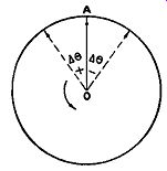
FIG. 16.1. Phase modulation represented by vectors. Delta-theta is the
maximum phase shift of the carrier.
The crystal oscillator not only provides a high degree of frequency stability and accuracy, but it eliminates the need for any frequency-controlling network, such as required in transmitters producing FM directly. In the latter system, it will be recalled, it is not possible to use a crystal in the main oscillator because the FM is produced here.
In phase-modulated systems, the FM is developed beyond the oscillator and crystal control is feasible.
Before we investigate the operation of any phase modulator, let us briefly review the production of FM by phase shifting or phase modulation. Phase modulation is produced when the carrier wave, as represented by vector OA in Fig. 16.1, is made to shift back and forth as it spins around at its fixed frequency. As a result of this shifting, we obtain the same effect as if the frequency were instantaneously being varied. The variation, super imposed on the regular, fixed frequency of the carrier, represents the frequency modulation.
The indirect FM produced depends (1) upon the maximum angle that the carrier wave is shifted, as shown in Fig. 16.1, and (2) on the frequency at which the shifts take place. Mathematically, we can say that:
delta F ( the frequency swing) = f A.0
where f = frequency at which the carrier wobbles or shifts back and forth
delta-theta = maximum angular shift of carrier in radians
This relationship should be kept in mind throughout the ensuing discussion. We will have recourse to it again later in the Section.
Phase Variation. A change in the phase of a signal can be produced by passing the signal through a network containing resistance and reactance. When a voltage is applied to a capacitor and a resistor in series, for example, the current leads the applied voltage by an amount dependent on the relative values of resistance and capacitative reactance. This current develops a voltage across the resistor which leads the applied voltage. If the series combination is considered to be the input, and the output voltage is taken from across the resistor, a definite amount of phase shift is introduced. If the fixed-frequency signal from a crystal oscillator is passed through this network, its phase at the output is shifted by an amount de pending on the ratio of the reactance to the resistance. If the resistor can be varied, the phase angle of the network changes to correspond with the newly established ratio of reactance to resistance. When the resistance is varied with an applied audio signal, the phase angle of the output changes in direct proportion to the audio-signal amplitude and produces a phase modulated signal.
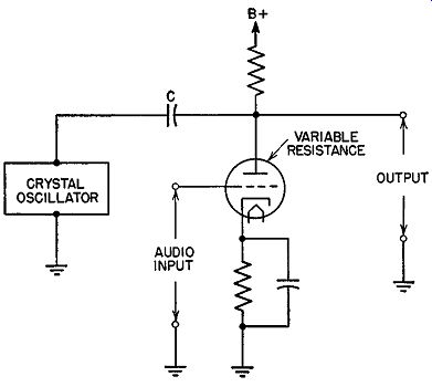
Fig. 16.2. A simple phase modulator.
P-M to FM. The basic circuit of a phase modulator based on this approach is shown in Fig. 16.2. Here, the variable plate resistance of a triode replaces the resistor mentioned above. The plate resistance of the triode changes with grid voltage and therefore serves as the variable resistor.
Since the plate resistance of the triode varies with the audio signal applied to the grid circuit, the phase between the input to the circuit and the output changes with the audio signal. As the grid swings positive, the plate resistance drops and the phase angle of the output increases; when the grid swings negative, the plate resistance rises and the phase angle decreases. The change of plate resistance with various values of grid voltage is exactly proportional to grid voltage over a small range. If the phase angle of the network is changed between wide limits, the amplitude of the output changes. This means that the modulator can produce only a limited phase deviation without distortion. In general, it is reasonably good only over a range of less than 25° of phase shift.
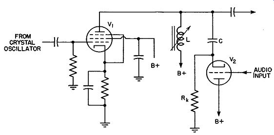
Fig. 16.3. Constant-impedance phase-shift modulator.
Constant-Impedance Phase-Shift Modulator. In order to overcome to some extent the change in output signal amplitude as the phase varies, a constant-impedance network is employed. A phase modulator having such a network is shown in Fig. 16.3. The cathode resistor, Rk, is connected essentially in parallel with the plate resistance of the tube. Rk remains fixed, but the tube plate resistance varies with the audio signal. Since the two are in parallel, the total resistance will vary with the audio signal. however, since only one resistor changes value, the total change will be less than if one resistor alone is employed, as in the previous circuit. It will also be found that the resistance variation with signal level will be more linear.
The inductor, L, in Fig. 16.3 serves to prevent any change in the total impedance, keeping the amplitude of the output constant. For any change in frequency, a change in capacitative reactance is canceled by an opposite change in inductive reactance.
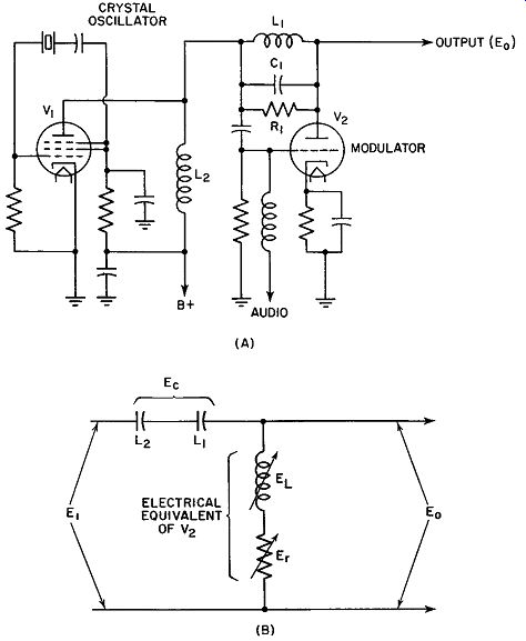
Fig. 16.4. (A) Actual circuit of 6M phase modulator. (B) Equivalent
circuit.
Gm Phase Modulator. Another approach to phase modulation which depends on variations in transconductance is shown in Fig. 16.4A. The output of a crystal oscillator is fed to a modulator, V2, in which feedback exists between plate and control grid. This feedback network, consisting of L1, R1 , and C1 , is tuned somewhat above the operating frequency of the oscillator. Thus, this network presents a capacitive reactance to the crystal signal. Coil L2 , the output load of the crystal oscillator, also is selected to present a capacitive reactance at the oscillator frequency. That is, its resonant frequency is above the oscillator frequency. Under these conditions, it can be shown that the tube itself appears as a series combination of a coil and a variable resistance. (See Fig. 16.4B.) (The latter action, of course, is due to the signal feedback between plate and grid of V2).
The values or magnitudes of the internal resistance and inductance of V2 depend upon the mutual conductance of the tube. The latter, in turn, is governed by the audio modulating voltage applied to the control grid of V2.
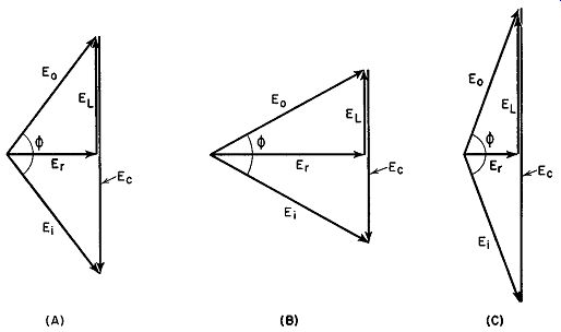
Fig. 16.5. How the voltages vary (with modulation) in the circuit of
Fig. 16.4.
The vector diagrams of Fig. 16.5 illustrate what happens in this circuit.
E, is the input voltage to the modulator from the oscillator. E0 is the output voltage from the modulator. Er is the voltage developed across the resistive portion of the internal impedance of V 2, while EL is the voltage developed across the inductive segment of V2. Finally, E0 represents the sum of the voltages developed across L2 and across L1, R1 , and C1 . When no modulating voltage is present, the vector condition represented by Fig. 16.5A holds.
When the grid is driven more negative, Er increases and the vectors shift to the condition shown in Fig. 16.5B. Finally, when the grid is driven more positive, Er decreases (indicating that the internal impedance of the tube decreases), and the various voltages assume the relationship shown in Fig. 16.5C.
Note the changing phase relationship between E0 and E, in Fig. 16.5.
This can vary between 0 and 180°. Finally, observe that, even with this wide a phase change, E0 remains fairly constant in amplitude. This is a major advantage of this method of phase modulation and considerable use is made of this circuit in mobile communications equipment. Distortion is very low, less than 2i;'o.
Reactance-Tube Phase Modulator. It is possible to produce phase modulation by connecting a variable reactance across the resonant load circuit of an R.F. amplifier (Fig. 16.6). The variation in the phase angle ...
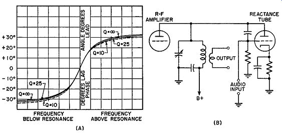
Fig. 16.6. Reactance-tube phase modulation.
... of a parallel resonant circuit shown in (A) is plotted in respect to the frequency. As the frequency of the applied voltage increases, the capacitance in the circuit begins to be predominant, and the resultant total current leads the applied voltage. When the frequency of the applied voltage is lower than the natural resonant frequency of the tuned circuit, the inductance has a lower reactance than the capacitor and, consequently, draws the major share of the current. Therefore, the total current lags the applied voltage.
If the frequency of the resonant circuit is varied and the applied voltage kept constant, the same variation of phase angle is produced. The curve in (A) also applies, except that the center frequency is that of the applied voltage, whereas the frequencies on either side are those to which the resonant circuit is tuned. The circuit can be tuned by changing the value of either the inductance or the capacitance. Changing either at an audio rate with a reactance modulator produces phase modulation. The shape of the phase variation curve depends on the Q of the tuned circuit. This, in turn, depends almost entirely on the construction of the inductor. Therefore, injection of capacitance usually is employed to avoid changes in the shape of the curve.
The reactance modulator, in (B), is designed to inject a variable capacitance across the resonant-circuit load of an R.F. amplifier. Note that plate voltages for the modulator and the amplifier are supplied in common. The injection capacitance changes the tuning of the tank circuit in response to the variations in audio signal. This, in turn, changes the phase angle of the current drawn by the tank. Consequently, the phase angle of the output from the tank circuit also varies. The curve in (A) shows that the change in phase is proportional to the detuning over a small range approximately between the limits of -25° and +25°. This circuit, therefore, cannot produce much phase deviation. It has the advantage of permitting the use of a reactance tube with a crystal oscillator-amplifier combination. However, the wide deviations associated with the reactance modulator when used with a self-excited oscillator cannot be obtained.
Nonlinear Coil Modulator. A coil can be constructed which will have the property, when both radio and audio frequencies are passed through it, of introducing phase modulation into a carrier. Such a coil is called a "non linear coil modulator" (Fig. 16.7A). The output from the R.F. amplifier...
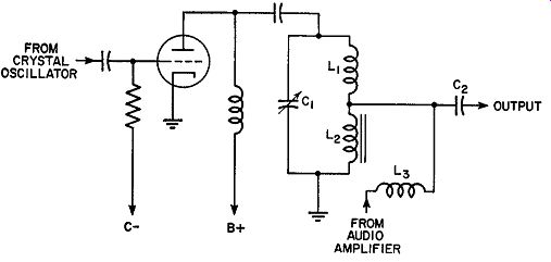
Fig. 16.7A. Nonlinear coil modulator.
...is passed through a plate load consisting of the resonant circuit C1 , and L1, and the special nonlinear coil, L2 . L2 is wound on a special permalloy core together with winding L3 which carries the audio signal from the audio system. The rest of the circuit is a conventional R.F. amplifier. The non linear coil circuit produces a frequency deviation of nearly 1 khz at the output. This phase modulator circuit is relatively efficient in terms of the amount of initial phase deviation.
Normally, when a current is passed through an air-core coil the current flow has the same wave shape as the applied voltage. However, if a magnetic core is inserted into the coil, the situation changes. When a magnetic field exists in a magnetic material, there is a definite magnetizing force corresponding to that field. As the field increases in strength, the material becomes magnetized until a point is reached where the increase in the magnetizing force produces no increase in the magnetic field set up. When the material is fully magnetized and the magnetic flux cannot increase, a state called saturation is reached.
When current flows in a coil, it sets up a magnetic field that magnetizes the core material placed in the immediate vicinity. As the current increases, the corresponding magnetic field increases, as does the magnetization of the core. Because of saturation, however, there is a definite point beyond which any additional current causes no additional magnetization.
Special alloys, such as permalloy, when used as cores reach the saturation point at very low values of the magnetizing field. A coil wound around a permalloy core reaches saturation with a very small amount of applied current. When a sine-wave voltage is applied to such a coil, the magnetic flux increases rapidly until the core saturates; after this, the flux becomes relatively constant.
The relation between the applied magnetizing current and the voltage developed across the coil is shown in Fig. 16.7B. When the current begins to increase to ward its maximum value, the magnetization of the core rises rapidly, with a rapid increase in flux. While the current flow is above saturation (A to B), there is no change in the flux, since the core is saturated. The same situation occurs on the negative half-cycle between points C and D.
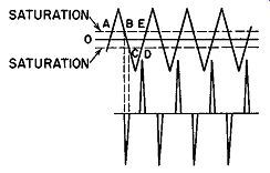
Fig. 16.7B. Voltage pulses developed across nonlinear coil.
The induced voltage depends on the rate of change of the flux. When the flux is not changing, no voltage is induced. In a coil wound on a permalloy core, the flux is changing rapidly during part of the cycle and, during that time, large voltages are induced in it. These voltage pulses of high amplitude occur only during the periods of rapidly changing flux. At other times, when the flux is nearly constant, little or no voltage is induced across the coil. It is shown in the illustration that these voltage changes take place exactly 90° after the current peaks. The polarity of the pulses depends on the direction of the magnetic flux. Therefore, on opposite half-cycles of magnetizing current, the pulses are of opposite polarity. This 90° difference is constant in respect to the magnetizing current, and, since this current is supplied by an R.F. oscillator, the pulse is constant in frequency.
Assume, however, that, in addition to the R.F. energy, audio signals are simultaneously applied to the nonlinear coil. They have the same magnetizing effect on the core material and they combine with the R.F. current to produce the current wave, as shown in the first three lines of Fig. 16.8.
Curve A represents the current in the coil, caused by the carrier R.F. Curve B is the current produced by the modulating signal, assumed to be sinusoidal, for simplicity of analysis. The combined waveform is shown in line C. It is clear that the resultant current no longer goes through the zero axis in the same time interval as before, and, therefore, the region of maximum rate of change of flux is different for each cycle and depends on the audio voltage. These combined currents produced voltage pulses across the coil at different instants during the audio cycle, as in D. The variation ...
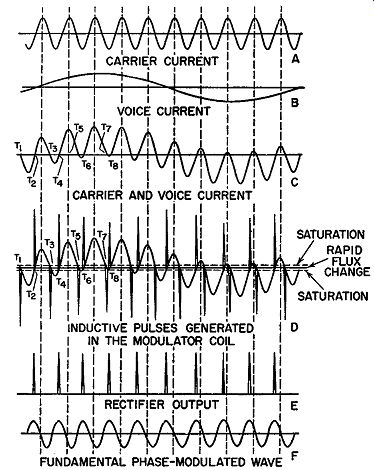
Fig. 16.8. Waveforms developed in nonlinear-coil modulator.
... in the level of the R.F. current at different points of the R.F. cycle causes this effect. Sometimes, the pulse is produced at the normal interval of the unmodulated carrier. At other times, the pulses are spaced more or less than 360° apart. These variations in the spacing of the pulses, with different values of modulation voltages, are obviously equivalent to displacements in the relative phase of the pulses. In other words, a change in the A.F. voltage shifts the phases of the pulses in respect to the phase of those produced by the unmodulated carrier. Therefore, these pulses are effectively phase-modulated.
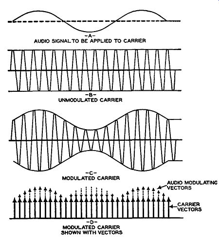
Fig. 16.9.
If the phase-modulated pulses of voltage derived from the nonlinear coil are applied to a rectifier and limiting amplifier, only the pulses of one polarity will be passed. Furthermore, the limiting action will reduce the slight variations in the amplitude of the pulses that appear in D. The action of this rectifier and limiter is shown in E. When pulses of sharp amplitude pass through a resonant circuit, they set it into oscillation at its natural resonant frequency. If these pulses from the output of the rectifier pass through a resonant circuit, which is tuned to their repetition frequency, a sine wave is produced. Since the pulses are phase-modulated by the audio voltage, the resultant sine wave also will be phase-modulated.
Balanced Modulator. A system of phase modulation that received considerable attention from the broadcast industry employs a balanced modulator developed by Major Armstrong. In order fully to appreciate how this system functions, let us vectorially compare AM and P-M. Figure 16.9 illustrates the conventional and the vectorial representation of amplitude modulation. In conventional notation, the low frequency audio signal at (A) varies slowly from 0° to 360°. Directly beneath it, in (B), we have the unmodulated carrier. When the audio signal voltage is applied to the carrier, the result is a modulated signal containing all the intelligence (whatever it may be) of the audio voltage. This is shown in (C). In (D), we have the vector equivalent of the modulated carrier. Note how the amplitude changes at each point, as a result of the addition or subtraction of the audio voltage. Its frequency remains untouched, although, as we have seen, the sidebands formed in this process differ in frequency from the carrier by an amount equal to the audio-modulating voltage.
Fig. 16.10. (A) The separate audio and carrier vectors (OA and AB) and their vector addition to produce P-M. (B) Al) is the phase difference between the unmodulated carrier and the modulated resultant.
In contrast to this, we have the formation of a phase-modulated wave. At each instant during modulation, we must apply the audio-modulating voltage so that it causes the phase of the carrier to advance or retard. It is this shifting, first in one direction, then in another, that is illustrated by the vector in Fig. 16.1. Now, it was noted in amplitude modulation, that the audio voltage increased or decreased the amplitude of the carrier vector. This meant that the audio voltage was being applied either in phase or 180° out of phase with the carrier voltage.
In phase modulation, we do not wish to alter the amplitude of the carrier, merely its relative phase from moment to moment. This phase change can be accomplished by adding the audio voltage vectorially at right angles to the carrier voltage or, electrically, by combining them 90° out of phase with each other.
Let us examine this critically. In Fig. 16.10A, the unmodulated carrier and the audio-modulating voltage are shown separately. If we combine them 90° out of phase as in Fig. 16.10B, then a resultant vector is formed which is displaced from the original position of the unmodulated carrier by some small angle. In other words, by combining the two voltages as shown, we have produced a resultant carrier which is displaced slightly from OA. As the audio signal goes through one complete cycle, its amplitude will vary and, with it, the angular shift of the resultant carrier vector from the position it would occupy if no modulation voltage were present. The variation of the angular shift or displacement at various points in the audio-modulating voltage cycle is shown in Fig. 16.11. Note that the resultant vector (which is the phase-modulated wave) first occupies a position to one side of the unmodulated carrier; then it moves to the other side. In this way it fluctuates back and forth, just as it was pictured in previous discussions. From the wobbling or shifting, an equivalent frequency modulation arises.
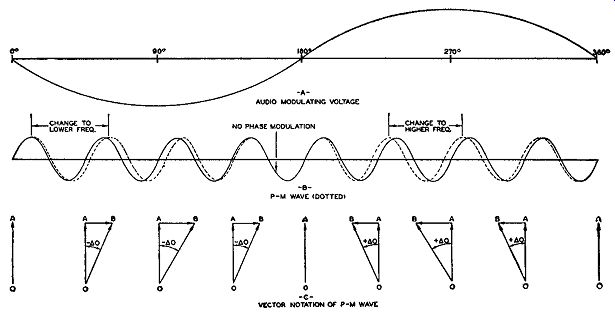
Fig. 16.11. Illustrations of phase modulation.
The formation of frequency modulation, or the variation in frequency in the phase-modulated wave, is clearly indicated in Fig. 16.11. The solid sine wave drawn at the center represents the unmodulated carrier. The other wave, drawn with dashes, is the resultant vector (or the modulated wave) at various instants during the application of the audio signal. At the left-hand side of the diagram the resultant wave is shifted behind the un modulated carrier's position. This means, in effect, a decrease in frequency.
Therefore, the dotted wave, at this point, spreads out (lower frequency) and the maximum peaks are farther apart than those of the unmodulated carrier (shown by the solid lines). When, immediately after this, the audio-modulating voltage drops to zero, the dotted line blends into the solid line, indicating both are of the same frequency. With no audio voltage, there is no modulation.
On the positive half of the modulating cycle, the resultant, or phase modulated carrier, is shifted to the opposite side, indicating that the phase of the carrier has advanced. This is equivalent to a slight increase in frequency, demonstrated by a comparison of the dotted and the solid curves.
We note that the modulated carrier peaks move closer together, effectively increasing the frequency. Finally, at the zero point (360°), the modulation disappears and the phase-modulated carrier is again at its central value.
Armstrong System of FM. In the Armstrong system of FM we do not directly apply the audio voltage to the carrier as shown in Fig. 16.11.
However, we obtain the same results. We start with a fixed source of high frequency voltage, a crystal oscillator (see Fig. 16.12). The output from the ...
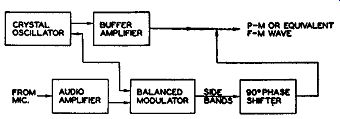
Fig. 16.12. The basic Armstrong system for generating FM waves.
... oscillator is then directed into two different paths. One path contains a buffer amplifier; the other path is through a balanced modulator where the audio-modulating voltage is applied to the carrier signal. At the modulator output, only the sidebands appear. The carrier voltage is suppressed be cause of the operation of the balanced modulator. The sidebands are then shifted in phase by 90° and combined with the unmodulated carrier present at the output of the buffer amplifier. The final result is a phase-modulated wave and, indirectly, also frequency-modulated.
The sideband frequencies obtained from the balanced modulator contain the intelligence of the audio voltage, much the same as though we had amplitude-modulated a carrier. The sidebands are then shifted in phase by 90° and combined with the carrier from the buffer amplifier.
Let us pause for a moment and compare the Armstrong method with the system in Fig. 16.10 for obtaining phase modulation. In one instance we apply the audio-modulating voltage directly to the carrier (maintaining 90° phase relationship) to obtain phase modulation whereas in Major Arm strong's system we use the sidebands produced by amplitude modulation and combine these with the carrier. In both methods, the results are seemingly the same and yet, obviously, both methods are not exactly alike. How does this happen? The answer lies in the fact that Major Armstrong's system is definitely limited in application. First, we can produce phase modulation by applying the audio voltage directly to the carrier. This is entirely analogous to amplitude modulation, except for the manner in which the audio voltage and the carrier are combined. Here, the audio voltage is directly shifting the carrier's relative phase position and, if the system is properly designed, there will be no distortion produced for fairly wide angles of phase shift.
Major Armstrong's method will produce the desired phase and frequency modulation from the combination of a carrier and two sidebands only when the resulting carrier has a maximum phase shift 30° or less. Ex-pressed in radians (one radian is equal to 57.3°) 30° is approximately 0.5 radians. If these voltages are combined so as to give a greater phase shift to the resultant, then along with the phase modulation we have amplitude modulation. This represents distortion and a waste of useful power. But, by keeping the phase shift within the above limits, pure phase modulation is obtained.
It can be shown mathematically that, when a carrier is phase-modulated at angles 30° or less, the resulting modulated wave will contain a total of only two side bands, one above and one below the carrier.
This is shown in Fig. 16.13. Furthermore, each sideband will be 90° out of phase with the carrier. Hence, in the Armstrong system, we take a carrier and separate it into two parts. One part is modulated by the audio signal to produce the necessary sidebands.

Fig. 16.13. A low value of phase shift produces only two sidebands.
These sidebands are then shifted 90° and combined with the remaining half of the carrier (which was fed into the buffer amplifier, Fig. 16.12) to produce the phase or frequency modulation.
To recapitulate, the Armstrong method can be used because:
1. A carrier, phase-modulated at angles of 30° or less, will produce only two sidebands.
2. Each sideband is 90° displaced from the carrier.
In the Armstrong system we take (a) one carrier and (b) two sidebands and combine them 90° out of phase to obtain a phase-modulated wave.
Note, however, that this method is valid only for small phase shifts.
The actual Armstrong unit has the block arrangement shown in Fig. 16.12. The equivalent schematic is shown in Fig. 16.14. The quartz-crystal oscillator operates near 200 khz ( depending upon the assigned frequency of the transmitter), and its output is applied to a buffer amplifier and a balanced modulator. Since the control grids of the balanced modulator tubes are connected in parallel, both grids become positive and negative in step with each other. The modulator plates, however, are connected in push pull, with the plate current from each tube passing through the load circuit coils (L1 and L2) in opposite directions. Thus, in the absence of an audio voltage, each field cancels the effect of the other and no voltage is obtained across La.
Upon the application of an audio-modulating voltage at the input terminals of T1, a varying potential is applied to the screen grids of Va and V4 . Suppose, for example, that the screen grid of V3 is going more positive. At the same time, the screen grid of V4 is less positive since it is attached to the opposite side of the transformer secondary winding. Because of the increased positive voltage, the current in Va will increase while the current in V4 is lowered by a corresponding amount. In a push-pull transformer arrangement, such as we have for L1 , L2, and La, a decrease in one coil, say L2, and an increase in L1 combine to aid each other and to produce a fairly large voltage across La.
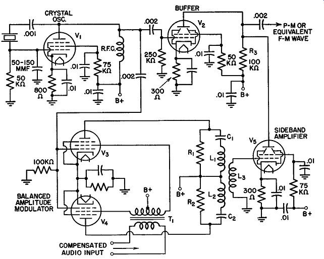
Fig. 16.14. The schematic diagram of the basic Armstrong modulation.
On the next audio half cycle, when the screen grid of Va becomes less positive and the screen grid of V4 is driven more positive, the opposite set of conditions prevails. The voltage across La is also of opposite polarity.
Thus, until the audio voltage is active, nothing appears across La. The effect of the audio signal is to unbalance the circuit and produce the sideband voltages across La.
The arrangement of components in L1 and L2 also produces a 90° phase shift, which is accomplished through the insertion of capacitors C1 and C2 in series with L1 and L2. These capacitors neutralize the inductive reactance of their respective coils ( C1 for L1, C2 for L2 ) and present to the tube a purely resistive load. Under these conditions, the grid voltages of each modulator tube is in phase with its plate current. The plate current, in flowing through the load, will develop a magnetic field about each coil. The variation of a magnetic field is directly dependent upon the current that produced it. Hence, the control grid voltage of each tube, the plate current of that tube, and the magnetic field set up about the coil are all in phase.
The magnetic field, in cutting across L3, will induce a voltage. From elementary a-c theory we know that an induced voltage is maximum when the magnetic flux lines arc changing most rapidly. This rapid change occurs when the field is going from positive to negative (or negative to positive) values. However, the induced voltage is minimum or zero when the flux is hardly changing at all. This absence of change occurs at the positive and negative peaks (sec Fig. 16.15). If we plot the relationships of induced voltage to magnetic flux variations, we immediately see that a phase difference of 90° is introduced. In this manner we produce the necessary side bands and shift them 90° with respect to the crystal oscillator carrier.
Tube V5 amplifies the sidebands and combines them with the carrier.
Resistor R3 is the common load for V2 and r 5 , and it is here that the combination of carrier and sidebands takes place.
Frequency Swing Compensation. Thus far, we have been concerned solely with the stage or stages where the phase modulation occurs. Once this is achieved, however, the next step is frequency multiplication, not only to raise the carrier frequency to the desired value, but also to increase the band width occupied by the signal. However, before frequency multipliers ~re considered, it is first necessary to determine how much frequency shift is produced by a certain phase change. For this, we refer again to the equation: t::.F = f·t::.8
where f = frequency of audio modulating voltage
delta . theta = maximum phase shift in radians.
Actually, in the foregoing equation, delta . theta should be delta . theta sin 2wft because the angle varies from instant to instant. However, we are interested only in the maximum value of the phase swing; hence we use t::.8. The maximum value of sin 2wft is 1, and delta . theta X 1 is t::.8. delta . theta should be expressed in radians; which is, as we have seen, equal to the angle in degrees divided by 57.3; f is expressed in cycles.
Let us assume a maximum phase swing of 30° is produced in the phase modulator. At the highest audio frequency, utilizing the full phase swing of 30° (0.524 radian), the equivalent frequency swing or variation is:
AF = 15,000 X 0.524
AF = 7860 cycles
AF= 7.86 khz
Now, let us see what happens when low frequency audio signals are applied.
The lowest audio frequency desirable is generally 50 cycles. Substituting this in the equation, AF= 50 X 0.524 AF = 26.2 cycles
Note that both signals gave the same phase swing, yet the low frequency voltage produced a frequency variation of only 26.2 cycles whereas the highest audio frequency produced a frequency variation of 7 .86 khz.
Suppose we transmitted the carrier with these frequency shifts. At your receiver, which would give the greatest output? The 7.86 khz, of course, since all FM receivers develop a greater output for a wider frequency swing. But this does not represent the conditions at the transmitter. Here, both signals were equally strong. Something, then, must be done to place both signals, or all frequencies for that matter, on an equal footing. No matter what the frequency, signals of equal amplitude should produce equal frequency shifts.
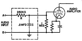
FIG. 16.16. A pre-distorter network.
To achieve this, a pre-distorter circuit is inserted in the audio amplifier stages (see Fig. 16.16). The resistor R is made very large in comparison to the reactance of capacitor C at all audio frequencies. This means that for any voltage impressed across terminals A, B, the current will be deter mined by the resistor R. The effect of C is negligible. Thus, no matter what the audio frequency, the same voltage will produce the same current through R and C. Across C, the voltage will depend upon the frequency. A higher frequency will develop less voltage across C than a lower frequency. This is because the capacitor offers less opposition to higher frequencies. Hence, we obtain the desired inverse effect to counterbalance the rising f effect of phase modulation. The pre-distorter components of R and C apply less high frequency voltage to the grid of the tube. (In the phase modulators previously shown and discussed in this Section, no such network was shown, but in each case one would be included.) Since the low frequencies produce the smallest equivalent FM, the audio-correction network reduces the effect of all frequencies higher than the lowest audio frequency-say, 50 cycles-so that, in the end, all the frequencies of the same strength will produce the same frequency modulation. The amount of equivalent FM, then, that a 50-cycle voltage produces will determine how much multiplication is to be applied to obtain the final FM swing.
Let us return to the circuit of Fig. 16.14. Utilizing the maximum phase shift of ±30°, we discovered that, at 50 cycles, the carrier has a frequency variation of ±26.2 cycles. The carrier frequency, at this point in the circuit, is the crystal oscillator frequency. For the circuit of Fig. 16.14, as employed in commercial FM broadcasting, this frequency value would be around 200 khz. Hence, our FM signal is 200 khz with a frequency swing of ±26.2 cycles.
What we desire, at the antenna, is the assigned station frequency, say, 90 mhz ± 75 khz. The problem is to increase the 200 khz ± 26.2 cycles to 90 mhz ± 75 khz. In order to deal with round figures, let us change the 26.2 cycles to 25 cycles.
Frequency Multiplication. If we divide 75,000 cycles (the desired frequency swing) by 25 cycles (the swing we now have) we see that a frequency multiplication of 3000 (75,000/25) is necessary. Although it may be a trifle difficult to have exactly a 3000 increase using triplers and doublers, we can get very close, say, 2916. This frequency multiplication is possible if we use the following assortment of doublers and triplers: 2, 3, 3, 3, 3, 3, 3, 2. The signal is passed through successive stages until the total multiplication of 2916 is obtained.
The frequency multiplication is applied not only to the frequency swing (the sidebands) but also to the carrier. This means that the original 200 khz of the mhz--resulting in a value considerably above the desired 90 mhz. Something must be done to prevent the carrier from rising to a frequency higher than its assigned frequency, in this case, 90 mhz, and, at the same time, to obtain the maximum frequency deviation of ±75 khz for the sidebands.
A method to accomplish this is shown in Fig. 16.17. The entire transmitter is arranged in block diagram, with each unit numbered for easy identification purposes. At the input to the amplifier in block No. 6, the equivalent frequency modulation has been achieved. Thereafter, the carrier and its sidebands are sent through a series of frequency multipliers until, by the time the mixer is reached (block No. 13), the carrier has been increased to 32.4 mhz and the frequency variation to ±4.05 khz. Note that at the input to the mixer the carrier is 32.4 mhz whereas at the output it has been reduced to 5 mhz. The reason is the mixing action within the tube.
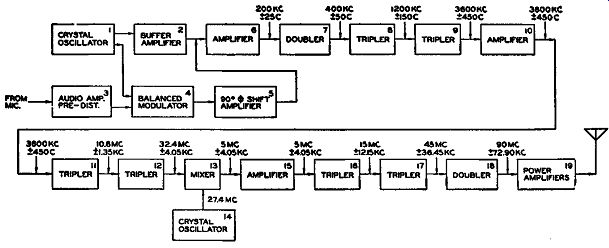
Fig. 16.17. A complete block diagram of the basic Armstrong FM transmitter.
Whenever we mix two signals, the output consists of the original two mixing frequencies and the sum and difference frequencies. Of primary interest is the difference frequency, 5 mhz. To accentuate this frequency and minimize or eliminate the others, we place a resonant circuit at the output of the mixer which is peaked at 5 mhz. With this simple arrangement it is possible to reduce the original carrier to the point where it can be further increased to the desired 90-mhz values.
But what of the sidebands during this process? The incoming signal to the mixer has a frequency variation of ±4.05 khz. The range, then, of the input signal is from 32.39595 mhz (32.4 mhz - 4.05 khz) to 32.40405 mhz (32.4 mhz + 4.05 khz) . We change 4.05 khz to 0.00405 mhz and then add and subtract this figure with 32.4 mhz to arrive at the foregoing values. When the 27.4 -mhz mixing frequency is added, the following output difference frequencies are derived:
32.39595
-27.40000
4.99595
32.40405
-27.40000
5.00405
... or, what is the same thing, 5 mhz ± 4.05 khz. Look at this carefully for it demonstrates clearly that by mixing it is possible to lower the carrier frequency and, at the same time, retain the original frequency variation.
Hereafter, the tripling and doubling sequence is straightforward until we arrive at the 90 mhz ± 72.9 khz. By assuming a starting frequency variation of 25 cycles, we obtain only a ±72.9- khz frequency shift at the output.
However, with the 26.2 cycles proposed originally, we would come much closer to ±75 khz. In any event, we do not have to hit it exactly on the head.
Anything slightly less is still quite satisfactory.
There is one more fact to be noted concerning the Armstrong transmitter.
In addition to the audio pre-distorter, or audio-correction network, recently discussed, we also require a pre-accentuator. The pre-accentuator is used here as in the reactance-tube FM transmitter, namely, to raise the level of the higher audio tones in order that they may be in a better position to combat the effect of noise at these frequencies. At the receiver, a de-accentuator or a deemphasis circuit returns the higher frequencies to their proper level.
Do not confuse the purpose of the two circuits. The audio correction net work is needed to counteract the tendency of the higher frequencies to produce more equivalent frequency modulation than the lower frequencies, assuming both signals are equal in strength. This circuit is required only in phase-modulation systems.
The pre-emphasis network is placed in all FM transmitters to produce a better signal-to-noise ratio at the receiver.
In FM transmitters to be employed for purposes other than commercial broadcasting, other carrier frequencies would be employed. Further, the FM bandpass would also be different, generally less. Hence, other multi plier arrangements would be utilized. The method (and the purpose) of multiplication, however, would remain the same as just discussed.
The Dual Channel Armstrong System. A modification of the preceding system which provides improved frequency stability and lower distortion has been achieved through a dual channel system of phase modulation.
Essentially, phase modulation is still used to produce frequency modulation.
The sidebands are generated in a balanced modulator and then combined 90° out of phase with the original carrier. The method of combination and the subsequent process of mixing are, however, quite different from the pre ceding modulator.
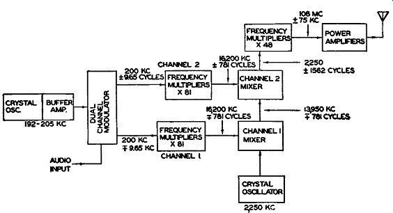
Fig. 16.18A. A block diagram of the dual channel modulator circuit.
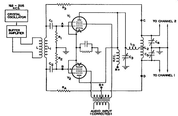
Fig. 16.18B. The modulating circuit of the dual channel FM transmitter.
The basic circuit of the Armstrong Dual Channel Modulator is shown in Fig. 16.18. A crystal oscillator functions at a frequency near 200 khz, the same frequency as in the previous modulator. A buffer stage follows the crystal to serve as an isolation amplifier, improving circuit stability. If desired, the crystal oscillator can be placed in a temperature-controlled oven, although this is not necessary in this system. As we shall see presently, any variations in this oscillator have no effect on the final transmitter frequency.
The output of the buffer amplifier is coupled to the modulator input coil, L1 (see Fig. 16.18B). The voltage appearing across L1 is applied to the balanced modulator--consisting of tubes V1 and V2--and to points C, D. In the modulator stages, the carrier signal is shifted 90° and then audio modulated to produce the upper and lower sidebands. After this, the side bands are recombined with the carrier at points C, D. It is here that the phase modulation (and, with it, of course, the frequency modulation) appears.
Modulator Operation. At the balanced modulator, the signal at L1 is applied to the phase-shifting network, C1R 1 and C2R2. Both capacitors are equal in value, and the same is true of the resistors. At the frequency used by the carrier, the reactances of C1 and C2 arc much greater than the resistance of R1 or R2 . Hence, the current through each branch will be practically 90° ahead in phase, with respect to the voltage across L1. Since the voltages across R1 and R2 are in phase with the current through the resistors, we note that the voltage received by each grid will lead the carrier voltage at L1 by 90°. The required 90° phase shift has thus been acquired. Now to the production of the sidebands.
The grids of V1 and V2 are excited 180° out of phase, whereas their plates are connected across a common load. During those intervals when no audio-modulating voltage is present at the screen grids, no output is produced. Upon the application of an audio voltage, one tube draws more current than the other and sideband voltages appear. These are coupled through C3 and L3 to L2 where the carrier voltage from the modulator input coil is directly applied.
To the carrier voltage arriving from L1, points C and D appear as the terminals of a purely resistive network. L2 in conjunction with C4 and C5 forms a parallel resonant circuit at the carrier frequency of 200 khz. Because of the resistive impedance between points C, D, the carrier voltage here is in phase with the voltage at L1. Resistors R3 and R4 are merely inserted for the purpose of preventing undesirable interaction between the modulator and L2, C4, and C5. The ground connection between C4 and C5 produces equal and opposite carrier frequency voltages for the two separate channels of amplifiers. The equality exists because C4 and C5 are equal in value.
In the circuit, to this point, the 90° -shifted sidebands and the direct carrier (or, at least a portion of it) are at points C and D. To understand how phase modulation is achieved it will be necessary to examine in greater detail the electrical action of L2 , C3 , L3, C4 , and C5 . These components of Fig. 16.18B have been rearranged as shown in Fig. 16.19. In the rearrangement, L2 has been separated into two mutually coupled coils of equal inductance, L2,1 and L2B. Their total inductance is equal to L2.
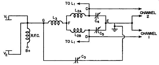
Fig. 16.19. The electrical network wherein the sideband and carrier
voltage combine.
The carrier voltage is brought to points C, D. These two points also lead to the two tripler channels, as can be seen from Fig. 16.18B. Because L2A plus L2B equal L2, and L2C4C5 is resonant to the carrier frequency, then the entire series branch shown in Fig. 16.19, around points C, E, D, and F, is resonant to the carrier frequency.
To the carrier voltage, this network offers maximum impedance because it is connected as a parallel resonant circuit. It is also to be noted that, since both arms of the network (L2A and C4 or L2B and C5 ) are equivalent, each is resonant to the carrier frequency. This leads to the following result: Any voltage placed between points C and D "sees" a parallel resonant circuit.
However, any voltage applied between F and E "sees" two series resonant circuits. This latter fact should be kept in mind while we consider the introduction of the sidebands between points F and E. The sideband voltages are applied from the R.F. choke in the plate circuit of V1 and V 2 to L3C3 and the network within terminals CDEF. L3 in conjunction with Ca resonates at the carrier frequency. The presence of L2A, L2B, C4 and C5 in the resonant network of L3C3 does not produce any interference because a voltage at the carrier frequency applied between F and E "sees" only resistance. Thus, whether we are considering the circuit in Fig. 16.19 from the terminals leading to points C and D or from the terminal leading from the balanced modulator, we have a completely resonant circuit presented to the carrier frequency. This design is purposely effected in order to obtain the correct phase relationships when the side band voltages are applied.
The sideband voltages are applied to this circuit between point G and ground. In the inductive branch of the resonant circuit (the branch containing L3 and the network from point F to ground) the current lags the sideband voltages by 90°. This is true of all inductive branches. The inductive current flows down through La, and, at point F, divides evenly between L2AC4 and L2BC5. Each of these two branches appears resistive to the side band current, since the sideband frequencies are so very close to the carrier frequency.
The sideband currents, in flowing down each branch, develop voltages across C4 and C5 . However, across a capacitor, the voltage lags the current by 90°. Hence, the voltage that appears across C4 and C., is 90° (owing to its flow through La) plus an additional 90° (owing to the voltage and current relationships across a capacitor) out of phase with respect to the sideband voltages applied by the modulator to terminal G and ground.
And, owing to the modulator input network, C1, C2 , R1, and R2 , another 90° shift was introduced. The overall result is this: the sideband voltages appearing across C4 and C5 are 180° + 90°, or 270°, out of phase with the carrier voltages at C4 and C5. But 270° in one direction (say, clockwise) is equal to 90° in the opposite (or counterclockwise) direction. Thus, the sideband frequencies and the carrier are combined 90° out of phase with each other. This is the desired result.
To recapitulate, we have the sideband frequencies formed at V1 and V2 and shifted 90° (by C1, C2, R1, and R2) from the carrier. Then, in the net work composed of C3, L3, L2 , C4 , and C5, the sideband frequencies arc shifted an additional 180°. Since 180° + 90° is equal to 270°, and 270° clockwise is the same as 90° counterclockwise, we find that the sidebands and the carrier are combined 90° out of phase with each other. This produces phase modulation and, with it, equivalent frequency modulation.
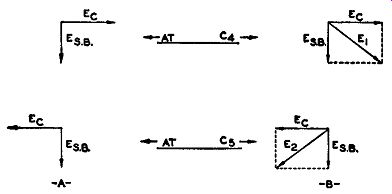
Fig. 16.20. The vectorial addition of the sideband and carrier voltage.
The sideband voltages at C4 and C5 are equal to each other, both in amplitude and phase. We can indicate this fact in Fig. 16.20A by making their vectors equal to each other and pointing in the same direction. To add the carrier voltages to these vectors, we note that across C4 and C5 they arc equal but opposite in polarity. The carrier voltages at C4 and C5 are opposite in polarity because C and D (from whence they are applied) are at opposite ends of the input coil, L1 (see Fig. 16.18B). They differ, in other words, by 180°. This is shown in Fig. 16.20A. Adding the vectors for the sidebands and the carrier voltages, we obtain the result shown in Fig. 16.20B. One resultant vector, E1 , lags its carrier voltage; the other resultant vector, E2, leads its carrier voltage. In terms of equivalent frequency variations, this means that if, in channel No. 1, the frequency swing is +9.65 cycles, then, in channel No. 2, the corresponding frequency swing is -9.65 cycles.
When one frequency swing is positive, the other frequency swing is negative.
Each channel contains four tripler stages, multiplying each signal frequency by 3 x 3 x 3 x 3, or 81. Hence, the input 200 khz, with the associated 9.65-hz frequency swing, becomes at each channel output 16,200 khz.
Each has a frequency variation of 781 cycles. This is shown in Fig. 16.18A. The output of each channel is fed into a separate mixer. Feeding into the first mixer is the voltage from a 2250- khz crystal oscillator and the 16,200 khz,= 781 cycles derived from channel No. 1. As a result of the mixing process, a difference frequency of 13,950 khz ± 781 cycles is produced. This is fed to a second mixer, where it meets the incoming signal from channel No. 2.
We obtain a carrier output from the second mixer of 16,200 - 13,950 khz, or 2250 khz. For the sidebands we have ±781 - ,=781 cycles, or ±781 + ±781 cycles, or ±1562 cycles. Note what has been done here. With the negative or minus sign, we have converted ,=781 cycles to ±781 cycles. Arithmetically and electrically, this is what actually occurs. Hence, we obtain a signal from the second mixer which has twice the frequency swing of either channel.
From here, four doublers and a tripler (providing a multiplication of 2 X 2 X 2 X 2 X 3 = 48) increases 2250 khz ± 1562 cycles to 108 mhz ± 75 khz.
One or more power amplifiers then boost the signal power to its final output value.
In the Armstrong Dual Channel Modulator, the crystal control oscillator feeding the first mixer regulates the stability (and the value) of the final carrier value. In the foregoing illustration, if we desire an output carrier of 90 mhz, the crystal control oscillator would have to be lowered to 1875 khz.
Any other carrier frequency in the band 88 to 108 mhz can be obtained accordingly.
Frequency Stability. The stability of the carrier frequency may be seen indicated by the following example. Assume that the crystal oscillator feeding the modulator unit shifts in frequency by 1 khz, say, from 200 khz to 199 khz. In each channel the incoming 199 khz is multiplied 81 times to a final value of 16,119 khz. If the control oscillator is set at 2250 khz, then the difference frequency output from the first mixer is 13,869 khz. At the second mixer, 13,869 khz and 16,119 khz mix to produce 2250 khz, which is exactly what we wish. The shift from 200 khz to 199 khz had no effect upon the frequency modulation. Hence, no matter to what value the first crystal oscillator changes, the output frequency from the second mixer will be entirely determined by the crystal control oscillator. Actually, all that the two channels and the balanced modulator do in this system is to produce the frequency modulation. The frequency variation is increased 81 times in the channels and then transferred to the control crystal oscillator carrier.
Although it makes no difference what change occurs in the frequency of the first oscillator, too much shifting would tend only to reduce the amplitude of the signal from each channel because of attenuation in the tuned circuits. Hence, it is customary to use a crystal oscillator, although any of the other types of familiar oscillators (Hartley, Colpitts, T.G.T.P., etc.) would be satisfactory.
The phase-shift method of securing frequency modulation produces a signal with very little distortion. It is claimed that the dual-channel principle has even decreased the previously small amount of distortion present.
The measured rms harmonic distortion is less than 1 ½ percent for all audio frequencies between 50 and 15,000 cycles at 25 percent, 50 percent, and 100 percent modulation. This is well within the standards of "Good Engineering Practice" of the F.C.C. as applied to broadcast stations.

Fig. 16.21. The Serrasoid FM modulator.
The Serrasoid FM Modulator. An FM modulator which is capable of securing a relatively large initial phase shift with only four tubes was developed by J. R. Day. The name of this new unit is the Serrasoid FM Modulator. For a modulating frequency of 50 cycles, peak deviations close to ±100 cycles can be obtained. Since an FM carrier is permitted a maximum frequency deviation of ±75 khz, or 75,000 cycles, a fairly high multiplication is required. The figure generally falls between 800 and 1,000, depending on the deviation achieved in the oscillator.
The schematic circuit of the Serrasoid modulator is shown in Fig. 16.21. V1 is a crystal oscillator which j_i_ _ 8 _ generates a frequency having a value of 1/972 of the final carrier frequency.* By placing the crystal in an oven, the frequency generated can be held within ±0.0002 percent of its assigned value, thereby insuring that the final carrier stability is of the same order.
[* This is for the circuit as developed by J. R. Day. In the commercial unit shown in Fig. 16.24, it would be 1/864 of the final carrier frequency.]
The oscillator circuit is so designed that the crystal current is very small, and the tube conducts for only a small fraction of time. The result is that narrow negative-going pulses are produced at the plate of the tube. (See Fig. 16.22A.) These pulses are applied to the grid of V 2 through a differentiating network composed of C1 and R1 which tend to narrow down the pulses still further. At the grid of V 2 the pulses plunge the tube into cut-off producing positive-going pulses with flat tops at the plate. These pulses are applied through C2 to the grid of Va, a cathode follower. Fig.16.22. (A) Voltage waveform at plate of V1 Fig. 16.21. (B) Voltage pulses across R3 of Fig. 16.21.
This tube is biased beyond cut-off by the combination of cathode and grid-leak bias, the latter being developed by the combination of C2 and R2 and the positive pulses which are fed to the tube by V2. Because of its method of biasing, Va clips the bottom of the pulses, producing a pulse across R3 which has steep sides and is fairly square.
(See Fig. 16.22B.)
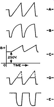
Fig. 16.23. Additional waveforms of Fig. 16.21. (See text for explanation.)
The pulses now are fed to V 4 which is a non oscillating saw-tooth wave generator. Here is how it operates. The grid initially possesses no bias.
Upon the arrival of a positive-going pulse from R3, grid current flows from V4 into Ca, charging this capacitor to essentially the peak value of the applied pulse. During the interval between pulses, C3 discharges slowly through its shunting resistor, R4 , but because of the high value of R4, the voltage across Ca is sufficiently high to keep V4 cut-off except when the pulses are active.
A capacitor, C4, is connected across the output _ circuit of V 4. When the tube is cut-off, the voltage UU-E- across C4 rises because one end of this capacitor is connected through R5 and R6 to the B+ power supply while the other end connects to ground.
C4 continues to charge until a pulse arrives at the grid of V4 , at which time V 4 is driven sharply into conduction. The pulse reduces the internal resistance of V 4 to a low value, and, since V4 is directly across C4 , the capacitor discharges rapidly through this low resistance. At the end of the pulse, V 4 again returns to cut-off, and C4 again starts its charging.
Now, it is most important that the voltage across C4 rise as linearly as possible (Fig. 16.23A) because the linearity of the modulation process depends upon it. Normally, however, the charging of a condenser is not linear but exponential, as shown in Fig. 16.23B. This is so because, as the voltage across a charging capacitor rises, it tends to buck or counteract the applied B+ voltage, reducing the ability of this latter voltage to keep the charging current constant. To insure that the rise will be linear, a "bootstrap" amplifier comprising V5 , C5 , and R7 is added. The grid of V5 is connected directly across C4, so that whatever voltage is present across C4 becomes the grid voltage for V5. During the charging period of C4 , the grid voltage of V5 is rising, causing the current through this tube to increase. This results in a rising voltage across R7. Since C5 is connected between the top of R7 and R5 , the voltage rise across R7 is transferred, via C5 , to the B+ voltage present at point A. Thus the B+ charging voltage for C4 has superimposed on it the rising voltage from R7. (See Fig. 16.23C.) This increase in B+ voltage offsets the voltage rising across C4, keeping the current flowing into C4 constant and producing a linear rise in voltage across this capacitor.
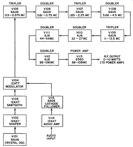
Fig. 16.24. A block diagram of a commercial FM transmitter using the
Serrasoid system. (Courtesy Gates Radio Co.)
C4 is also connected to the grid of V6 , a cathode-biased amplifier. The bias on this tube is so adjusted that conduction begins when the saw-tooth voltage across C has attained only half of its maximum value. (See Fig. 16.23D). 0.25 microsecond after V 6 starts conducting, grid current is drawn, stopping the charging of 0 4 and maintaining its voltage at this value until discharge occurs, after which the process is repeated. The voltage at the plate of V 6 drops abruptly from 250 volts to that corresponding to a fairly low value and remains there until C4 discharges, at which time it rises steeply back to 250 volts because the tube is cut-off. The plate waveform is shown in Fig. 16.23E. Feeding into the cathode of V 6 is the audio-modulating voltage. As this voltage varies, it changes the bias on the tube and, therefore, the time when conduction will begin. When the audio voltage is positive, the start of tube conduction is delayed because a more positive cathode is equivalent to a more negative grid. Conversely, when the audio voltage is negative, tube conduction will commence sooner. This periodic advance and delay of the start of tube conduction causes the leading edge of the plate voltage pulses at the output of V 6 to become phase-modulated. (The end of tube conductions always occurs at the same time since this is controlled by the pulses coming from V3.) Before the audio signal is applied to V 6, it is acted on by a correction circuit (composed of C6 and R10) which counteracts the tendency of the higher audio frequencies to produce more equivalent frequency modulation than the lower frequencies, assuming both signals are equal in strength. This circuit, it will be recalled, is required when frequency modulation is derived from phase modulation, as it is here.
The pulses at the plate of V6 are made narrower by passage through a differentiating network consisting of C7 and R9 and then applied through V7 to a string of doubler and triplers. In the resonant circuits of these multipliers, the pulses are converted to sinusoidal waves possessing the same amount of phase or frequency modulation.
The block and schematic diagrams of a commercial FM transmitter utilizing the Serrasoid method of modulation are shown in Figs. 16.24 and 16.25. After the initial modulated signal is formed by V104 , three triplers and five doublers multiply the signal 864 times to a final carrier value between 88 and 108 mhz with 100% modulation (±75 khz). The signal, at the output of V113, has a maximum average power of 10 watts. This is then raised to the desired final level (250 watts, 100 watts, 5000 watts) by additional power stages.
In spite of the names which this manufacturer has given stages V 101 through V104 , they function in essentially the same manner as V1 through V7 of Fig. 16.21. R16s and 0 11 2 serve the same purpose here as C6 and Rio of Fig. 16.21. That is, they counteract the tendency of the higher audio frequencies to produce more equivalent FM than the lower audio frequencies.
Approximately 30 volts rms of audio is required at the output of the audio amplifier stage, as measured at TP118 , to modulate the FM carrier 100%. Since the audio is applied to the cathode of V 104 , the output impedance of the audio system should be low. For this reason, V 115 is a cathode follower. V114 and V115 work together as a unit since they operate within a feedback loop. The negative feedback is provided by 0 163 and R158, R159 in series. The audio input stage, V 114, is driven by audio input transformer, T102. A suitable pre-emphasis network would be inserted between T102 and the audio input source.
In the frequency multiplier portion of the schematic diagram, V 105 through V112, the circuitry is fairly conventional except in one or two places.
For example, between V105 and V 106 there are three tuned circuits, L101, L102, and L 103 . The purpose of these three circuits is to present to V 106 a sine wave in which every cycle possesses the same amplitude. V105 receives a series of sharp spikes or pulses from V 104. The pulses are being applied at a frequency rate of 116 khz. The plate circuit of V105, consisting of L101 in parallel with a resistor and capacitor, is tuned to three times 116 khz or 348 khz. As each of the sharp spikes occurring at 116 khz arrives at the grid of V105 , the tube suddenly conducts and shocks the plate circuit of V105 into oscillation at its resonant frequency of 348 khz. If an oscilloscope were connected directly to the plate of V 105, these oscillations would appear as shown in Fig. 16.26A.

Fig. 16.26. Waveforms in the circuits between V105 and V106 of Fig.
16.25.
[* This is a representative figure. The actual value would be governed by the assigned carrier frequency of the station.]
These oscillations, it will be noted, are damped. This indicates that the Q of the circuit is fairly low which, in the present instance, is due to the resistor shunted across L101 . If we removed the resistor, the three sine-wave cycles would more closely possess the same amplitude. However, the signal reaching V105 possess a frequency modulation of ±116 cycles. At the output of this tube, the modulation has been increased to ±348 cycles. It is the purpose of the resistor across L101 to broaden the circuit response so that the frequency can be shifted from 348 khz plus 348 cycles to 348 khz minus 348 cycles. Without the loading imposed by the resistor, the Q of the tuned circuit would be high and the flywheel effect of the plate circuit of V10 -- would prevent the circuit from following the frequency excursions faithfully and distortion would result.
The tuned combination of L102 and its shunting capacitor together with
L103 and its shunting capacitor form a bandpass filter that removes the amplitude variation of 116 khz from the 348- khz signal coming from the plate of V105. The grid of V 106 is thereby fed with a pure sine wave of 348 khz. Band width and coupling are determined by the values used for the two coupling capacitors, C118 and C119. If amplitude variations of 116 khz are not removed from the 348- khz signal, the carrier will tend to become phase-modulated at the driving frequency of 116 khz and cause spurious frequencies to appear at the exciter output. The necessary bandwidth of circuitry between V105 and V106 is determined by the highest modulating frequency and the frequency deviation. For the circuits of V105 and V106, this turns out to be 35 khz.
Similar reasoning is behind the selection of the tuning circuits in the remaining stages. In V106 through V112, two coupled tuning circuits provide the necessary bandpass, because, as we go higher in frequency, the necessary bandspread is achieved more readily. That is, if the same Q is maintained, increase in operating frequency results in a proportionately greater band pass.
It will be noted that a short coaxial cable jumper connects V109 and V110. The combination of Lno, C 137, and C 138 tunes the plate circuit of V 109 to the proper resonant frequency. C 137 and C 138 are impedance-transforming capacitors that change the high impedance output of V109 to about 51 ohms at J 101. This makes it possible to carry the output of V109 over a consider able length of coaxial cable to another amplifier stage without serious attenuation. From this external amplifier (not shown), another length of coaxial cable may be brought back to J102. The capacitor combination of C139, C140, and 0 141 then transfers the 51-ohm impedance back to a high impedance in addition to resonating L 111 to the operating frequency.
J101 and J102 are used specifically for the purpose of inserting multiplex sub-carriers on the main carrier, should this be desired. If not, J101 connects directly to J102.
V105 through V109 are single-ended stages and use 6A U6 pentode tubes.
V110 through V112 are push-push stages and all use 6J6 twin triode tubes.
The grids of these push-push stages are connected in normal push-pull fashion, but the plates are connected in parallel. With this type of connection, the plate circuit receives two pulses for every complete cycle of R.F. drive in the grid circuit. This makes it naturally suited to frequency doubling service since the circuit will not amplify a fundamental frequency and will not triple. It will only double or quadruple. The quadruple frequency, however, will be out of the tuning range of the stage.
Before we leave the subject of FM through phase modulation, brief mention should be made of a tube, the Phasitron, which can accomplish this directly. The tube, developed by Dr. Robert Adler of the Zenith Corporation in 1946, utilizes a series of 36 deflection grids, a 3-phase oscillator signal and an external modulating coil to produce an FM signal through phase modulation. The grids, in conjunction with the 3-phase signal, develop the rotating electron disc shown in Fig. Fig. 16.27.
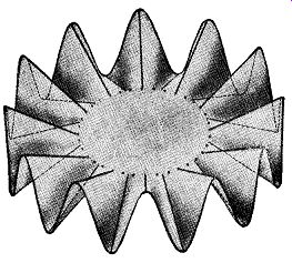
Fig. 16.27 The electron disc developed in the Phasitron tube.
The external modulating coil, through which the audio currents pass, causes the rotating disc to shift back and forth in accordance with the modulating signal. In essence, this is exactly the same action that occurs in the vector diagram used originally to explain phase modulation in section 2.
A small number of FM transmitters were built by General Electric using the Phasitron, but no extensive application ever developed.*
EXAM
1. Name 4 methods of producing phase modulation.
2. Describe how the circuit of Fig. 16.2 produces phase modulation.
3. Draw a diagram of the Gm phase modulator and explain how it operates.
4. Describe the operation of the reactance-tube phase modulator. In what way does this differ from a reactance-tube modulator which produces FM directly?
5. What is the difference between a linear and a nonlinear inductance? What causes the nonlinearity?
6. How does the circuit of Fig. 16.7 A produce phase modulation?
7. What is the Armstrong system of generating frequency modulation? Why is it useful?
8. What factors govern the amount of FM produced through phase modulation? How are these factors combined in a formula?
9. Draw a block diagram of the basic Armstrong system. Explain the function of each stage.
[* Those readers desiring more information about this tube are referred to:
1. Robert Adler, "A X cw System of Frequency Modulation," Proc. of the Institute of Radio Engineers, January, 1947.
2. F. M. Bailey and H. P. Thomas, "Phasitron FM Transmitter," Electronics, October, 1946.]
10. What limitations must be observed when employing phase modulation to produce FM? How docs the Armstrong system observe these limitations?
11. What is a pre-distorter network? Draw a diagram of such a network and connect it to an amplifier.
12. Why is a pre-distorter network required in the Armstrong modulator?
13. When a full phase swing of 30° is utilized, how much equivalent FM is produced when the audio signal frequency is 1000 cycles?
14. Differentiate between pre-distorter networks and accentuator circuits. Where is each used?
15. Why is pre-distorter circuit design based upon the lowest audio frequency used in the modulator?
16. How much frequency multiplication is required in the Armstrong FM transmitter in order to obtain a fully modulated wave? How does this affect the carrier frequency and how is a final carrier value between 88-108 mhz achieved?
17. How docs the Armstrong Dual Channel Modulator differ from the basic circuit?
18. What stage determines the accuracy of the final carrier frequency in the Dual Channel Modulator Transmitter? Explain.
19. Explain by means of a block diagram the operation of the Dual Channel Transmitter.
20. What advantages does the Armstrong Dual Channel Transmitter possess over the basic Armstrong circuit?
21. Discuss the differences between AM and FM transmitters of comparable power. Limit the discussion to audio modulating power required, carrier frequency stability, types of tubes required and overall economy.
22. What docs an FM receiver contain to counteract the effect of the pre-distorter and accentuator networks in the transmitter? Explain your answer in detail.
23. Explain briefly the operation of the Serrasoid FM modulator.
+++++++++++