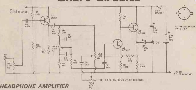
HEADPHONE AMPLIFIER
This simple stereo amplifier will drive a pair of stereo headphones, and can take its input from either a tuner or cassette deck. It has the advantage over a normal stereo amplifier of being small, completely self contained, and therefore very portable. Of course, many tuners and cassette decks have a headphone output, but this often lacks sufficient drive, and there are usually no tone controls (or volume and balance controls in some cases). This circuit gives the usual tone, balance, and volume control facilities, and also has plenty of drive. Ideally the unit should be used with phones having an impedance of a few hundred ohms each, and most good quality types fall into this category, it also seems to work perfectly well with inexpensive 8 ohm types.
The circuit shown here is for one channel, all the components being duplicated in the other channel except for S1, BY1, and. RV4, which are obviously common to both channels. The two RV1s are a dual gang component, as are the two RV2s and the two RV3s.
The input signal is applied to volume control VR1, and from here it is coupled to a buffer stage based on Q1. This gives the unit a reasonably high input impedance of at least 100k. Its output feeds a conventional passive tone control circuit that can give bass lift or cut using RV2, and treble lift or cut using RV3. RV4 is used in the standard balance control arrangement. The output from the tone controls is coupled by C6 to a two stage direct coupled amplifier. This uses Q2 in the common emitter mode to give sufficient voltage gain for an output level of up to about 2 V RMS from most sources. Q3 is an emitter follower buffer stage which matches the output from Q2 to the relatively low impedance of the headphones.
The unit has a total current consumption for both channels of "Z about 30mA.
-----------
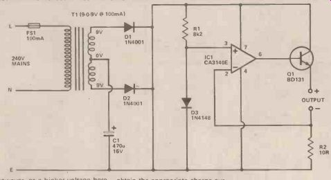
NICAD CHARGER
This charger is intended for use with the popular AA size NiCad batteries (similar to ordinary HP7 cells). A special charger is needed for NiCad calls because they have a very low internal resistance, leading to an excessive charging current even if the applied voltage is only marginally high. The charger must therefore incorporate a circuit to limit the charge current to the appropriate level.
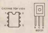
In this circuit, T1, D1, D2, and C1 form a conventional stepdown, isolation, fullwave rectifier, and smoothing circuit. The other components provide the current regulation. IC1 is used as a comparator with discrete buffer stage Q1 giving a suitably high output current capability for this application. IC1's non-inverting input is fed with a 0.65 V. reference potential provided by R1 and D3.
The inverting input is taken to earth by R2 under quiescent conditions, causing the output to go fully positive. With a NiCad cell connected across the output a high current will attempt to flow, causing the voltage across R2 to Increase. It can only rise to 0.65V. E however, as a higher voltage here reverses the comparative input levels to IC1, resulting in the output going lower in voltage, and reducing the voltage across R2 back 0.65 V. The maximum output current (and the charge current obtained) is therefore the current produced with 0.65 V. across 10 ohms, or 65 mA. in other words.
Some AA NiCad cells have a maximum recommended charge current of only about 45 or 50 mA, and for these types R2 should be increased to 13 ohms in order to obtain the appropriate charge current. Some rapid charge types will take 150 mA, and this necessitates reducing R2 to 4.3 ohms (3.3 ohms plus 1 ohm in series if a suitable component cannot be obtained). Also, T1 should be changed to a type having a current rating of 250 mA., and C11 should be fitted with a small bolt-on finned heatsink. The unit can charge up to four cells (six if T1 is made a 12 V type), and these must be connected in series across the output, not in parallel.
-----------------
SUSTAIN UNIT
Normally each note from a guitar has a high initial volume that rapidly decays to a much lower level, and the gradually fades out.
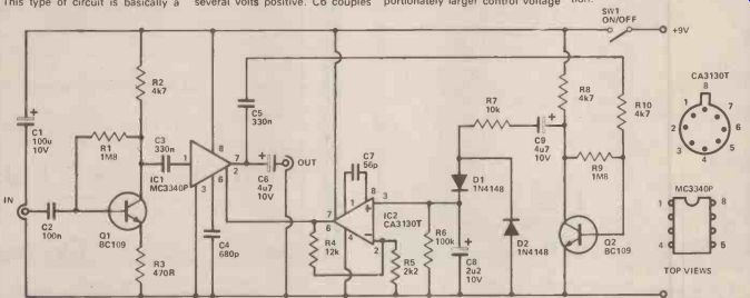
A sustain unit provides a relatively constant output level when used with an electric guitar, despite the wide range of input levels. The most simple form of sustain unit is a clipping amplifier, but these inevitably introduce quite large amounts of distortion. A better method, and the one used in this unit, is to use a compression circuit having fast attack and decay times.
This type of circuit is basically a voltage controlled amplifier, the gain of the circuit being controlled by an output level sensing circuit which varies the gain to produce a fairly consistent output level. Little distortion is produced using this method.
Q1 is used as a low noise pre amplifier having a voltage gain of about 20 dB. Its output is fed by C3 to the input of IC1, the voltage controlled amplifier device. This has a quiescent voltage gain of about 1 3dB, but this can be reduced to an attenuation of over 70 dB by taking pin 2 of the device several volts positive. C6 couples some of the output from IC1 to the output socket, and C5 couples the remaining output to a common m emitter amplifier based on Q2. The amplified signal at Q2 collector couples via C9 and R7 to a conventional smoothing and rectifier network. The positive bias produced by this network is fed to the control input of IC1 via a low gain amplifier and buffer stage based on IC2.
With 16w input levels (below about 1mV) the control signal is too small to affect the gain of IC1 Higher level signals produce a proportionately larger control voltage and lower gain through IC1, preventing the output level from rising much above about 30mV RMS, and giving the required virtually constant output level. The attack and decay times of the circuit are both quite short so that the unit responds suitably rapidly to changes in input level, but neither of these time constants are so short .1" as to cause serious distortion. The unit will be most effective with the volume control on the guitar set at maximum, unless the output should then be so high as to overload the unit and cause distortion.
------------
AC METER BOOSTER
Measuring small audio 'frequency signals is often impossible using an ordinary multimeter because most of these have a lowest AC range of about 1 to 5 V FSD. A simple and inexpensive solution to the problem is to add an amplifier, such as the one shown here, ahead of the multimeter. The amplifier has a switched voltage gain of 10 or 100, and would therefore boost the sensitivity of ksay) a multimeter switched to the 2.5 V AC range to 250 mV and 25 mV FSD respectively. Measurements down to just a few mV RMS can then be made with reasonable accuracy.
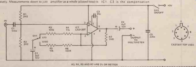
The circuit uses a CA3 1 30T operational amplifier in the non-inverting mode. The non-inverting input is biased to about half the supply voltage by R1 and R2, and he input signal is coupled to this point by C1. The input impedance of the circuit is set at over 1M by A1 and R2, so that the unit places little loading on the circuit under est. R7 biases the inverting input and gives a quiescent output voltage of about half the supply potential. Although IC1 has an extremely high open loop) voltage gain, the voltage gain of the amplifier as a whole (closed loop) is much lower, and is set by the ratio of two resistances. With SW1 in the 'X 10' position the two resistances are R7, and R3 plus R4. The voltage gain is equal to the sum of the two resistances divided by the shunt resistance (R3 + R4) in this negative feedback network. This gives almost exactly the required figure of 10 with the specified values. With SW1 in the 'X 1 0 0' position the lower shunt resistance of R5 and R6 is switched into circuit, boosting the voltage gain to almost exactly 100.
DC blocking at the output is provided by C4. C5 is a supply decoupling capacitor and should be mounted physically close to IC 1 C3 is the compensation capacitor for IC1, and prevents the device from becoming unstable.
Note that a carefully designed layout having the input and output well isolated from one another is required, or the circuit as a whole may become unstable. Screened input and output cables should be used to drive the primary winding maximum output of about 3 V RMS. It should therefore be used with the multimeter set to a range of 3 V or less, or if a higher range must be used, the part of the scale above 3 V is ignored. The amplifier has a flat response up to about 30kHz in the 'x100' mode, and up to about 300kHz in the 'x10' mode.
-----------
ZENER DIODE TESTER
This circuit is an add-on unit for a multimeter having a sensitivity of 20k/V or better, and it enables a rough check to be made on zener diodes having operating voltages of up to about 33 volts. The unit operates from a standard 9 volt battery (PP6, PP7, or PP9 size), no mains supply or special, high voltage battery being required.
In order to obtain a suitably high voltage for this application from an ordinary 9 volt DC supply it is necessary to have a voltage step up circuit of some kind. In this case an audio oscillator using IC1 is used to drive the primary winding of step-up transformer T1, giving about 50 V AC from the secondary winding. T1 is actually intended for use as a step-down transformer in transistor amplifier output stages, but it provides satisfactory results when employed in reverse to give a voltage step-up. The output from T1 is halfwave rectified and smoothed by D1 and C3 to give to give an unloaded DC supply of about 75 to 80 volts (about 40 to 50 V when loaded).
With SW1 at the low position, a current of about 1 to 2 mA, (depending upon the voltage of the zener under test) is fed to the test device through current limiting resistor R4, when W2 is operated and power is applied to the circuit.
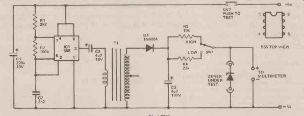
The multimeter, which is switched to an appropriate DC voltage range, is connected in parallel with the test device and registers its zener voltage. Switching SW1 to the 'high' position causes about double the previous current to flow through the zener under test, as a lower value current limiting resistor (R3) is then switched into circuit. If the test device is fully functional this should cause only a very small increase in the meter reading, and there may well be no noticeable change in the meter reading at all.
---------
(adapted from: Hobby Electronics magazine, Sept. 1979)
Also see:
Thyristors: The Great Gate Story
FET--Special Down the Gain Drain