THE SUPERHET SYSTEM
It will have been appreciated from the above that any multiple tuned circuit, or SAW filter, system chosen to give good selectivity will be optimized only for one frequency. To tune a group of critically coupled bandpass tuned circuits simultaneously to cover a required receiver frequency range would be very difficult. To tune one or more SAW filters simultaneously would simply not be possible at all, except, perhaps, over an exceedingly limited frequency range.
A practical solution to this problem was offered in 1918 by Major Armstrong of the US Army, in the form of the supersonic heterodyne or superhet receiver system, shown in FIG. 21.
In this, the incoming radio signal is combined with an adjustable frequency local oscillator signal in some element having a non-linear input/output transfer characteristic, (ideally one having a square-law slope). This stage is known as the frequency changer or mixer or, sometimes, and inappropriately, as the first detector.
This mixture of the two (input and LO) signals gives rise to additional sum and difference frequency outputs, and if the local oscillator frequency is chosen correctly, one or other of these can be made to coincide with the fixed intermediate frequency (usually known as the IF), at which the bulk of the amplification will occur.
The advantages of this arrangement, in allowing the designer to tailor his selectivity characteristics without regard to the input frequency, are enormous, and virtually all commercial radio receivers employ one or other of the possible permutations of this system.
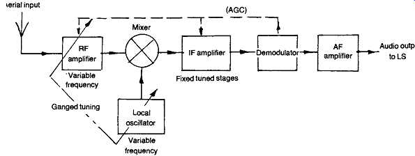
FIG. 21 The superhet system.
PROBLEM
The snag is that the non-linear mixer stage produces both sum and difference frequency outputs, so that , for any given local oscillator frequency there will be two incoming signal frequencies at which reception would be possible.
These are known as signal and image frequencies, and it’s essential that the selectivity of the tuned circuits preceding the mixer stage is adequate to reject these spurious second channel or image frequency signals. This can be difficult if the IF frequency is too low in relation to the incoming signal frequency, since the image frequency will occur at twice the IF frequency removed from the signal, which may not be a very large proportion of the input signal frequency, bearing in mind the selectivity limitations of conventional RF tuned circuits.
In communications receivers and similar high-quality professional systems, the problem of image breakthrough is solved by the use of the double superhet system shown in FIG. 22. In this the incoming signal frequency is changed twice, firstly to a value which is sufficiently high to allow complete elimination of any spurious image frequency signals, and then, at a later stage, to a lower frequency at which bandwidth limitation and filtering can be done more easily.
A difficulty inherent in the superhet is that, because the mixer stage is, by definition, non-linear in its characteristics, it can cause intermodulation products between incoming signals to be generated, which will be amplified by the IF stages if they are at IF frequency, or will simply be combined with the incoming signal if they are large enough to drive the input of the mixer into overload.
This type of problem is lessened if the mixer device has a true square law characteristic. Junction FETs have the best performance in this respect.
A further problem is that the mixer stages tend to introduce a larger amount of noise into the signal chain than the other, more linear, gain stages, and this may well limit the ultimate sensitivity of the system. The noise figure of the mixer stage is partly a function of the kind of device or circuit configuration employed, and partly due to noise introduced by the relatively large amplitude local oscillator signal.
It’s undoubtedly true to say that the quality and care in design of the mixer stage from a major determining factor in receiver performance, in respect of S/N ratio and freedom from spurious signals.
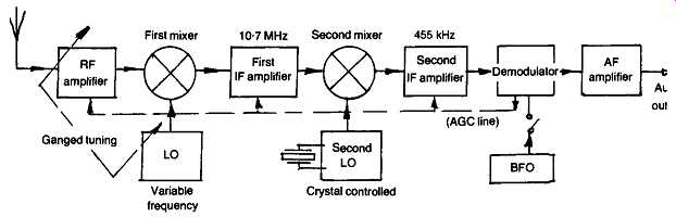
FIG. 22 The double-superhet system, as used in a communication receiver.
OTHER POSSIBILITIES
Because of the problems of the superhet system, in respect of mixer noise, and image channel interference, direct conversion systems have been proposed, in which the signal is demodulated by an electronic switch operated by a control waveform which is synchronous in frequency and phase with the input signal. These are known as homodyne or synchrodyne receivers, depending on whether the control waveform is derived from the carrier of the incoming signal or from a separate synchronous oscillator.
Since both of these systems result in an audio signal in which adjacent channel transmissions are reproduced at audio frequencies dependent on the difference of the incoming signal from the control frequency, they offer a means for the control of selectivity, with a truly flat-topped frequency response, by means of post-demodulator AF filtering. On the debit side, neither of these offer the sensitivity or the ease of operation of the conventional superhet, and are not used commercially to any significant extent.
Sensitivity
Many factors influence this characteristic. The most important of these are:
• the S/N ratio, as depending on the design, small signals can get buried in mixer or other circuit noise;
• inadequate detectability, due to insufficient gain preceding the demodulator stage;
• intermodulation effects in which, due to poor RF selectivity or unsatisfactory mixer characteristics, the wanted signal is swamped by more powerful signals on adjacent channels.
The ultimate limitation on sensitivity will be imposed by aerial noise, due either to man-made interference, (RFI), or to the thermal radio emission background of free space. The only help in this case is a better aerial design.
As mentioned above, the frequency changer stage in a superhet is a weak link in the receiver chain, as it introduces a disproportionately high amount of noise, and is prone to intermodulation effects if the signals present exceed its optimum input signal levels.
The problem of mixer noise is a major one with equipment using thermionic valves, but semiconductor devices offer substantial improvements in this respect. For professional equipment, diode ring balanced modulator layouts, using hot carrier or Schottky diodes, of the kind shown in FIG. 23, are the preferred choice, since they combine excellent noise characteristics with the best possible overload margin.
However, this is a complex system.
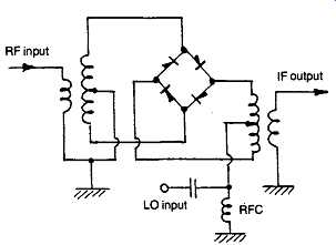
FIG. 23 Diode ring double balanced mixer system.
In domestic equipment, at frequencies up to about 100 MHz, junction FETs are the preferred devices, though they have inconveniently large inter-electrode capacitances for RF use. In the frequency range 100-500 MHz, dual-gate MOSFETs are preferable because their form of construction allows very good input - output screening, though their noise figure and other characteristics are somewhat less good than those of junction FETs.
Beyond 500 MHz, bipolar junction transistors are the only practical choice, though their use demands careful circuit design.
Integrated circuit balanced modulator systems have attracted some interest for high-quality designs, and have even been proposed as an alternative to ring diode modulators, though they have relatively poor overload characteristics. The various practical mixer systems are examined later, under 'Circuit design'. In general, the best performance in a receiver, in respect of S/N ratio, sensitivity, and overload characteristics, requires a careful balance between the gain and selectivity of the various amplifying and mixing stages.
Stability
In a superhet system, in which there are a series of selective fixed frequency amplifier stages, the major problems of frequency stability center around the performance of the local (heterodyne) oscillator, which is combined with the incoming signal to give IF frequency. In relatively narrow bandwidth AM receivers, especially those operating in the short wave (3-30 MHz) region, a simple valve or transistor oscillator is unlikely to be adequately stable, unless very good quality components, and carefully balanced thermal compensation is employed.
Various techniques have been used to overcome this difficulty. For fixed frequency reception, oscillators based on individual quartz crystal or SAW resonators - which give an extremely stable output frequency, combined with high purity and low associated noise - are an excellent solution, though expensive if many reception frequencies are required.
Alternatively, various ways of taking advantage of the excellent stability of the quartz crystal oscillator, while still allowing frequency variability, have been proposed, such as the phase-locked loop (PLL) frequency synthesizer, or the Barlow-Wadley loop systems.
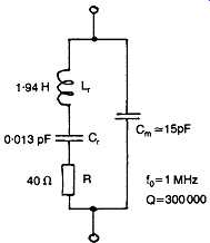
FIG. 24 Equivalent electrical circuit of a quartz crystal resonator.
QUARTZ CRYSTAL CONTROL
This operates by exciting a mechanical oscillation in a precisely dimensioned slab of mono-crystalline silica, either naturally occurring, as quartz, or, more commonly synthetically grown from an aqueous solution under conditions of very high temperature and pressure.
Since quartz exhibits piezo-electric characteristics, an applied alternating voltage at the correct frequency will cause the quartz slab to 'ring' in a manner analogous to that of a slab or rod of metal struck by a hammer.
However, in the case of the crystal oscillator, electronic means can be used to sustain the oscillation.
The monotonic frequency characteristics of the quartz crystal resonator derive from its very high effective Q value. Typical apparent values of Lr, Cr and Cm (the resonant inductance and capacitance, and that due to the mounting), and series loss resistance Ru for an 'X' cut crystal, are shown in the equivalent circuit of FIG. 24 , for a crystal having a resonant frequency of 1 MHz, and an effective ß, as a series resonant circuit, of 300000.
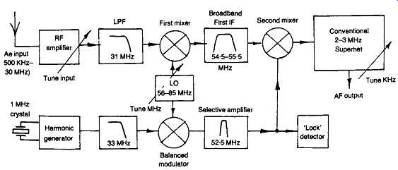
FIG. 25 The Barlow-Wadley loop.
As in other materials, the physical dimensions of quartz crystals will change with temperature, but since its expansion is anisotropy (greater in some dimensions than others) it’s possible to choose a particular section, or 'cut', through the crystal to minimize the effects of temperature on resonant frequency. Such crystals are known as zero temperature coefficient (ZTC) or AT cut types.
Zero temperature coefficient crystals (in practice this will imply temperature coefficients of less than ±2 parts per million per degree centigrade over the temperature range 5-45° C) don’t offer quite such high Q values as those optimized for this quality, so external temperature stabilization circuits (known as crystal ovens) are sometimes used in critical applications. Both of these approaches may also be used, simultaneously, where very high stability is required.
Although, in principle, the quartz crystal is a fixed frequency device, it’s possible to vary the resonant frequency by a small amount by altering the value of an externally connected parallel capacitor. This would be quite insufficient as a receiver tuning means, so other techniques have been evolved.
THE BARLOW-WADLEY LOOP
This circuit arrangement, also known as a drift cancelling oscillator, has been used for many years in relatively inexpensive amateur communications receivers, such as the Yaesu Musen FRG-7, and the layout adopted for such a 500 kHz-30 MHz receiver is shown in FIG. 25.
In this, the incoming signal, after appropriate RF amplification and pre-selection, is passed though a steep-cut, low-pass filter, which removes all signals above 31 MHz, to the first mixer stage. This has a conventional L-C type tuned oscillator whose operating frequency gives a first IF output in the range 54.5-55.5 MHz, which is fed to a second mixer stage.
The L-C oscillator output is also fed to a double-balanced modulator where it’s combined with the output from 1 MHz quartz-crystal controlled harmonic generator, and this composite output is taken through a selective amplifier having a center frequency of 52.5 MHz, and a signal output detector system.
Certain combinations of the local oscillator frequency and the harmonics of 1 MHz will be within the required frequency range, and will therefore pass through this amplifier. When such a condition exists, the output voltage operates an indicator to show that this signal is present. This output signal is then fed to the second mixer stage to generate a second IF frequency in the range 2-3 MHz, from which the desired signal is selected by a conventional superhet receiver from the 1 MHz slab of signals presented to it.
The frequency drift in the first, high-frequency, L-C local oscillator is thereby cancelled, since it will appear, simultaneously, and in the same sense, at both the first and second mixers.
FREQUENCY SYNTHESIZER TECHNIQUES
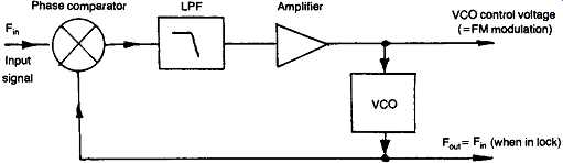
FIG. 26 The phase-locked loop (PLL).
These are based on developments of the phase-locked loop (PLL) shown in FIG. 26. In this arrangement an input AC signal is compared in phase with the output from a voltage controlled oscillator (VCO). The output from the phase comparator will be the sum and difference frequencies of the input and VCO signals.
Where the difference frequency is low enough to pass the low-pass 'loop filter', the resultant control voltage applied to the VCO will tend to pull it into frequency synchronism, and phase quadrature, with the incoming signal - as long as the loop gain is high enough. In this condition, the loop is said to be 'locked'. This circuit can be used to generate an AC signal in frequency synchronism with, but much larger in amplitude than, the incoming reference signal. It can also generate an oscillator control voltage which will accurately follow incoming variations in input signal frequency when the loop is in lock, and this provides an excellent method of extracting the modulation from an FM signal.
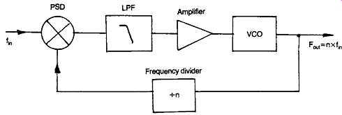
FIG. 27 Phase-locked frequency multiplier.
A further development of the basic PLL circuit is shown in FIG. 27.
In this, a frequency divider is interposed between the VCO and the phase comparator, so that when the loop is in lock, the VCO output frequency will be a multiple of the incoming frequency. For example, if the divider has a factor n, then the VCO will have an output frequency equal to n (Fin). In the PLL frequency synthesizer shown in FIG. 28, this process is taken one stage further, with a crystal controlled oscillator as the reference source, feeding the phase detector through a further frequency divider. If the two dividers have ratios of m and n, then when the loop is in lock, the output frequency will be (n/m) x Fref.
Provided that m and n are sufficiently large, the VCO output can be held to the chosen frequency, with crystal-controlled stability, and with any degree of precision required. Now that such frequency synthesizer circuitry is available in single IC form, this type of frequency control is beginning to appear in high quality FM tuners, as well as in communications receivers.
A minor operating snag with this type of system is that, because of the presence within the synthesizer IC of very many, relatively large amplitude, switching waveforms, covering a wide spectrum of frequencies, such receivers tend to be plagued by a multitude of minor tuning whistles, from which conventional single tuned oscillator systems are free. Very thorough screening of the synthesizer chip is necessary to keep these spurious signals down to an unobtrusive level.
Generally, in FM tuners, the relatively wide reception bandwidth makes oscillator frequency drift a less acute problem than in the case of AM receivers operating at comparable signal frequencies, although, since the distortion of the received signals will in most cases deteriorate if the set is not correctly tuned, or if it drifts off tune during use, there is still an incentive, in high-quality tuners, to employ quartz crystal stabilized oscillator systems.
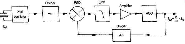
FIG. 28 Phase-locked frequency synthesizer.
A more serious problem, even in wide bandwidth FM tuners -- where these don’t employ PLL frequency control -- is that the varicap diodes (semiconductor junction diodes in which the effective capacitance is an inverse function of the applied reverse voltage) often used to tune the RF and oscillator circuits, are quite strongly temperature dependant in their characteristics.
Varicap-tuned receivers must therefore employ thermally compensated DC voltage sources for their tuning controls if drift due to this cause is to be avoided.
AGC EFFECTS
A particular problem which can occur in any system in which automatic gain control (AGC) is used, is that the operation of the AGC circuit may cause a sympathetic drift in tuned frequency.
This arises because the AGC system operates by extracting a DC voltage which is directly related to the signal strength, at some point in the receiver where this voltage will be of adequate size. This voltage is then used to control the gain of preceding RF or IF amplifier stages so that the output of the amplifier remains substantially constant. This is usually done by applying the control voltage to one or other of the electrodes of the amplifying device so that its gain characteristics are modified.
Unfortunately, the application of a gain control voltage to any active device usually results in changes to the input, output, or internal feedback capacitances of the device, which can affect the resonant frequency of any tuned circuits attached to it. This effect can be minimized by care in the circuit design.
A different type of problem concerns the time-constants employed in the system. For effective response to rapid changes in the signal strength of the incoming signal, the integrating time constant of the system should be as short as practicable. However, if there is too little constraint on the speed of response of the AGC system, it may interpret a low-frequency modulation of the carrier, as For example in an organ pedal note, as a fluctuation in the received signal strength, and respond accordingly by increasing or decreasing the receiver gain to smooth this fluctuation out.
In general, a compromise is attempted between the speed of the AGC response, and the lowest anticipated modulation frequency which the receiver is expected to reproduce, usually set at 30 Hz in good quality receivers. In transistor portable radios, where the small LS units seldom reproduce tones below some 200-250 Hz, a much more rapid speed of response is usable without audible tonal penalties.
Sadly, some broadcasting authorities take advantage of the rapid AGC response typically found in transistor portables to employ a measure of companding (tonal range compression on transmission followed by expansion on reception to restore the original dynamic range). As racticed by the BBC on its Radio 1, Radio 2, Radio 4 and some local radio transmissions, this consists of a reduction in both carrier strength and modulation on all dynamic peaks. This reduces the amount of electricity consumed by the transmitter, whose average power output decreases on sound level peaks.
If, then, the AGC system in the radio restores the received carrier level to a constant value, the original modulation range will be recovered. This will only work well if the AGC 'attack' and 'decay' time constants used in the receiver are correctly related to those employed at the transmitter -- and this is purely a matter of chance. The result, therefore, is an additional and unexpected source of degradation of the broadcast quality of these signals.
AUTOMATIC FREQUENCY CONTROL (AFC)
Because of the shape of the output voltage versus input frequency relationship, at the output of the demodulator of an FM receiver, shown in idealized form in FIG. 29, the possibility exists that this voltage, when averaged so that it’s just a DC signal, with no carrier modulation, can be used to control the operating frequency of the oscillator, or other tuned circuits. So if the tuning of the receiver drifts away from the ideal mid-point (Ft in FIG. 29) an automatic correction can be applied to restore it to the desired value.
This technique is widely used, especially in the case of receivers where the tuning is performed by the application of a voltage to one or more varicap diodes, and which, in consequence, lends itself well to the super imposition of an additional AFC voltage. It does, however, have snags.
The first of these is that there is a close similarity in the action of an AFC voltage in an FM tuner to the action of an automatic gain control in an AM one. In both cases the control system sees the change - in carrier frequency in the case of an FM tuner - which is produced by the program modulation, as being an error of the type which the control system is designed to correct. Too effective an AFC system can therefore lead to a worsening of bass response in the tuner, unless very heavy damping of the response is incorporated.
In the case of FM tuners, it’s likely that the changes to be corrected will mainly be slow, and due only to thermal effects, provided that the receiver was correctly tuned in the first place, whereas in an AM radio the changes in received signal strength can often be quite rapid.
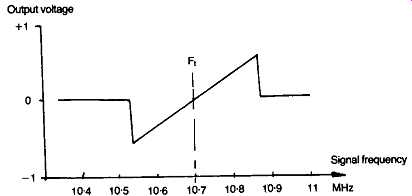
FIG. 29 Voltage/frequency relationships in an ideal FM demodulator.
The second problem is that the AFC system, attempting to sit the tuning point on the zero DC level, may not lead to the best results if the demodulator circuit is misaligned, and gives the kind of curve shown in FIG. 30. Here the user might place the tuning at the point F by ear, where the AFC signal will always restore it to F_t.
This kind of demodulator misalignment is all too common in practice, and is one of the reasons why very linear demodulators (in which the choice of the correct point is less critical) are a worthwhile pursuit. Some more recent systems employ demodulator circuits which are comparatively insensitive to detuning. It should be remembered, also, that the output from the demodulator is likely to be used to operate the tuning meter, and encourage the user to tune to F_t.
In the case of this kind of tuning meter, the user can carry out a quick check on the alignment of the tuned circuits by noting the maximum meter deflection on either side of the incoming signal frequency. These readings should be symmetrical.
Predictability
The possession of a good, clear, tuning scale has always been a desirable virtue in any radio receiver, so that the user could know the point of tune and return without difficulty to the same place. However, with contemporary IC technology, the cost of integrated circuit frequency counter systems has become so low, relative to the other costs of the design, that almost all modern tuners now employ some kind of frequency meter display.
This operates in the manner shown in FIG. 31. In this, a quartz crystal controlled oscillator, operating perhaps at 32.768 kHz, (the standard frequency for 'quartz' watches , for which cheap crystals and simple frequency dividers are readily available - 32768 is 215 ) is used to generate a precise time interval, say one second.
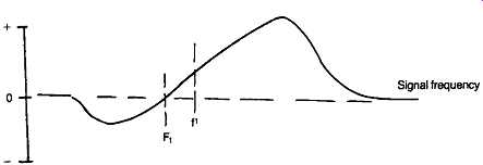
FIG. 30 Effect of demodulator misalignment on AFC operation.
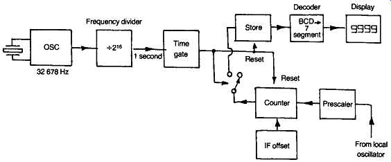
FIG. 31 Frequency meter system.
Meanwhile, the signal from the oscillator of the receiver, which will invariably employ a superhet layout, will be clocked over this period by an electronic counter, in which the IF frequency (that frequency by which the local oscillator differs from the incoming RF signal) will be added to, or subtracted from, the oscillator frequency - depending on whether the oscillator frequency is higher or lower than that of the signal - so that the counter effectively registers the incoming signal frequency.
The electronic switch circuitry operated by the time interval generator is then used alternately to reset the frequency counter to zero, and to transfer its final count to a digital frequency store. A liquid crystal (LCD) or light-emitting diode (LED) display can then be used to register the signal frequency in numerical form.
As a matter of convenience, to avoid display flicker the counter output will be held in a store or latch circuit during the counting period, and the contents of the store only updated each time the count is completed.
Since frequency dither is only likely to affect the last number in the display, in circumstances where there is an uncertainty of ±1 digit, some systems actually count to a larger number than is displayed, or up-date the last - least significant - digit less frequently than the others.
Additional information can also be shown on such an LED/LCD display, such as the band setting of the receiver, whether it’s on AM or FM, whether AFC or stereo decoding has been selected, or the time. In the light of the continual search for marketable improvements, it seems probable that such displays will soon also include a precise time signal derived from one or other of the time code transmitters.
Clarity
One of the major advantages of FM radio is its ability to reject external radio frequency noise - such as that due to thunderstorms, which is very prominent on LF radio, or motor car ignition noise, which is a nuisance on all HF and VHF transmissions, which includes Band 2.
This ability to reject such noise depends on the fact that most impulse noise is primarily amplitude modulated, so that, while it will extend over a very wide frequency range, its instantaneous frequency distribution is constant. The design of the FM receiver is chosen, deliberately, so that the demodulator system is insensitive to AM inputs, and this AM rejection quality is enhanced by the use of amplitude limiting stages prior to the demodulator.
A valuable ' figure of merit' in an FM receiver is its AM rejection ratio, and a well-designed receiver should offer at least 60 dB (1000:1). Because FM receivers are invariably designed so that there is an excess of gain in the RF and IF stages, so that every signal received which is above the detection threshold will be presented to the demodulator as an amplitude limited HF square wave, it’s very seldom that such receivers - other than very exotic and high-cost designs -- will employ AGC, and only then in the pre-mixer RF stage(s). A further benefit in well-designed FM receivers is that intruding AM radio signals on the same band will be ignored, as will less strong FM broadcasts on the same channel frequency. This latter quality is referred to as the capture ratio, and is expressed as the difference in the (voltage) signal strength, in dB, between a more powerful and a less powerful FM transmission, on the same frequency allocation, which is necessary for the weaker transmission to be ignored.
The capture ratio of an FM receiver - a desirable feature which does not exist in AM reception - depends on the linearity, both in phase and amplitude, of the RF and IF stages prior to limiting, and also, to a great extent, on the type of demodulator employed. The best current designs offer 1 dB discrimination. Less good designs may only offer 3-4 dB. Two decibels is regarded as an acceptable figure for high-quality systems, and would imply that the designers had exercised suitable care.
It should be noted in this context that designs in which very high IF gain is employed to improve receiver sensitivity may, by causing overload in these stages, and consequent cross-modulation i f they don’t 'clip' cleanly, lead to a degradation in capture ratio.
Needless to say, those IF stages which are designed to limit the amplitude of the incoming signal should be designed so that they don’t generate inter-modulation products. However, these invariably take the form of highly developed IC designs, based on circuit layouts of the form shown in FIG. 32, using a sequence of symmetrically driven, emitter-coupled 'long-tailed pairs', chosen to operate under conditions where clean and balanced signal clipping will occur.
FM tuner designers very seldom feel inspired to attempt to better their performance by the use of alternative layouts.
In AM receivers, the best that can be done to limit impulse type interference is to use some form of impulse amplitude limiter, which operates either on the detection of the peak amplitude of the incoming signal or on the rate-of-change of that amplitude, such qualities will be higher on impulse noise than on normal program content. An excellent AM noise limiter circuit from Philips, which incorporates an electronic delay line to allow the noise limiter to operate before the noise pulse arrives, is shown in FIG. 33.
The rejection of intruding signals in AM depends entirely on the receiver selectivity, its freedom from intermodulation defects, and - in respect of its ability to avoid internally generated hum, noise, and mush - on the quality of the circuit design and components used, and the wisdom of the choice of distribution of the gain and selectivity within the RF and IF stages.
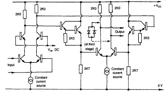
FIG. 32 Cascode input stage, and the first (of two) symmetrical gain stages
in a modern FM IF gain block IC (RCA CA3189E).
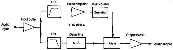
FIG. 33 Philips' impulse noise limiting circuit.
Linearity, FM systems
In view of the continuing search for improved audio amplifier quality in both quantitative and subjective terms, it’s not surprising that there has been a comparable effort to obtain a high performance in FM receiver systems.
This endeavor is maintained by competitive rivalry and commercial pressures, and has resulted in many cases in the development of FM tuners with a quality which exceeds that of the incoming signal presented to them by the broadcasting authorities. Broadcasters' activities are not the subject of competitive pressures, and their standards are determined by the reluctance of governments to spend money on luxuries, and by the cynicism of their engineers.
These constraints have resulted in a continuing erosion of the quality of AM radio broadcasts, though there still remain some honorable exceptions. This has, sadly, often led to the AM sections of FM tuners being designed as low-cost functional appendages having a very poor audio performance, even when the quality of the FM section is beyond reproach.
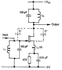
FIG. 34 Feedback neutralization system for junction FET RF amplifier.
A number of factors influence the quality of the demodulated signal, beginning with the stability and phase linearity of the RF, IF and AF gain stages. In the case of AM radios, incipient instability in the RF or IF stages will lead to substantial amplitude distortion effects, with consequent proneness to intermodulation defects. (Any non-linearity in an amplifier will lead to a muddling of the signals presented to it.) In the case of those FM radios based on a phase-sensitive demodulator, any RF or IF instability will lead to substantial phase distortions as the signal passes through the frequency of incipient oscillation.
Much care is therefore needed in the design of such stages to ensure their stable operation. If junction FETs are employed rather than dual gate MOSFETs, some technique, such as that shown in FIG. 34, must be used to neutralize the residual drain-gate capacitance. The circuit of FIG. 34 utilizes a small inductance in the source lead, which could be simply a lengthy track on the printed circuit board, to ensure that the unwanted feedback signal due to the gate-drain capacitance (C) , is can celled by a signal, effectively in phase opposition, due to the drain-source capacitance (C"). However, assuming competent RF/IF stage design, the dominant factor in recovered signal quality is that of the demodulator design. Representative demodulator systems , for FM and for AM, are shown below.
SLOPE DETECTION
This circuit, shown in FIG. 35(a), is the earliest and crudest method of detecting or demodulating an FM signal. The receiver is simply tuned to one side or the other of the tuned circuit resonant frequency (F0), as illustrated in FIG. 35(b). Variations in the incoming frequency will then produce changes in the output voltage of the receiver, which can be treated as a simple AM signal. This offers no AM rejection ability, and is very non-linear in its audio response, due to the shape of the resonance curve.
THE ROUND-TRAVIS DETECTOR
This arrangement, shown in FIG. 36(a), employs a pair of tuned circuits with associated diode rectifiers ('detectors') which are tuned, respectively, above and below the incoming signal frequency, giving a balanced slope detector characteristic, as seen in FIG. 36(b). This is more linear than the simple slope-detector circuit, but still gives no worthwhile AM rejection.
THE FOSTER-SEELEY OR PHASE DETECTOR
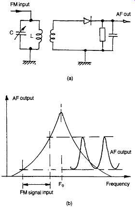
FIG. 35 FM slope detector.
This circuit, of which one form is shown in FIG. 37(a), was evolved to provide an improved measure of AM rejection, by making its output dependent, at least in part, on the changes in phase induced in a tuned circuit by variations in the frequency of the incoming signal.
In this arrangement the tuned circuit, L3Cj, provides a balanced drive to a matched pair of diode rectifiers (D1 , D2), arranged in opposition so that any normal AM effects will cancel out. A subsidiary coil, L2, is then arranged to feed the center tap of L3, so that the induced signal in L2, which will vary in phase with frequency, will either reinforce or lessen the voltages induced in each half of L3, by effectively disturbing the position of the electrical center tap.
This gives the sort of response curve shown in FIG. 37(b) which has better linearity than its predecessors.
THE RATIO DETECTOR
This circuit, of which one form is shown in FIG. 38(a) is similar to the Foster-Seeley arrangement, except that the diode rectifiers are connected so that they produce an output voltage which is opposed, and balanced across the load. The output response, shown in FIG. 38(b), is very similar to that of the Foster-Seeley circuit, but it has a greatly improved AM rejection.
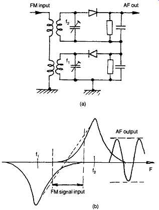
FIG. 36 The Round-Travis FM detector.
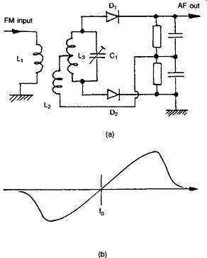
FIG. 37 The Foster-Seeley or phase detector.
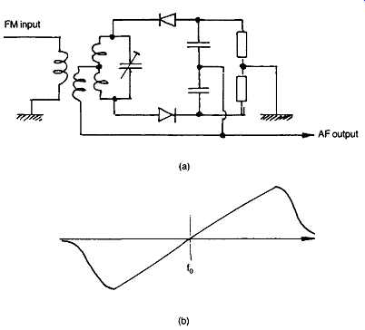
FIG. 38 The ratio detector.
The ratio detector was for many years the basic demodulator circuit for FM receivers, and offers a very good internal noise figure. This is superior to that of the contemporary IC-based phase-coincidence system, which has entirely superseded it, because of the much greater demodulation linearity offered by this latter system.
THE PHASE COINCIDENCE DEMODULATOR (PCD)
This method employs a circuit layout of the general form shown in FIG. 39, in which a group of identical bipolar transistors is interconnected so that the current from Q1, a simple constant-current source, will be routed either through Q2 or Q3, depending on the relative potential of the signal.
From Q2/Q3, the current flow will be directed either through Q4/Q7 or through Q5/Q6 and recombined at the load resistors R1 and R2.
It will be seen, from inspection, that if the transistors are well matched, the potential drop across R1 and R2 will be that due to half the output current of Q1? regardless of the relative potentials applied to Q2 or Q3 or to Q4/Q7 or Q5/Q6, so long as these potentials are not simultaneously applied.
If synchronous HF signals are applied to all four input ports (a-d), the output across R1 or R2, (output ports e and f) will only be identical if inputs c and d are at phase quadrature to those at a and b.
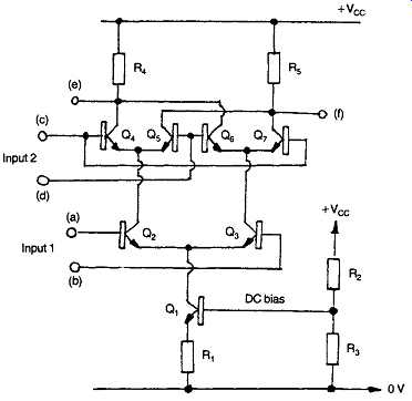
FIG. 39 Gate-coincidence transistor array.
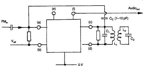
FIG. 40 Phase coincidence demodulator circuit.
Considering the circuit layout of FIG. 40, if ports b and d are taken to some appropriate DC reference potential, and an amplitude limited FM signal is applied to point a with respect to b, and some identical frequency signal, at phase quadrature at F0, is applied to c with respect to d, then there will be an output voltage at point e with respect to point f, if the input frequency is varied in respect of F0. The linearity of this VIF relationship is critically dependent on the short-term frequency/phase stability of the potential developed across the quadrature circuit (LiQ), and this depends on the Q value of the tuned circuit. The snag here is that too high a value of Q will limit the usable FM bandwidth. A normal improvement which is employed is the addition of a further tuned circuit (L2C2) to give a bandpass coupling characteristic, and further elaborations of this type are also used to improve the linearity, and lessen the harmonic distortion introduced by this type of demodulator.
The performance of this type of demodulator is improved if both the signal drive (to ports a and b) and the feed to the quadrature circuit (ports c and d) are symmetrical, and this is done in some high quality systems.
THE PHASE-LOCKED LOOP (PLL) DEMODULATOR
This employs a system of the type shown above in FIG. 26. If the voltage controlled oscillator (VCO) used in the loop has a linear input voltage versus output frequency characteristic, then when this is in frequency lock with the incoming signal the control voltage applied to the VCO will be an accurate replica of the frequency excursions of the input signal, within the limits imposed by the low-pass loop filter.
This arrangement has a great advantage over all of the preceding demodulator systems in that it’s sensitive only to the instantaneous input frequency, and not to the input signal phase. This allows a very low demodulator THD, unaffected by the phase-linearity of preceding RF and IF tuned circuits or SAW filters, and greatly reduces the cost , for a given performance standard, of the FM receiver system.
Such a circuit also has a very high figure for AM rejection and capture ratio, even when off-tune, provided that the VCO is still in lock.
Photographs of the output signal distortion, and the demodulator output voltage versus input frequency curves, taken from a frequency modulated oscillator display, are shown in Figs 41-43 , for actual commercial receivers employing ratio detector and phase coincidence demodulator systems, together with the comparable performance of an early experimental PLL receiver due to the author.
All of these units had been in use for some time, and showed the effects of the misalignment which could be expected to occur with the passage of time. When new, both the conventional FM tuners would have probably given a better performance than at the time of the subsequent t test. However, the superiority of the PLL system is evident.
Commercial manufacturers of domestic style equipment have been slow to exploit the qualities of the PLL, perhaps deterred by the unpleasant audio signal generated when the tuner is on the edge of lock. It’s not, though, a difficult matter to incorporate a muting circuit which cuts off the signal when the receiver is off tune, and an experimental system of this kind has been in use for many years.
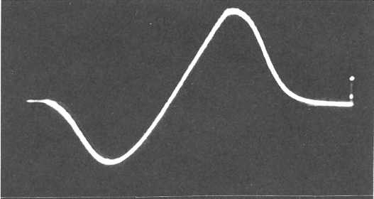
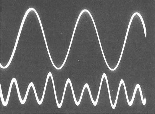
FIG. 41 Practical demodulator frequency/voltage transfer characteristics,
recovered signal, and overall receiver distortion waveform, (THD = 1.5%, mainly
third harmonic) , for ratio detector.
PULSE COUNTING SYSTEMS
In the early years of FM transmissions, when there was great interest in the exploitation of the very high quality signals then available, pulse counting systems were commonly employed as the basis for high fidelity amateur designs. Typical circuit arrangements employed were of the form shown in FIG. 44. After suitable RF amplification, the incoming signal would be mixed with a crystal controlled local oscillator signal, in a conventional superhet layout, to give a relatively low frequency IF in, say, the range 30-180 kHz, which could be amplified by a conventional broad bandwidth HF amplifier.
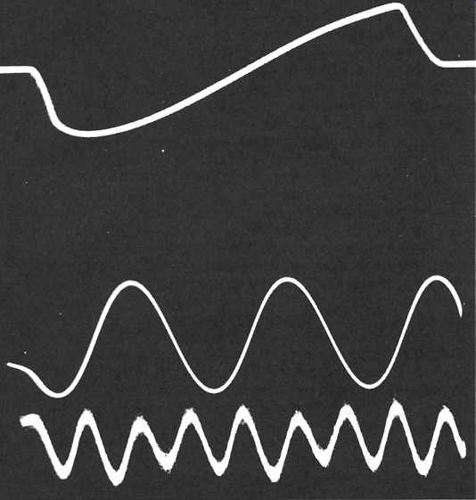
FIG. 42 Practical demodulator frequency/voltage transfer characteristics,
recovered signal, and overall receiver distortion waveform, (THD =0.6%, mainly
third harmonic) , for phase coincidence FM demodulator.
The output signal would then be analyzed by a linear rate meter circuit, to give a DC output level which was dependent on the instantaneous input signal frequency, yielding a low distortion recovered AF output.
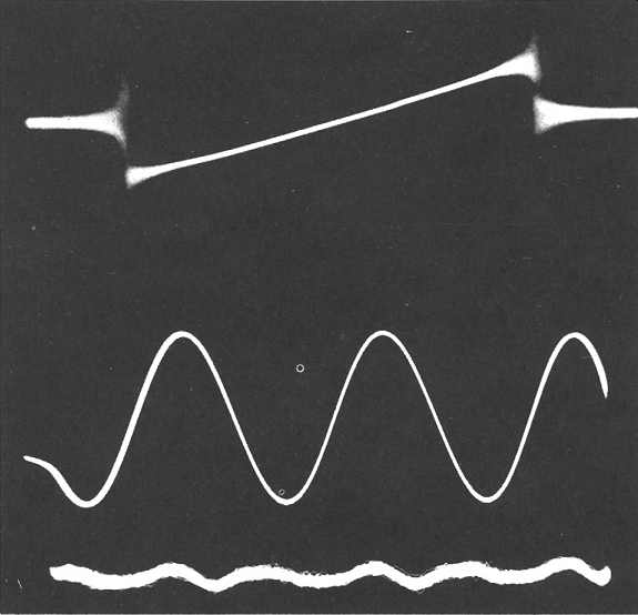
FIG. 43 Practical demodulator frequency I voltage transfer characteristics,
recovered signal, and overall receiver distortion waveform, (THD =0.15%y mainly
second harmonic) , for phase-locked loop FM demodulator.
Such systems shared the quality of the PLL demodulator that the output signal linearity was largely unaffected by the frequency/phase linearity of the preceding RF/IF circuitry. Unfortunately, they did not lend themselves well to the demodulation of stereo signals, and the method fell into disuse.
However, this technique has been resurrected by Pioneer, in its F-90/ F-99 receivers, in a manner which exploits the capabilities of modern digital ICs.
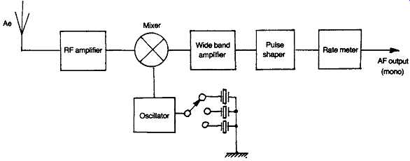
FIG. 44 Pulse counting FM tuner.
The circuit layout employed by Pioneer is shown in schematic form in FIG. 45. In this the incoming 10.7 MHz signal is frequency doubled, to double the modulation width, and mixed down to 1.26 MHz with a stable crystal controlled oscillator. After filtering, the signal is cleaned up and converted into a series of short duration pulses, having constant width and amplitude, of which the average value is the desired composite (L+R) audio signal.
A conventional PLL arrangement of the type shown in FIG. 27, is then used to reconstruct the 38 kHz sub-carrier signal, from which the LH and RH stereo outputs can be derived by adding the (L+R) + (L-R) and (L+R) + (R-L) components.
Practical FM receiver performance data:
The claimed performance from the Pioneer F-90 receiver, using this pulse counting system, is that the THD is better than 0.01% (mono) and 0.02% (stereo), with a capture ratio of better than 1 dB, and a stereo channel separation greater than 60 dB. These figures are substantially better than any obtainable with more conventional demodulator systems.
In general, the expected THD performance for a good modern FM receiver is 0.1% (mono) and 0.2-0.3% (stereo), with capture ratios in the range 1 dB (excellent) to 2.5 dB (adequate), and stereo separations in the range 30-50 dB. These figures largely depend on the type of demodulator employed, and the quality of the RF and IF circuit components and alignment.
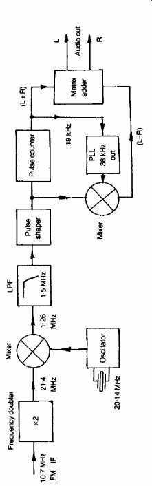
FIG. 45 The Pioneer pulse counting FM tuner system.
Typical AF bandwidths will be in the range 20-40 Hz to 14.5 kHz (-3 dB points). The LF frequency response depends on the demodulator type, with PLL and pulse counting systems allowing better LF extension.
The upper frequency limit is set by the requirements of the Zenith-GE encoding system, rather than by the receiver in use.
The ultimate signal to noise ratio of a good receiver could well be of the order of 70 dB for a mono signal, but normal reception conditions will reduce this figure somewhat, to 60 dB or so.
Input (aerial) signal strengths greatly influence the final noise figure, which worsens at low signal levels, so that input receiver sensitivities of the order of 2.5 µV and 25 µV might be expected for a 50 dB final S/N figure, on mono and stereo signals respectively, from a first quality receiver. Values of 25 µV /100 µV might be expected from less good designs.
A high (aerial) input sensitivity and a good intrinsic receiver S/N ratio is of value if the receiver is to be used with poor or badly sited aerial systems, even though the difference between receivers of widely different performance in this respect may not be noticeable with a better aerial installation.
Linearity, AM systems:
The performance of an AM radio is invariably less good than that possible from a comparable quality FM receiver. The reasons for this are partly to do with the greater difficulty in obtaining a low demodulator distortion level and a wide AF bandwidth, with a sensibly flat frequency response, coupled with good signal to noise and selectivity figures - a difficulty which is inherent in the AM system - and partly to do with the quality of the radio signal, which is often poor, both as received and as transmitted.
There are, however, differences between the various types of AM demodulator, and some of these have significant performance advantages over those normally used in practice. These are examined below.
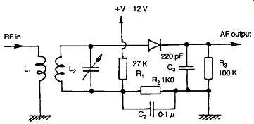
FIG. 46 Simple forward-biased diode AM detector.
THE DIODE 'ENVELOPE' DEMODULATOR
This is a direct descendant of the old crystal detector of the 'crystal and cat's-whisker' era, and is shown in FIG. 46. In this the peak voltage level occurring across the tuned circuit L C is passed through the rectifier diode, ??, and stored in the output filter circuit C3R3. Since the rectifying diode will require some forward voltage to make it conduct (about 0.15 V in the case of germanium, and 0.55 V in the case of silicon types) it’s good practice to apply a forward bias voltage, through R!R2C2, to bring the diode to the threshold of forward conduction.
Because it’s essential that the RF component is removed from the output signal, there is a minimum practical value for C3. However, since this holds the peak audio modulation voltage until it can decay through R3, a measure of waveform distortion is inevitable, especially at higher end of the audio range and at lower RF input signal frequencies.
Typical performance figures for such demodulators are 1-2% at 1 kHz.
'GRID-LEAK' DEMODULATION
This was a common system used in the days of amateur radio receivers, and shown in its thermionic valve form in FIG. 47(a). A more modern version of this arrangement, using a junction FET, is shown in FIG. 47(b). Both these circuits operate by allowing the RF signal appearing across the tuned circuit L2Q to develop a reverse bias across R1, which reduces the anode or drain currents.
The THD performance of such circuits is similar to that of the forward biased diode demodulator, but they have a lower damping effect on the preceding tuned circuits.
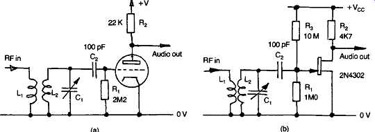
FIG. 47 Valve and FET grid-leak AM detectors.
FIG. 48 FET based anode-bend and infinite impedance detectors.
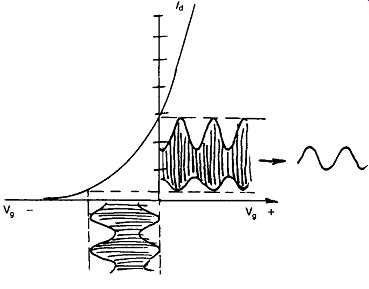
FIG. 49 Method of operation of anode-bend or infinite impedance detectors.
ANODE-BEND OR INFINITE IMPEDANCE DEMODULATOR SYSTEMS
These are shown in their junction FET versions, in Fig 48(a) and 48(b). They are similar in their action and only differ in the position of the output load. They operate by taking advantage of the inevitable curvature of the Id/Vg curve for a valve or FET to provide a distorted version of the incoming radio signal, as shown in FIG. 49, which, when averaged by some integrating circuit, gives an audio signal equivalent to the modulation.
Since the circuit distorts the incoming RF waveform, it’s unavoidable that there will be a related distortion in the recovered AF signal too.
Typical THD figures for such a demodulator system will lie in the range 0.5-1.5%, depending on signal level. Most IC AM radio systems will employ either diode envelope detectors or variations of the anode bend arrangement based on semiconductor devices.
The performance of all these systems can be improved by the addition of an unmodulated carrier, either at the same frequency, or at one substantially different from it, to improve the carrier to modulation ratio.
This is not a technique which is used for equipment destined for the domestic market, in spite of the quality improvement possible.
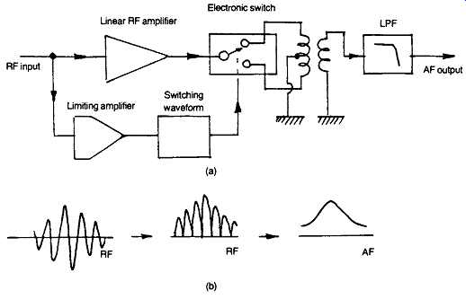
FIG. 50 Circuit layout and method of operation of Homodyne type synchronous
demodulator.
SYNCHRONOUS DEMODULATION
This method, illustrated schematically in FIG. 50(a), operates by synchronously inverting the phase of alternate halves of the RF signal, so that the two halves of the modulated carrier can be added together to give a unidirectional output. Then, when the RF component is removed by filtering, only the audio modulation waveform remains, as shown in FIG. 50(b). This technique is widely used in professional communication systems, and is capable of THD values well below 0.1%.
CIRCUIT DESIGN
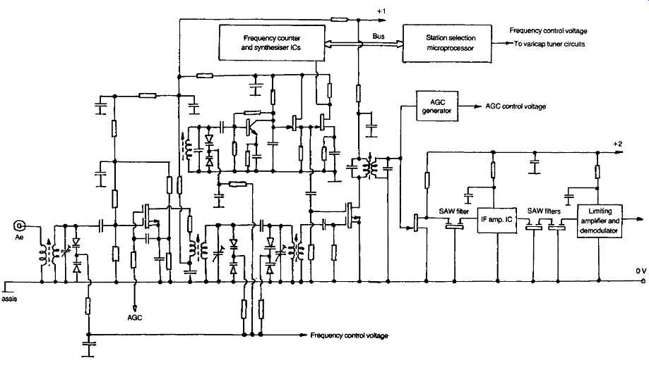
FIG. 51 Typical circuit layout of RF and IF stages of good quality contemporary
FM tuner.
Although there is a continuing interest in circuit and performance improvements made possible by new circuit and device technology, there is also a tendency towards a degree of uniformity in circuit design, as certain approaches establish themselves as the best, or the most cost-effective.
This is particularly true in the RF and IF stages of modern FM tuners, and an illustration of the type of design approach employed is given in FIG. 51. The only feature in this not covered by the previous discussion is the general use of dual (back-to-back) Varicap diodes. These are preferred to single diodes as the tuning method in high-quality systems because they avoid the distortion of the RF waveform brought about by the signal voltage modulating the diode capacitance.
Variable air-spaced ganged capacitors would be better still, but these are bulky and expensive, and don’t lend themselves to frequency synthesizer layouts.
NEW DEVELOPMENTS
In such a fast changing market it’s difficult to single out recent or projected design features for special mention, but certain trends are apparent. These mainly concern the use of microprocessor technology to memorize and store user selections of channel frequencies, as in the Quad FM4 ( FIG. 52), and the use of 'sliding stereo separation' systems to lessen the L-R channel separation, with its associated 'stereo hiss', when the incoming signal strength falls below the optimum value.
Some synthesizer tuners offer normal spin-wheel tuning, as in the Harmon-Kardon TU915, by coupling the tuning knob shaft to the synthesizer IC by the use of an optical shaft encoder.
Low-noise gallium arsenide dual-gate Mosfets have made an appearance in the Hitachi FT5500 receiver, and these devices are likely to be more widely adopted in such systems.
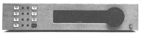
FIG. 52 The Quad FM tuner.
Clearly, commercial pressures will encourage manufacturers to develop more complex large-scale integration (LSI) integrated circuits, so that more of the receiver circuitry may be held on a single chip. This undoubtedly saves manufacturing costs, but the results are not always of benefit to the user, as evidenced by the current performance of single IC AM radio sections.
An increasing number of the better FM tuners are now offering a choice of IF bandwidths, to permit user optimization of selectivity, sensitivity or stereo separation. Variable receiver bandwidth would be a valuable feature on the MF bands, and may be offered if there is any serious attempt to improve the quality of this type of receiver.
APPENDIX 1: BROADCAST SIGNAL CHARACTERISTICS
(Data by courtesy of the BBC) Audio bandwidths MF:
• 40-5800 Hz ±3 dB, with very sharp cut off. (> 24 dB/octave beyond 6 kHz.)
• 50-5000 Hz ±1 dB. VHF:
• 30-15,000 Hz ±0.5 dB, with very sharp cut off beyond this frequency.
Distortion MF:
• < 3% THD at 75% modulation.
• < 4% THD at 100% modulation.
VHF:
• < 0.5% THD. Stereo crosstalk VHF: > 46 dB. (0.5%). Modulation depth MF: Up to 100% over the range 100-5000 Hz.
VHF: Peak deviation level corresponds to ±60.75 kHz deviation.
(The total deviation, including pilot tone, is ±75 kHz.) S/N ratio MF: > 54 dB below 100% modulation.
VHF: Up to 64 dB, using CCIR/468 weighting, with reference to peak program modulation level.
APPENDIX 2: RADIO DATA SYSTEM (RDS) (Data by courtesy of the BBC)
It was proposed to begin the introduction of this system in the Autumn of 1987, and when in use on receivers adapted to receive this signal the reception of station, program and other data is possible.
This data will include program identification, to allow the receiver to automatically locate and select the best available signal carrying the chosen program, and to display in alphanumeric form a suitable legend, and to permit display of clock time and date.
Anticipated future developments of this system include a facility for automatic selection of program type (speech/light music/serious music/ news), and for the visual display of information, such as traffic conditions, phone-in numbers, news flashes, program titles or contents, and data print out via a computer link.